 | –≠–ª–µ–∫—Ç—Ä–æ–Ω–Ω—ã–π –∫–æ–º–ø–æ–Ω–µ–Ω—Ç: FAN7685N | –°–∫–∞—á–∞—Ç—å:  PDF PDF  ZIP ZIP |
©2004 Fairchild Semiconductor Corporation
www.fairchildsemi.com
Rev. 1.1.0
Features
∑ PC Power Supply Outputs Supervisory Circuitry
∑ Few External Components
∑ Over Voltage Protection for 3.3V, 5V and 12V Outputs
∑ Under Voltage Protection for 3.3V, 5V and 12V Outputs
∑ Over Current Protection for 3.3V, 5V and 12V Outputs
∑ Dual Over Current Portection for 12V Outputs
(FAN7687)
∑ Fault Protection Output With Open Drain Output
∑ Open Drain Power Good Output
∑ 300ms Power Good Delay
∑ 38ms PSON On/Off Delay
∑ 73us Debounce
∑ 2.3ms PSON to FPO Turn Off Delay
∑ Latch Function Controlled by PSON
Typical Application
∑ PC Switching Mode Power Supply
Description
The FAN7685/FAN7686/FAN7687 is a complete output
supervisory circuitry intended for use in the secondary side
of the switched mode power supply. It provides overvoltage
protection (OVP), undervoltage protection(UVP), overcur-
rent protection (OCP), and power good signal generator to
monitor and control the outputs of the switching power sup-
ply system. Remote on/off(PSON) control and some preci-
sion protection features are also implemented.
It directly senses all the output rails for OVP, UVP, and OCP
without external divider resistors. As for output control,
power good output(PGO) and fault protection output(FPO)
are included. The FAN7685/FAN7686/FAN7687 offers a
simple and cost effective solution with minimum number of
external components and greatly reduces PCB board space
for power supply.
FAN7685/FAN7686/FAN7687
PC Power Supply Output Monitoring IC
1
14SOP
1
14DIP
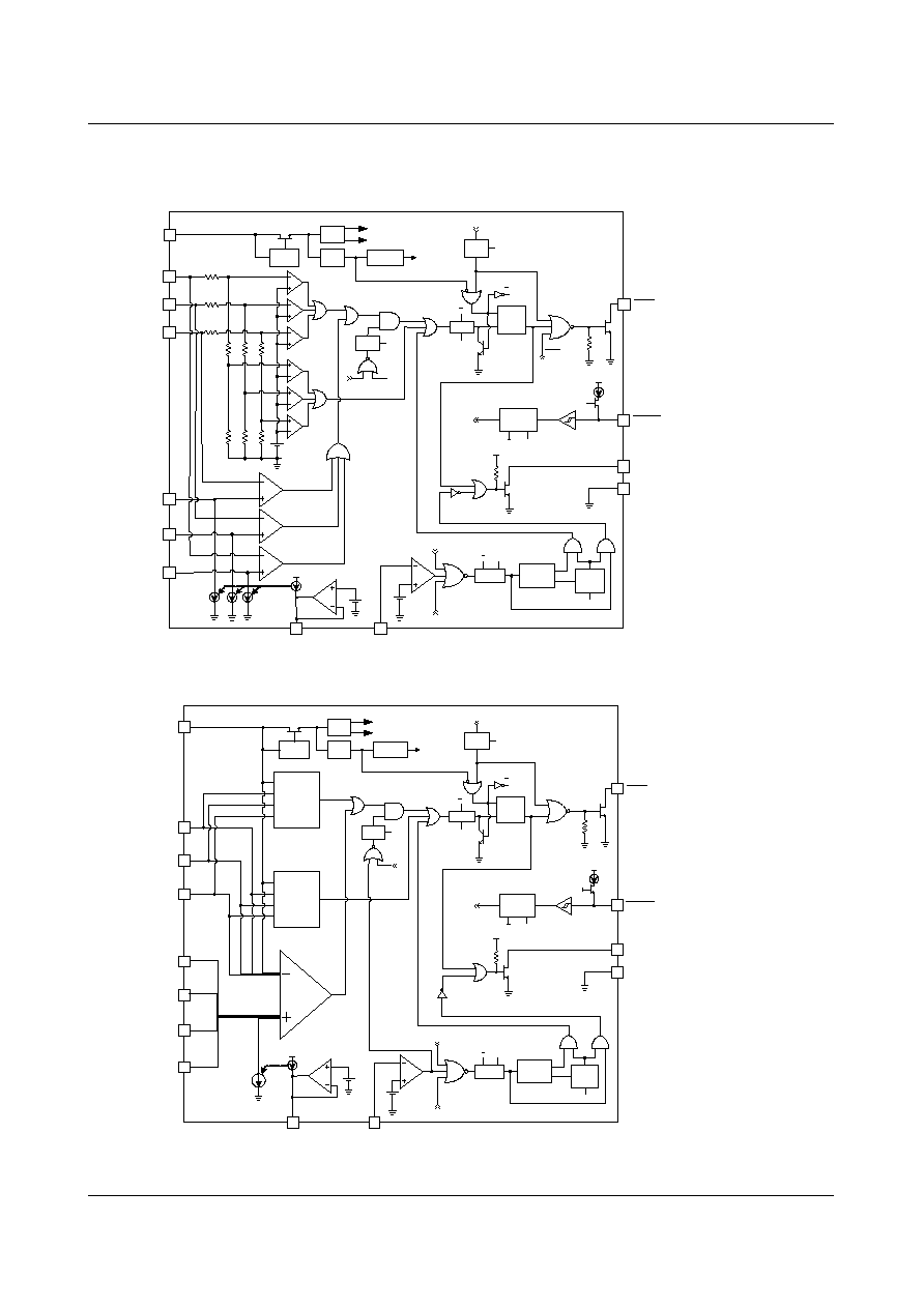
FAN7685/FAN7686/FAN7687
2
Internal Block Diagrams
UVP
OVP
Delay
75ms
S
R
Q
PGI_O
FPO
PGO
3.6V
Q
PSON
H
L
L
L
H
L
L
H
L
L
L
L
H
L
L
L
clr
R
R
Delay
2.3ms
clr
R
POR
REF.
Start-up
Vref
Reset
Vcc
Debounce
38ms
PSON
PSON
L
L
L
Vcc
3.6V
3.6V
150uA
Oscillator
CLK
CLK
CLK
CLK
CLK
R
GND
H
Vref
VS12
VS5
VS33
IS33
IS5
IS12
PGI
VCC12
1
2
14
4
3
13
10
12
11
8
ISVCC12
8*Iref
Vcc
Iref
1.2V
RI
6
FPO
Debounce
73us
UVP
L
L
H
R
CLK
Debounce
73us
H
L
PSON
Delay
300ms
H
clr
CLK
H
H
L
Short
Detector
when AC ON
L
UVP
Block
OVP
Block
OCP
COMPs
9
5
7
Power On Reset
L
(FAN7686)
FAN7687
FAN7685
UVP
OVP
Delay
75ms
Debounce
73us
S
R
Q
PGI_O
FPO
PGO
3.6V
Q
PSON
H
L
L
L
H
L
L
H
L
L
L
L
H
L
L
L
L
clr
R
R
Delay
2.3ms
clr
PWR
R
POR
REF.
Start-up
Vref
Reset
Vref
Vcc
Debounce
38ms
PSON
PSON
L
L
L
Vcc
3.6V
3.6V
150uA
Oscillator
CLK
CLK
CLK
CLK
CLK
R
GND
UVP
L
H
Vref
VS12
VS5
VS33
IS33
IS5
IS12
PGI
Vcc
Iref
1.2V
RI
Vcc
6
1
2
14
4
3
13
9
8
5
L
FPO
L
H
R
CLK
Debounce
73us
H
L
PSON
Delay
300ms
H
clr
CLK
H
H
L
Short
Detector
when AC ON
L
L
L
10
12
11
8*Iref
8*Iref
8*Iref
(7)
(8)
(9)
FAN7687A
FAN7685/FAN7686/FAN7687
3
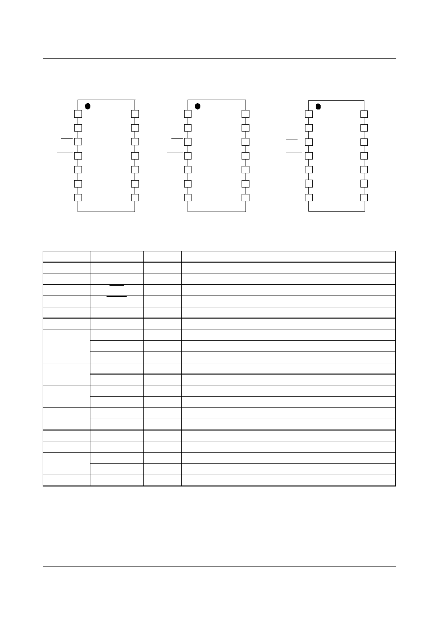
Pin Assignments
Pin Definitions
Notes :
* : FAN7686 Pin Definitions
** : FAN7687/FAN7687A Pin Definitions
Pin Number
Pin Name
I/O
Pin Function Description
1
PGI
I
Power Good Input
2
GND
-
Ground
3
FPO
O
Fault Protection Output, Open Drain Output
4
PSON
I
Remote On/Off Control Input
5
IS12
I
12V Over Current Protection
6
RI
O
Reference Current Setting Resistor
7
NC
No Connection
(FAN7685)
IS5*
I
5V Over Current Protection
(FAN7686)
ISVCC12**
I
12V-II Over Current Protection
(FAN7687)
8
IS5
I
5V Over Current Protection
(FAN7685/7)
IS33*
I
3.3V Over Current Protection
(FAN7686)
9
IS33
I
3.3V Over Current Protection
(FAN7685/7)
VS12*
I
12V Output Over/Under Voltage Protection
(FAN7686)
10
VS12
I
12V Output Over/Under Voltage Protection
(FAN7685/7)
NC*
No Connection
(FAN7686)
11
VS33
I
3.3V Output Over/Under Voltage Protection
12
VS5
I
5V Output Over/Under Voltage Protection
13
Vcc
I
Supply Voltage
(FAN7675/6)
VCC12**
I
Supply Voltage & 12V-II OV/UV Protectioin
(FAN7687)
14
PGO
O
Power Good Output, Open Drain Output
1
PSON
FPO
IS12
GND
VCC12
RI
PGO
PGI
VS12
IS33
VS5
IS5
VS33
ISVCC12
2
3
4
5
6
7
14
9
8
13
12
11
10
F
A N 76
87
FAN7687A
1
PSON
FPO
IS12
GND
V
CC
RI
PGO
PGI
VS12
IS33
VS5
IS5
VS33
NC
2
3
4
5
6
7
14
9
8
13
12
11
10
F A N 7 685
1
PSON
FPO
IS12
GND
V
CC
RI
PGO
PGI
NC
VS12
VS5
IS33
VS33
IS5
2
3
4
5
6
7
14
9
8
13
12
11
10
F A N 7 686
FAN7685/FAN7686/FAN7687
4
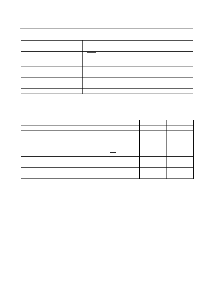
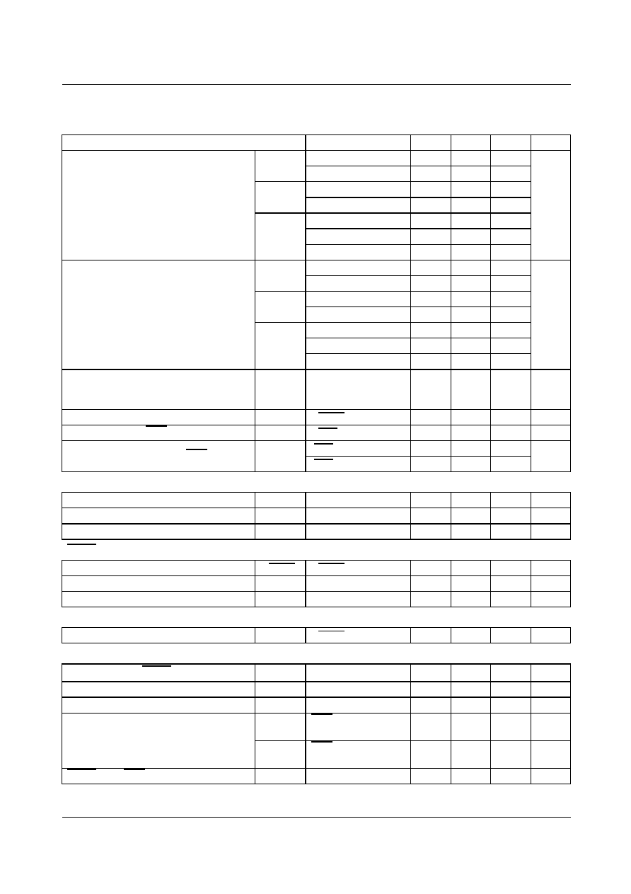
Absolute Maximum Ratings
*Note : Stresses beyond those listed under "absolute maximum ratings" may cause permanent damage to the device.
Recommended Operating Conditions
Note
1. V
CC
slew rate must be less than 14V/ms.
Parameter
Symbol
Value
Unit
Supply Voltage
V
CC
, VCC12
16
V
Input Voltage
V
PSON
, VS5, VS33, V
PGI
,
IS5, IS33
8
V
VS12, IS12, ISVCC12
16
Output Voltage
V
PGO
8
V
V
FPO
16
Operating Temperature
Topr
-40 ~ 125
∞C
Storage Temperature
Tstg
-55 ~ 150
∞C
Power Dissipation
P
D
1
W
Characteristic
Min.
Typ.
Max.
Unit
Supply Voltage
V
CC
, VCC12
4
15
V
Input Voltage
V
PSON
, VS5, VS33, V
PGI
, IS5,
IS33
-
-
7
V
VS12, IS12, ISVCC12
-
-
15
Output Voltage
V
PGO
-
-
7
V
V
FPO
-
-
15
V
Output Sink Current
I
FPO
-
-
30
mA
I
PGO
-
-
10
mA
Supply Voltage Rising Time, See Note1
tr
1
ms
Output Current for RI
I
O(RI)
12.5
-
62.5
uA
FAN7685/FAN7686/FAN7687
5
Electrical Characteristics
(V
CC
= 5V, Ta=25∞C, unless otherwise specified)
* : These parameters although guaranteed over the recommended operating conditions, are not 100% tested in production.
Over Voltage Protection, Under Voltage Protection and FPO
Parameter
Test Condition
Min.
Typ.
Max.
Unit
Over Voltage Threshold
VS33
3.9
4.1
4.3
V
FAN7687A
3.77
4.06
VS5
5.8
6.1
6.4
FAN7687A
5.71
6.16
VS12,
VCC12
13.3
13.8
14.3
FAN7687A
(VS12)
13.71
14.79
FAN7687A
(VCC12)
13.42
14.5
Under Voltage Threshold
VS33
2.55
2.69
2.83
V
FAN7687A
2.88
3.02
VS5
4.1
4.3
4.5
FAN7687A
4.37
4.58
VS12,
VCC12
8.8
9.3
9.8
FAN7687A
(VS12)
10.5
11.0
FAN7687A
(VCC12)
10.21
10.71
Ratio of Current Sense Sink Current to
Current Sense Setting Pin(RI) Source
Current
Iref
Resistor at RI=30k
,
0.1% Resistor
7.6
8
8.4
Offset Voltage of OCP Comparator
V
offset
V
PSON
=0V
-5
-
5
mV
Leakage Current(FPO)
I
LKGI
V
FPO
= 5V
-
-
5
uA
Low Level Output Voltage(FPO)
V
OLI
I
FPO
=10mA
-
-
0.3
V
I
FPO
=30mA
-
-
0.7
PGI and PGO
Input Threshold Voltage(PGI)
V
PGI
1.16
1.20
1.24
V
Leakage Current(PGO)
I
LKG2
V
PGO
= 5V
-
-
5
uA
Low Level Output Voltage(PGO)
V
OL2
I
PGO
=10mA
-
-
0.4
V
PSON Control
Input Pull-up Current
I
PSON
V
PSON
= 0V
-
150
-
uA
High-Level Input Voltage
V
IHPS
2.4
-
-
V
Low-Level Input Voltage
V
ILPS
-
-
1.2
V
Total Device
Supply Current
I
CC
V
PSON
= 5V
-
-
1
mA
Switching Characteristics
Debounce Time(PSON)
t
b1
25
38
51
ms
Noise Debounce Time
t
b2*
50
73
100
us
PGO Delay Time(PGI to PGO)
t
d1
200
300
410
ms
Internal UVP Delay Time
t
d2
FPO goes low and
every time PGI > 1.2
51
75
102
ms
t
d4*
FPO goes low and
everytime PGI<1.2
200
300
410
ms
PSON off to FPO Delay Time
t
d3
t
b1
+1.6 t
b1
+2.3 t
b1
+3.2
ms

FAN7685/FAN7686/FAN7687
6
Timing Chart
1) AC Input ON/OFF - Normal State
2) PSON ON/OFF - Normal State
V
CC
PGI
FPO
PSON
OUT
PGO
POR
t
b1
AC Input
Enable
AC Input
Disable
UVP
Threshold
t
b2
+t
d1
PGI
FPO
PSON
OUT
PGO
t
d3
t
b1
+t
b2
t
b1
UVP
Threshold
t
b2
+t
d1
FAN7685/FAN7686/FAN7687
7
3) Under Voltage at Normal State
4) Under Voltage at AC Input ON
PGI
FPO
PSON
OUT
PGO
t
b2
t
b1
UVP
Threshold
t
b2
+t
d1
UVP
Threshold
Latch
V
CC
PGI
FPO
PSON
OUT
PGO
POR
t
b1
AC Input
Enable
PGI
Threshold
t
b2
+t
d2
UVP
Threshold
t
b2
+t
d1
Latch

FAN7685/FAN7686/FAN7687
8
5) Under Voltage at PSON ON/OFF
6) Over Voltage at PSON ON/OFF
PGI
FPO
PSON
OUT
PGO
t
d3
t
b1
+t
b2
UVP
Threshold
t
b2
+t
d1
t
b1
PGI
Threshold
t
b2
+t
d2
Latch
PGI
FPO
PSON
OUT
PGO
t
b2
t
b1
UVP
Threshold
t
b2
+t
d1
OVP
Threshold
Latch

FAN7685/FAN7686/FAN7687
9
Typical Application Circuits
PWM
12V Output
VS12
VS5
VS33
5Vsb
VS5
VS33
VS12
PGO
5V Output
3.3V Output
5Vsb
PSON
5V Coil
3.3V Coil
R
S_12V
R
S_5V
R
S_3.3V
IS5
R
IS5
IS33
R
IS33
IS12
R
IS12
PSON
FPO
IS12
GND
V
CC
RI
PGO
PGI
VS12
IS33
VS5
IS5
VS33
NC
1
2
3
4
5
6
7
14
13
12
11
10
9
8
F A
N 76
85
PWM
12V-I Output
VS12
VS5
VS33
5Vsb
VS5
VS33
VS12
PGO
5V Output
3.3V Output
12V-II Output
5Vsb
PSON
5V Coil
3.3V Coil
12V_II Coil
R
S_12V-I
R
S_5V
R
S_3.3V
R
S_12V-II
IS5
R
IS5
IS33
R
IS33
ISVCC12
R
ISVCC12
IS12
R
IS12
IS33
IS5
IS12
ISVCC12
PSON
FPO
IS12
GND
VCC12
RI
PGO
PGI
VS12
IS33
VS5
IS5
VS33
ISVCC12
1
2
3
4
5
6
7
14
13
12
11
10
9
8
F A N
76
87
FAN7685 Application Circuit
FAN7687 Application Circuit
FAN7685/FAN7686/FAN7687
10
Application Information
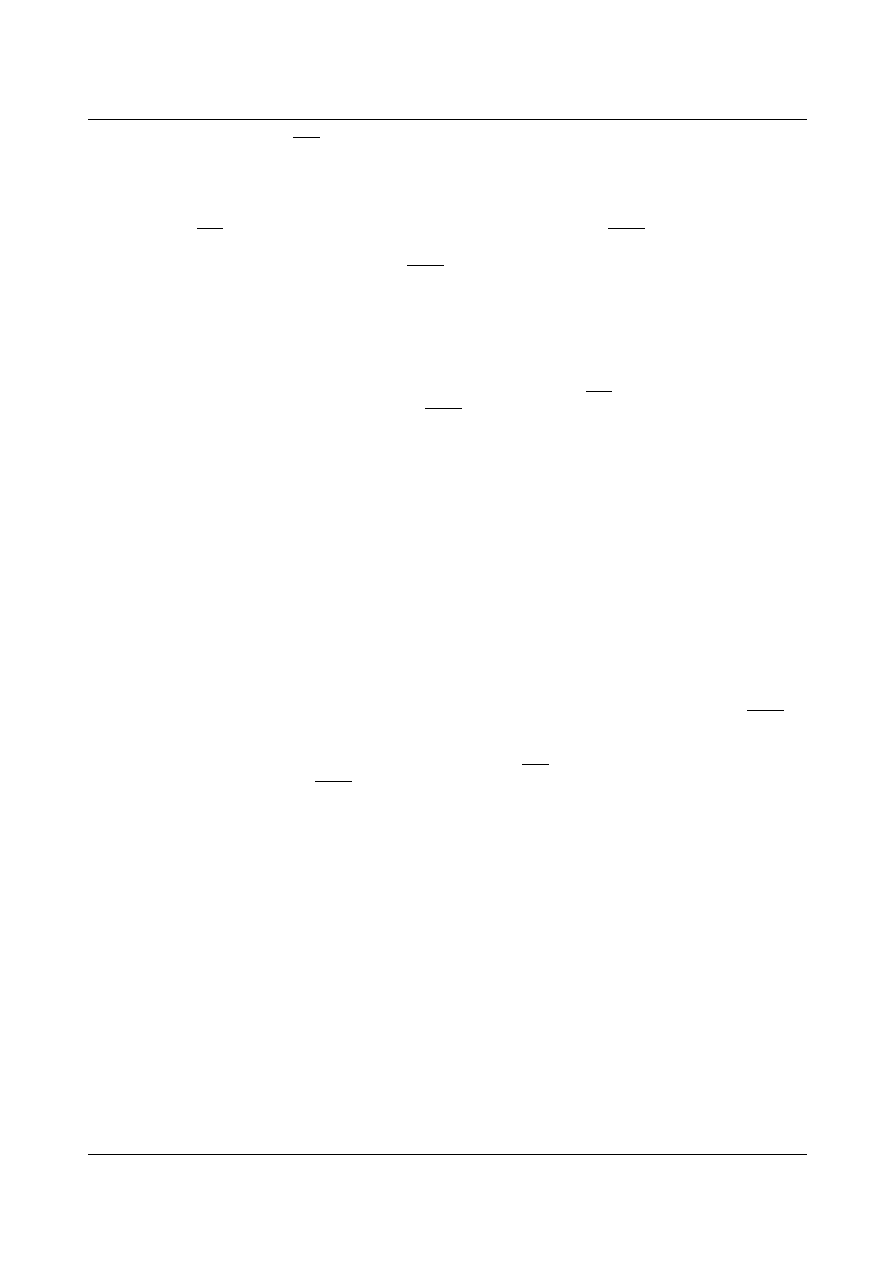
Power Good(PGO) and Power Good Delay
A PC power supply is commonly designed to provide the motherboard with a power good signal, which is defined by the com-
puter manufacturers. If the +3.3V, +5V, and +12V outputs are above the undervoltage threshold limit, the PC power supply
makes the power good signal high. At this time the power supply should be able to provide enough power to assure continuous
operation within the specification. Conversely, when one of the +3.3V, +5V, or +12V outputs falls below the undervoltage
threshold or rises above the overvoltage threshold, or when main power has been turned off for a sufficiently long time so that
power supply operation is no longer assured, a PGO signal will be a low state.
The AC input, power good(PGO), remote on/off(PSON), and +3.3V/+5V/+12V supply rails are shown in the below figure.
Although there is no requirement to meet specific timing parameters, the following signal timings are recommended :
-T1(Power On Time) : T1 <
500ms
-T2(Rise Time) : 0.1ms
T2 20ms
-T3(PGO Delay) : 100ms < T3 <500ms
-T4(PGO Delay Risetime) : T4
10ms
-T5(AC Loss to PGO Hold-Up Time) : T5
16ms
-T6(Power Down Warning) : T6
1ms
Furthermore, motherboards should be designed to comply with the above recommended timing range. If timings other than
these are implemented or required, that information should be clearly specified.
The FAN7685/FAN7686/FAN7687 provide a power good(PGO) signal for the +3.3V, +5V and +12V supply voltage rails and
a separate power good input(PGI). An internal delay circuit is used to generate a 300ms power good delay.
If voltages at PGI(+1.2V), VS33(+3.3V), VS5(+5V), and VS12(+12V) rise above the undervoltage threshold, the open drain
power good output(PGO) will go high after a delay of 300ms. When the PGI voltage or any of +3.3V, +5V, and +12V rails
drops below the undervoltage threshold, the PGO signal will be disabled immediately.
Power Supply Remote On/Off(PSON) and Fault Protection Output(FPO)
Since the latest personal computer generation focuses on easy turn on and power saving functions, a PC power supply will
require two characteristics. One is a dc power supply remote on/off function; the other is standby power to achieve very low
power consumption of the PC power supply. Thus, the main power needs to be shut down.
The power supply remote on/off(PSON) is an active-low signal that turns on all of the main power rails including the +3.3V,
+5V, and +12V power rails. When this signal is held high by the PC motherboard or left open circuited, the signal of the fault
protect output(FPO) also goes high. Thus, the main power rails can not deliver current and are held at 0V.
When the FPO signal is held high due to a fault condition, the fault status will be latched and the outputs of the main power
rails can not deliver current and are held at 0V. Toggling the PSON input signal from low to high will reset the fault protection
latch. During this fault condition only the standby power is not affected.
When the PSON input signal goes from high to low or low to high, the 38ms debounce block will be active to avoid that a
glitch on the PSON input may disable/enable the FPO output. When the PSON is set low, the undervoltage function is disabled
for 75ms to avoid turn-on failure. At turn-off, there is an additional delay of 2.3ms from PSON to FPO.
Power should be delivered to the rails only when the PSON signal is held at ground potential, thus the FPO becomes a low
T1
T5
T6
T4
T3
T2
PGO
+12VDC
+5VDC
+3.3VDC
PSON
VAC
95%
10%
FAN7685/FAN7686/FAN7687
11
state after a debounce of 38ms. The FPO pin can be connected to +5V(or up to +15V) through a pull-up resistor.
Under Voltage Protection
The FAN7685/FAN7686/FAN7687 provide undervoltage protection(UVP) for the +3.3V, +5V, and +12V power rails. When
an undervoltage condition appears at one of the VS33(+3.3V), VS5(+5V), or VS12(+12V) input pins for more than 73us, the
PGO goes low and FPO output goes high. Also, this fault condition will be latched until the PSON is toggled from low to high
or the Vcc falls below a minimum operating voltage.
When the power supply is turned on by the AC input or PSON, an internal UVP delay time is 75ms. But at normal state an
UVP delay time is only a 73us debounce time. The need for undervoltage protection is often overlooked in off-line switching
power supply system design. But it is very important in battery powered or hand-held equipment since the TTL or CMOS
logic often malfunctions under UVP condition.
Over Voltage Protection(OVP)
The overvoltage protection(OVP) of the FAN7685/FAN7686/FAN7687 monitor +3.3V, +5V, and +12V. When an overvoltage
condition appears at one of the +3.3V, +5V, or +12V input pins for more than 73us, the FPO output goes high and the PGO
goes low. Also, this fault condition will be latched until the PSON is toggled from low to high or Vcc drops below a minimum
operating voltage. During overvoltage condition, most power supplies have the potential to deliver higher output voltages than
those normally specified or required. In unprotected equipment, it is possible for output voltages to be high enough to cause
internal or external damage to the system. To protect the system under these abnormal conditions, it is common practice to pro-
vide overvoltage protection within the power supply.
Because TTL and CMOS circuits are very vulnerable to overvoltage, it is becoming industry standard to provide overvoltage
protection on all +3.3V, +5V, and +12V outputs. Therefore, not only the +3.3V and +5V rails for the logic circuits on the moth-
erboard need to be protected, but also the +12V peripheral devices such as the hard disk, flopply disk, and CD-ROM players
etc., need to be protected.
Over Current Protection
In bridge or forward type, off-line switching power supplies, usually designed from medium to large power, the overload pro-
tection design needs to be very precise. Most of these types of power supplies are sensing the output current for an overload
condition. The trigger point needs to be set higher than the maximum load in order to prevent false turn-on.
During safety testing the power supply might have tied the output voltage direct to ground. If this happens during the nomal
operating, this is called a short-circuit or over current condition. When it happens before the power supply turns on, this is
called a short-circuit power supply turn-on. It can happen during the design period, in the production line, at quality control
inspection or at the end user. The FAN7685/FAN7686/FAN7687 provide an UVP and OCP with a 75ms delay after PSON is
set low.
The FAN7685/FAN7686/FAN7687 provide overcurrent protection(OCP) for the 3.3V, 5V, and 12V rails. When an overcurrent
condition appears at the OCP comparator input pins for more than 73us, the FPO output goes high and PGO goes low. Also,
this fault condition will be latched until PSON is toggled from low to high or Vcc is removed.
The resistor connected between the RI pin and the GND pin will introduce an accurate I
O(RI)
for the OCP function. Of course,
a more accurate resistor tolerance will be better. The formula for choosing the RI resistor is V
RI
/I
O(RI)
. The I
O(RI)
range is
from 12.5uA to 62.5uA. Four OCP comparators and the I
O(RI)
section are supplied by VS12. Current drawn from the VS12pin
is less than 1mA.
Following is an example on calculating OCP for the 12V rail :
RI
V
RI
I
O RI
( )
--------------
1.2V
20uA
--------------
60k
=
=
=
I
O RI
(
)
K R
IS12
(
)
R
sense
(
)
=
◊
◊
I
OCP Trip
≠
(
)
◊
I
OCP Trip
≠
(
)
20u 8 560
◊
0.01
(
)
/
◊
=
9.2A
=

FAN7685/FAN7686/FAN7687
12
Mechanical Dimensions
Package
Dimensions in millimeters/inches
14-DIP

FAN7685/FAN7686/FAN7687
13
Mechanical Dimensions
Package
Dimensions in millimeters/inches
14-SOP
FAN7685/FAN7686/FAN7687
3/9/04 0.0m 001
Stock#DSxxxxxxxx
2004 Fairchild Semiconductor Corporation
LIFE SUPPORT POLICY
FAIRCHILD'S PRODUCTS ARE NOT AUTHORIZED FOR USE AS CRITICAL COMPONENTS IN LIFE SUPPORT DEVICES
OR SYSTEMS WITHOUT THE EXPRESS WRITTEN APPROVAL OF THE PRESIDENT OF FAIRCHILD SEMICONDUCTOR
CORPORATION. As used herein:
1. Life support devices or systems are devices or systems
which, (a) are intended for surgical implant into the body,
or (b) support or sustain life, and (c) whose failure to
perform when properly used in accordance with
instructions for use provided in the labeling, can be
reasonably expected to result in a significant injury of the
user.
2. A critical component in any component of a life support
device or system whose failure to perform can be
reasonably expected to cause the failure of the life support
device or system, or to affect its safety or effectiveness.
www.fairchildsemi.com
DISCLAIMER
FAIRCHILD SEMICONDUCTOR RESERVES THE RIGHT TO MAKE CHANGES WITHOUT FURTHER NOTICE TO ANY
PRODUCTS HEREIN TO IMPROVE RELIABILITY, FUNCTION OR DESIGN. FAIRCHILD DOES NOT ASSUME ANY
LIABILITY ARISING OUT OF THE APPLICATION OR USE OF ANY PRODUCT OR CIRCUIT DESCRIBED HEREIN; NEITHER
DOES IT CONVEY ANY LICENSE UNDER ITS PATENT RIGHTS, NOR THE RIGHTS OF OTHERS.
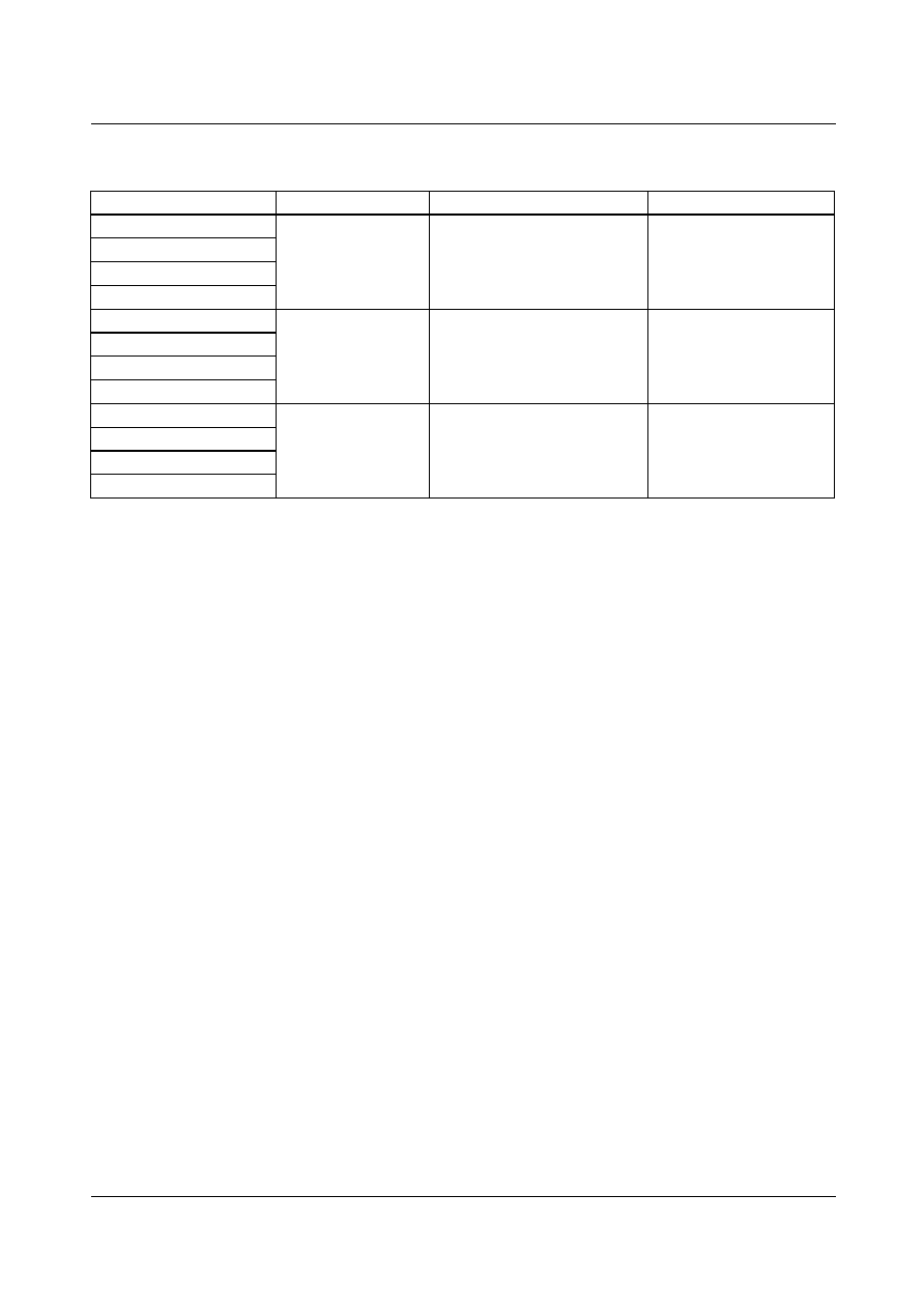
Ordering Information
Product Number
Package
Operating Temperature
Packing
FAN7685N
14DIP
-40 ~ 125
∞C
Tube
FAN7686N
FAN7687N
FAN7687AN
FAN7685M
14SOP
-40 ~ 125
∞C
Tube
FAN7686M
FAN7687M
FAN7687AM
FAN7685MX
14SOP
-40 ~ 125
∞C
Tape & Reel
FAN7686MX
FAN7687MX
FAN7687AMX