©2000 Fairchild Semiconductor International
www.fairchildsemi.com
Rev. .1.0.1
February. 2000.
1
Features
∑ Built in 4-CH balanced transformerless(BTL) driver
∑ Output gain adjustable
∑ Built in normal OP-amp
∑ Built in mute function
∑ Built in level shift circuit
∑ Built in thermal shutdown function
∑ Operating range 4.5~13.2V
Description
The FAN8000D is a monolithic integrated circuit, suitable
for 4-CH motor driver which drives tracking actuator, focus
actuator, sled motor and tray motor of CD/CD-ROM/DVD
system.
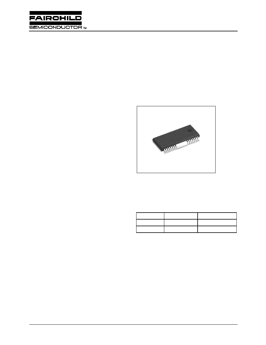
28-SSOPH-375
FAN8000D (KA9268D)
4-CH Motor Driver
Target Application
∑ Compact disk player
∑ Video compact disk player
∑ Digital Video Disk Player
∑ Car compact disk player
Ordering Information
Device
Package
Operating Temp.
FAN8000D
28-SSOPH-375
-
40
∞
C ~ +85
∞
C
FAN8000DTF 28-SSOPH-375
-
40
∞
C ~ +85
∞
C
FAN8000D (KA9268D)
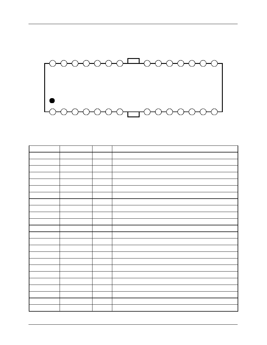
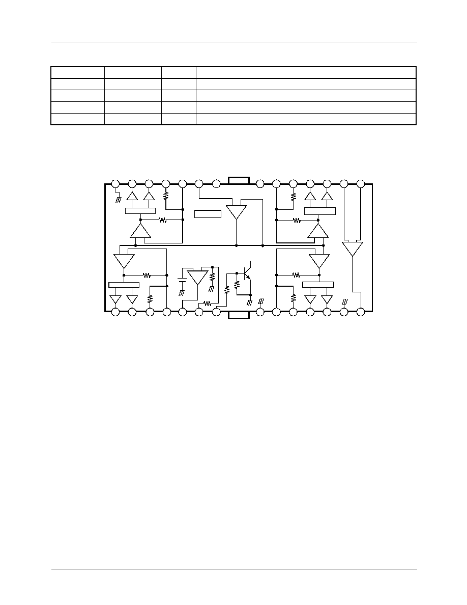
5
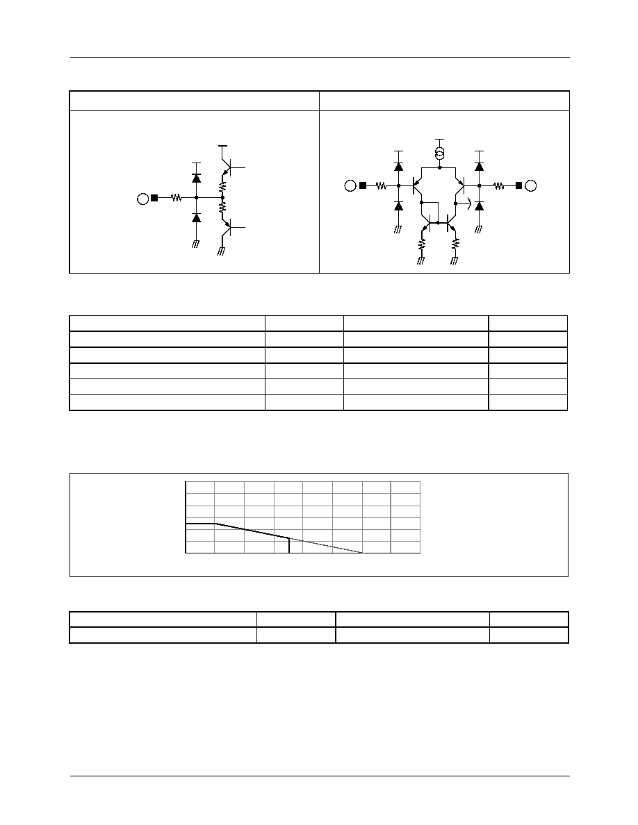
Equivalent Circuits (Continued)
Absolute Maximum Ratings ( Ta=25
∞
∞
∞
∞
C)
Notes:
1. When mounted on 76.2mm
◊
114mm
◊
1.57mm PCB (Phenolic resin material).
2. Power dissipation reduces 13.6mW /
∞
C for using above Ta=25
∞
C
3. Do not exceed Pd and SOA (Safe Operating Area).
Recommended Operating Condition ( Ta=25
∞
∞
∞
∞
C)
Op amp output
Op amp input
Parameter
Symbol
Value
Unit
Supply voltage
V
CC
18
V
Power dissipation
P
D
1.7
note
W
Operating temperature
T
OPR
-
40 ~ +85
∞
C
Storage temperature
T
STG
-
55 ~ +150
∞
C
Maximum output current
I
OMAX
1
A
Parameter
Symbol
Value
Unit
Operating supply voltage
V
CC
4.5 ~ 13.2
V
14
50
50
VCC
VCC
50
15
VCC
50
VCC
VCC
16
50
4.8k
4.8k
3,000
2,000
1,000
0
0
25
50
75
100
125
150
175
Pd (mW)
Ambient temperature, Ta [
∞
C]