©2001 Fairchild Semiconductor Corporation
www.fairchildsemi.com
Rev. 1.0.2
Features
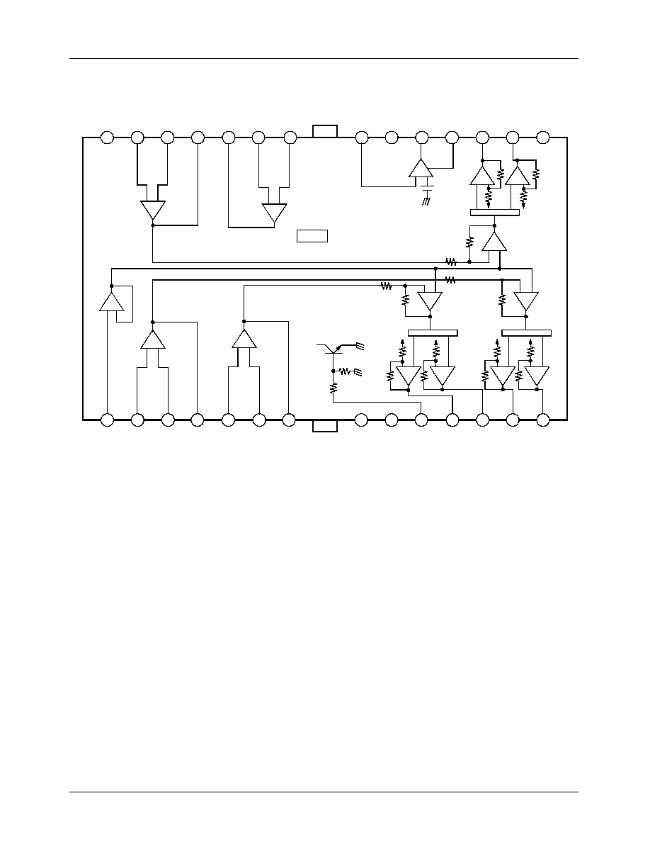
∑ 3-Channel BTL (Balanced transformer-less) driver
∑ Built-in variable regulator with reset (Series-REG)
∑ Built-in thermal shutdown circuit
∑ Built-in power save circuit
∑ Built-in general OP-amp
∑ Operating supply voltage: 4.5V ~ 5.5V
∑ Corresponds to 3.3V or 5V DSP
Description
The FAN8005D2 is a monolithic integrated circuit, suitable
for a 3-ch motor driver which drives focus actuator, tracking
actuator, and sled motor of a CD-media system.
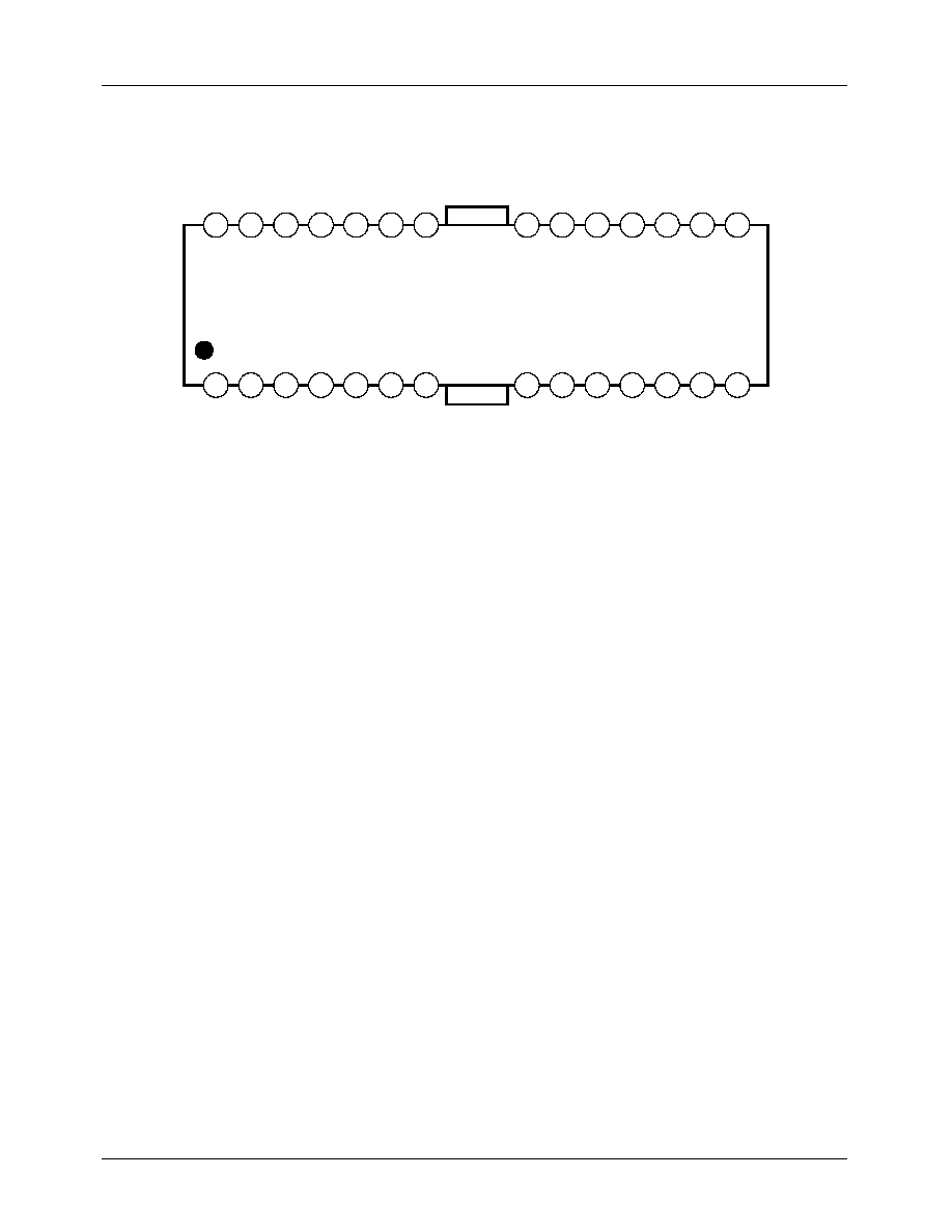
28-SSOPH-300
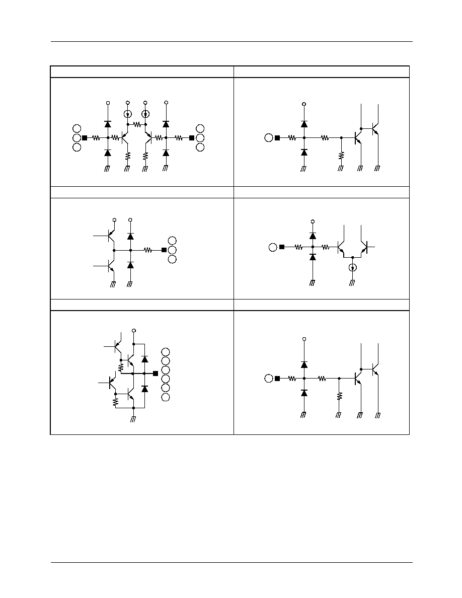
FAN8005D2
3-CH Motor Driver
Typical Applications
∑ Compact disk player
∑ Digital video disk player
∑ Compact disk ROM
Ordering Information
Device
Package
Operating Temp.
FAN8005D2
28-SSOPH-300
-
35
∞
C ~ +85
∞
C
FAN8005D2TF 28-SSOPH-300
-
35
∞
C ~ +85
∞
C