©2002 Fairchild Semiconductor Corporation
www.fairchildsemi.com
Rev. 1.0.1
Features
∑ 2-Channel BTL driver with current feedback
∑ 2-Channel BTL DC motor driver
∑ Built-in thermal shutdown circuit
∑ Built-in mute circuit
∑ Operating supply voltage: 4.5~13.2V
Description
The FAN8024BD is a monolithic IC, suitable for 2-ch BTL
DC motor drivers and 2-ch motor drivers with current
feedback which drive the focus and tracking actuators of a
CD- media system.
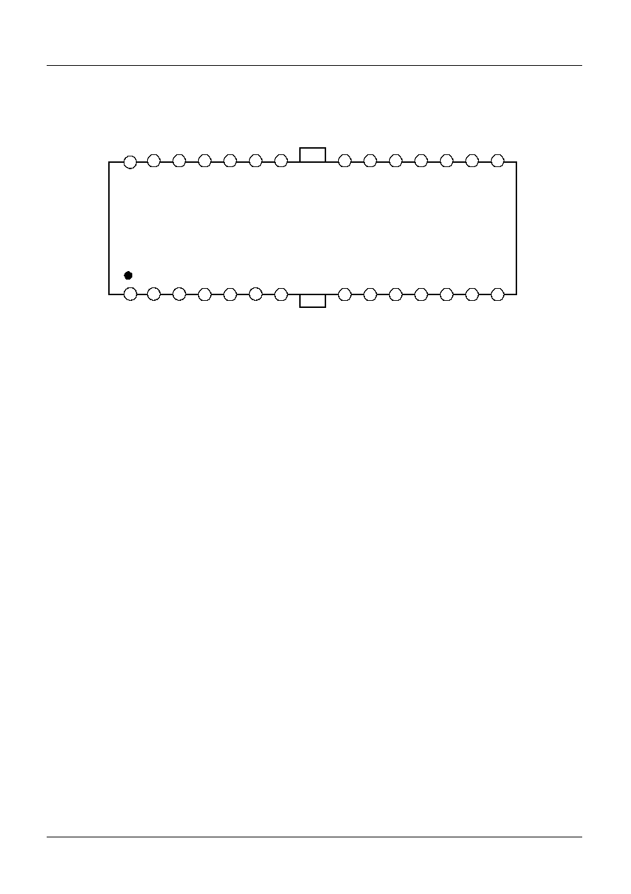
28-SSOPH-375
Typical Applications
∑ Compact disk ROM (CD-ROM)
∑ Compact disk RW (CD-RW)
∑ Digital video disk ROM (DVD-ROM)
∑ Digital video disk RAM (DVD-RAM)
∑ Digital video disk player (DVDP)
∑ Other compact disk media
Ordering Information
Device
Package
Operating Temp.
FAN8024BD
28-SSOPH-375
-25
∞
C ~ 85
∞
C
FAN8024BDTF 28-SSOPH-375
-25
∞
C ~ 85
∞
C
FAN8024BD
4-Channel Motor Driver