©2003 Fairchild Semiconductor Corporation
www.fairchildsemi.com
Rev. 1.0.0
Features
∑ 2-Channel BTL drivers with current feedback
∑ 2-Channel BTL DC motor drivers
∑ 1-Channel Logic input loading driver
∑ Built-in thermal shutdown circuit
∑ Built-in mute circuit
∑ Operating supply voltage: 4.5~13.2V
Description
The FAN8025G3 is a monolithic IC, suitable for 2-ch BTL
DC motor drivers, 2-ch motor drivers with current feedback
which drive the focus and the tracking actuator and 1-ch
logic input loading driver.
28-SSOPH-375SG2
Typical Applications
∑ Compact disk ROM (CD-ROM)
∑ Digital video disk player (DVDP)
∑ Video compact disk player(VCDP)
∑ Other compact disk media
Ordering Information
X:Tape & Reel type
Device
Package
Operating Temp.
FAN8025G3
28-SSOPH-
375SG2
-35
∞
C ~ 85
∞
C
FAN8025G3X
28-SSOPH-
375SG2
-35
∞
C ~ 85
∞
C
FAN8025G3
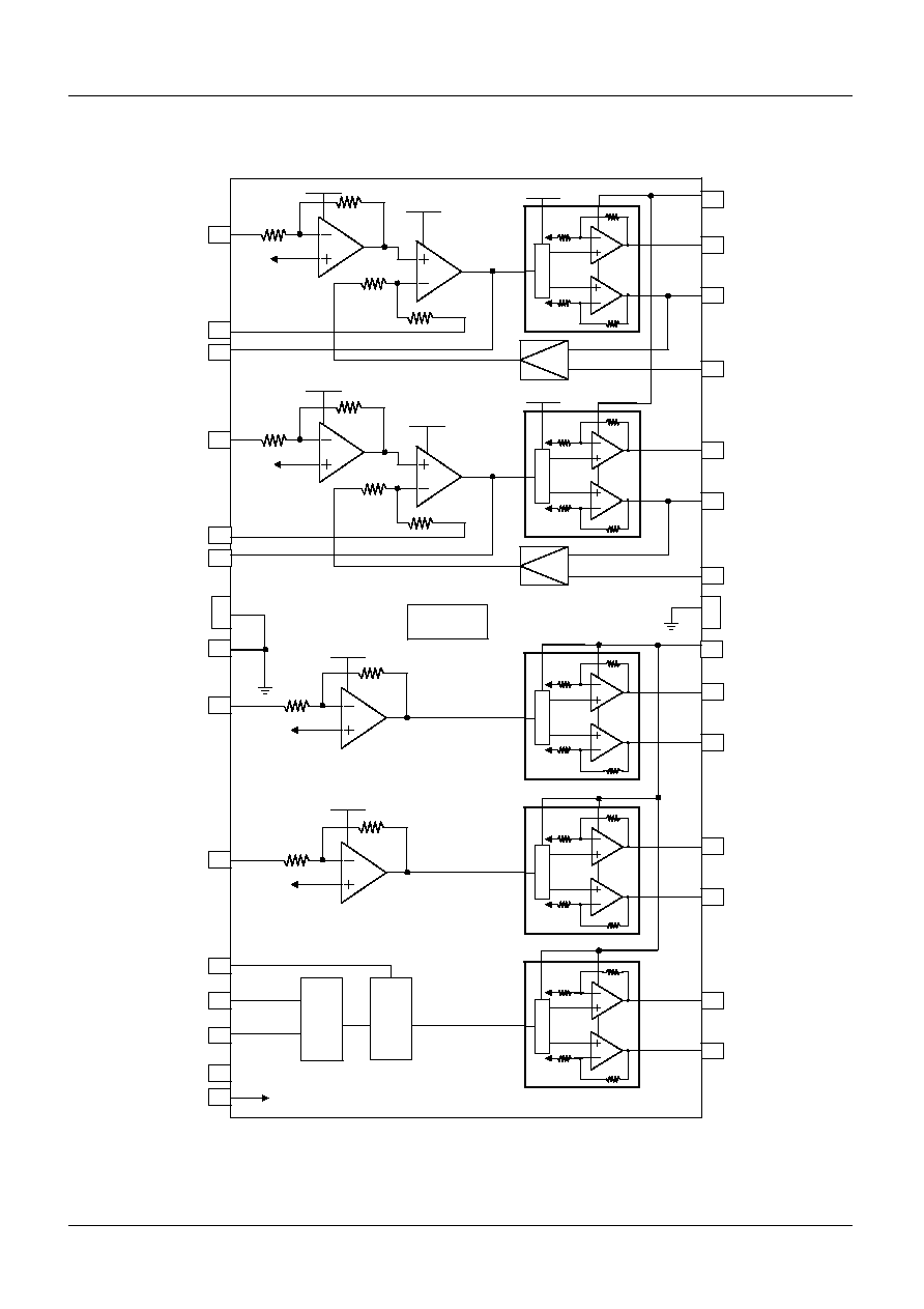
5-Channel Motor Driver

FAN8025G3
3
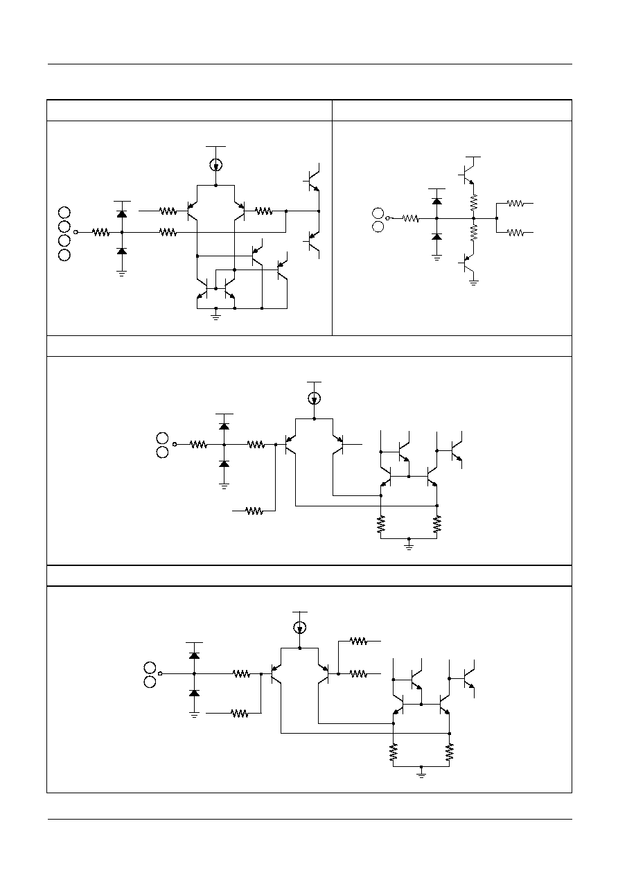
Pin Definitions
Pin Number
Pin Name
I/O
Pin Function Description
1
IN5
A
CH5 input
2
CAP5.1
A
Connection with capacitor
3
CAP5.2
A
for CH5
4
FB5
A
Feedback for CH5
5
FB4
A
Feedback for CH4
6
CAP4.1
A
Connection with capacitor
7
CAP4.2
A
for CH4
8
SGND
P
Signal ground
9
IN4
A
CH4 input
10
CTL
A
CH1 speed control input
11
FWD
I
CH1 forward input
12
REV
I
CH1 reverse input
13
DO1+
O
Drive1 Output (
+
)
14
DO1
-
O
Drive1 Output (
-
)
15
DO2
-
O
Drive2 Output (
-
)
16
DO2
+
O
Drive2 Output (
+
)
17
DO3
-
O
Drive3 Output (
-
)
18
DO3+
O
Drive3 Output (
+
)
19
VCC1
P
Power for channel 1,2 and 3
20
IN3
A
CH3 input
21
IN2
A
CH2 input
22
REF
A
Bias voltage input
23
MUTE
I
CH2,3,4 and 5 mute signal input
24
VCC2
P
Power for channel 4and 5
25
DO4+
O
Drive4 Output (+)
26
DO4
-
O
Drive4 Output (
-
)
27
DO5+
O
Drive5 Output (
+
)
28
DO5
-
O
Drive5 Output (
-
)