
©2004 Fairchild Semiconductor Corporation
www.fairchildsemi.com
Rev. 1.0.0
Features
∑ 5-CH Balanced transformerless (BTL) driver
∑ Operating supply voltage : 4.5 V ~ 13.2V
∑ Built-in thermal shut down circuit (TSD)
∑ Built-in channel mute circuit
∑ Built-in 1-OP AMP
Description
The FAN8026G3 is a monolithic integrated circuit suitable
for a 5-CH motor driver which drives a tracking actuator, a
focus actuator, a sled motor, a spindle motor, and a tray
motor of the CDP/CAR-CD/DVDP systems.
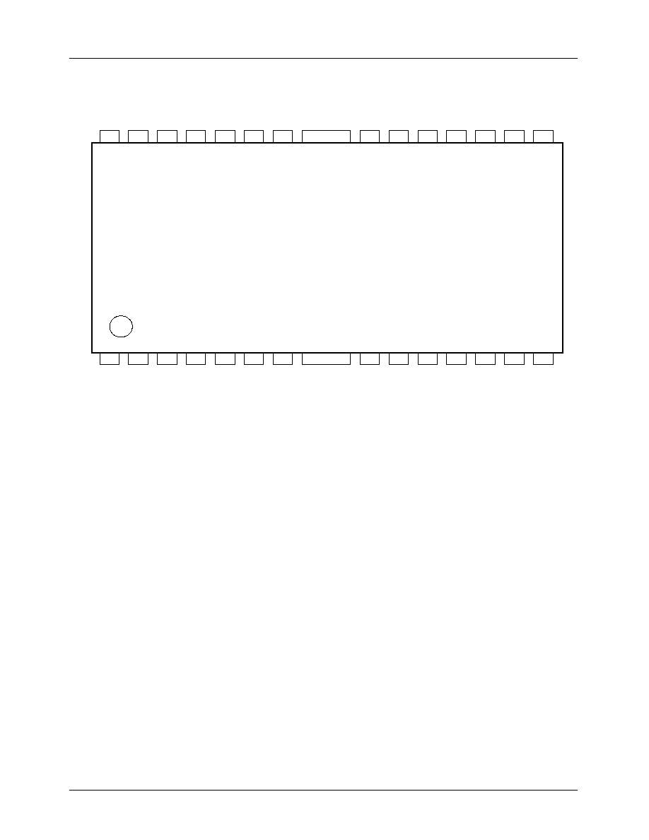
28-SSOPH-375SG3
FAN8026G3
5-CH Motor Driver
Typical application
∑ Compact disk player
∑ Video compact disk player
∑ Car compact disk player
∑ Digital video disk player
Ordering information
Notes:
1. X : Tape&Reel
2. NL : Lead free
Device
Package
Operating
temp
FAN8026G3
28-SSOPH-375-SG2 -35
∞C ~ +85∞C
FAN8026G3X
note1
28-SSOPH-375-SG2 -35
∞C ~ +85∞C
FAN8026G3_NL
note2
28-SSOPH-375-SG2 -35
∞C ~ +85∞C
FAN8026G3X_NL
28-SSOPH-375-SG2 -35
∞C ~ +85∞C
FAN8026G3
2
Pin Assignments
OPIN+
OPIN-
OPOUT
IN5
OUT5
IN4
OUT4
GND
IN2
OUT2
IN1
VM1
DO3+
DO3-
DO2-
DO2+
DO1-
DO1+
SVCC
OUT3
IN3
MUTE
REF
VM2
DO4+
DO4-
DO5+
DO5-
FAN8026G3
1
2
3
4
5
6
7
8
9
10
11
12
13
14
FIN
28
27
26
25
24
23
22
21
20
19
18
17
16
15
FIN

FAN8026G3
3
Pin Definitions
Pin Number
Pin Name
I/O
Pin Function Description
1
OPIN+
I
OP-AMP Input(+)
2
OPIN-
I
OP-AMP Input(-)
3
OPOUT
O
OP-AMP Output
4
IN5
I
CH5 Op-amp Input(-)
5
OUT5
O
CH5 Op-amp Output
6
IN4
I
CH4 Op-amp Input(-)
7
OUT4
O
CH4 Op-amp Output
8
GND
-
Ground
9
IN2
I
CH2 Op-amp Input(-)
10
OUT2
O
CH2 Op-amp Output
11
IN1
I
CH1 Input
12
VM1
-
Power Supply Voltage(For CH2,CH3)
13
DO3+
O
CH3 Drive Output(+)
14
DO3-
O
CH3 Drive Output(-)
15
DO2-
O
CH2 Drive Output(-)
16
DO2+
O
CH2 Drive Output(+)
17
DO1-
O
CH1 Drive Output(-)
18
DO1+
O
CH1 Drive Output(+)
19
SVCC
-
Power Supply Voltage(For Signal,CH1)
20
OUT3
O
CH3 Op-amp Output
21
IN3
I
CH3 Op-amp Input(-)
22
REF
I
CH1,2,3,4,5 Input Reference
23
MUTE
I
MUTE(CH2,3,4,5)
24
VM2
-
Power Supply Voltage(For CH4,CH5,Normal Op-amp)
25
DO4+
O
CH4 Drive Output(+)
26
DO4-
O
CH4 Drive Output(-)
27
DO5+
O
CH5 Drive Output(+)
28
DO5-
O
CH5 Drive Output(-)

FAN8026G3
4
Internal Block Diagram
SVCC
VM2
SVCC
SVCC
SVCC
OUT4
23
REF
4
IN5
5
OUT5
FI
N
FI
N
13 DO3+
14 DO3-
16 DO2+
15 DO2-
18 DO1+
17 DO1-
27 DO5+
28 DO5-
25 DO4+
26 DO4-
6
24 VM2
19 SVCC
8
SGND
TSD
IN4
SVCC
VM2
11
IN1
21
IN3
22
MUTE
VM2
20
1
2
3
7
OPIN+
OPIN-
OPOUT
Le
ve
l S
h
i
f
t
Lev
e
l
S
h
if
t
Lev
e
l S
h
ift
L
e
ve
l Sh
if
t
L
e
ve
l S
h
if
t
10K
10K
10K
10K
12 VM1
VM1
VM1
10K
10K
OUT2
9
IN2
10
10K
10K
SVCC
10K
OUT3
CH2,3,4,5

FAN8026G3
5
Equivalent Circuits
BTL CH1 Input
BTL CH2,3,4,5 Op-amp Input
BTL CH2,3,4,5 Op-amp Output
BTL CH1 Driver Output
BTL CH2,3 Driver Output
BTL CH4,5 Driver Output
100
SVCC
11
SVCC
1K
1K
1K
SVCC
6
SVCC
4
9
21
5
SVCC SVCC
7
10 20
20K
30K
17
18
SVCC SVCC
20K
30K
13 14
15 16
SVCC VM1
20K
30K
25 26
27 28
SVCC VM2

FAN8026G3
6
Equivalent Circuits
(Continued)
Mute
REF
Op-amp Input
Op-amp Output
40K
23
40K
50
SVCC
40K
40K
22
1K
SVCC
SVCC
1K
VM2
2
1
1K
VM2
VM2
3
VM2 VM2

FAN8026G3
7
Absolute Maximum Ratings ( Ta=25
∞C)
Notes:
1. When mounted on glass epoxy PCB (76
◊ 114 ◊ 1.6mm)
2. Power dissipation is reduced at the rate of -20mW/
∞C for T
A
25
∞C.
3. Do not exceed Pd and SOA(Safe Operating Area).
Recommended Operating Conditions ( Ta=25
∞C)
Parameter
Symbol
Value
Unit
Maximum supply voltage
SVCC
15
V
VM1
15
V
VM2
15
V
Power dissipation
P
D
2.5
note1,2,3
W
Operating temperature
T
OPR
-35 ~ +85
∞C
Storge temperature
T
STG
-55 ~ +150
∞C
Parameter
Symbol
Min.
Typ.
Max.
Unit
Supply voltage1
SVCC
4.5
-
13.2
V
Supply voltage2
VM1
4.5
-
SVCC
V
Supply voltage3
VM2
4.5
-
SVCC
V
3,000
2,000
1,000
0
0
25
50
75
100
125
150
175
Pd (mW)
Ambient temperature, Ta [
∞C]
SOA

FAN8026G3
8
Electrical Characteristics
(Unless otherwise specified, Ta=25
∞C, SV
CC
=8V, VM1=5V, VM2=5V, Vref=1.65V)
Note:
1.Guaranteed field. ( No EDS/ Final test . )
Parameter
Symbol
Conditions
Min.
Typ.
Max.
Unit
Quiescent current 1*
note1
I
CC
1
MUTE Off
-
21
-
mA
Quiescent current 2*
note1
I
CC
2
MUTE On
-
12
-
mA
MUTE on voltage
Vmon
Pin23=Variation
2.0
-
-
V
MUTE off voltage
Vmoff
Pin23=Variation
-
-
0.5
V
Reference MUTE on voltage
Vrmon
Pin22=Variation
-
-
0.4
V
Reference MUTE off voltage
Vrmoff
Pin22=Variation
1.0
-
-
V
REF Input voltage range
Vrefin
1
-
1.0
-
3.3
V
CH1 LOADING DRIVER CIRCUIT (R
L
=12
)
Output offset voltage1
V
OF1
V
IN
=1.65V
-50
-
+50
mV
Maximum output voltage1
Vom
1
-
6
6.5
-
V
Close-loop voltage gain1
Gvf
1
V
IN
=100mVpp, f=1kHz
10
12
14
dB
CH2,3 BTL DRIVER CIRCUIT (R
L
=8
)
Output offset voltage2,3,4,5
V
OF2,3,4,5
V
IN
=1.65V
-50
-
+50
mV
Maximum output voltage2,3,4,5
Vom
2,3,4,5
-
3.6
4.0
-
V
Close-loop voltage gain2,3,5
Gvf
2,3,5
V
IN
=100mVpp, f=1kHz
10.5
12.5
14.5
dB
Close-loop voltage gain4
Gvf4
V
IN
=100mVpp, f=1kHz
11.5
13.5
15.5
dB
INPUT OP-AMP CIRCUIT
Input offset voltage1
V
OF1
-
-10
-
+10
mV
Input bias current1
I
B1
-
-
-
300
nA
High level output voltage1
V
OH1
SVCC=8V
7
-
-
V
Low level output voltage1
V
OL1
-
-
-
0.5
V
Output sink current1
I
SINK1
-
1
-
-
mA
Output source current1
I
SOU1
-
0.5
-
-
mA
Common mode input range1*
note1
Vicm
1
-
-0.3
-
7.0
V
Open loop voltage gain1*
note1
G
VO1
f=1kHz, V
IN
= -75dB
-
75
-
dB
Ripple rejection ratio1*
note1
RR
1
f=120Hz, V
IN
= -20dB
-
65
-
dB
Slew rate1*
note1
SR
1
f=120Hz, 2Vp-p
-
1
-
V/us

FAN8026G3
9
Electrical characteristics
(Countinued)
(Unless otherwise specified, Ta=25
∞C, SV
CC
=8V, VM1=5V, VM2=5V, Vref=1.65V)
Note:
1.Guaranteed field. ( No EDS/ Final test . )
Parameter
Symbol
Conditions
Min.
Typ.
Max.
Unit
NORMAL OP-AMP CIRCUIT
Input offset voltage
V
OF2
-
-10
-
+10
mV
Input bias current
I
B2
-
-
-
300
nA
High level output voltage
V
OH2
VM2=5V
4.5
-
-
V
Low level output voltage
V
OL2
-
-
-
0.5
V
Output sink current
I
SINK2
-
1
-
-
mA
Output source current
I
SOU2
-
0.5
-
-
mA
Common mode input range1*
note1
Vicm
1
-
-0.3
-
4.0
V
Open loop voltage gain*
note1
G
VO2
f=1kHz, V
IN
= -75dB
-
75
-
dB
Ripple rejection ratio
*note1
RR
2
f=120Hz, V
IN
= -20dB
-
65
-
dB
Slew rate
*note1
SR
2
f=120Hz, 2Vp-p
-
1
-
V/us

FAN8026G3
10
Application information
1. MUTE Function
When the mute pin is low(GND), the TR Q1 is turned on and the bias
circuit is enabled. On the other hand, when the mute pin is high , the TR
Q1 is turned off and the bias circuit is disabled.
It will make all the circuit blocks except CH1 off, so low power quies-
cent state can be established.
∑ Truth table is as follows
2. TSD Function
∑ When the chip temperature reaches to 175
∞C by abnormal condition,
the TSD circuit is activated
∑ This makes the bias current of the output drivers shut down, and all
the output drivers are on cut-off state. Therefore the chip temperature
begins to decrease.
∑ When the chip temperature falls to 155
∞C, the TSD circuit is
deactivated and the output drivers start to operate normally.
3. Notice
∑ If REF(pin23) is lower than 0.7V, BTL output is off.
∑ Under voltage protecton function. ( If SVcc is lower than 3.8V, Chip is disable. Hysterisis is 0.2V)
∑ Mute on BTL output voltage is as followed:
- Mute on BTL output(CH2,3,4,5) = VM / 2
- Mute on BTL output CH1 = ((PVcc2-0.6) / 2
∑ Each output to output and output to GND short should be kept away.
Pin 23
FAN8026
High
Mute-On
Low
Mute-Off
Q1
Bias Current
CH2,3,4,5
23
Output driver
Bias
Q0
SVCC
IREF
Hysteresis
R1
R2
R3
Ihys
FAN8026G3
11
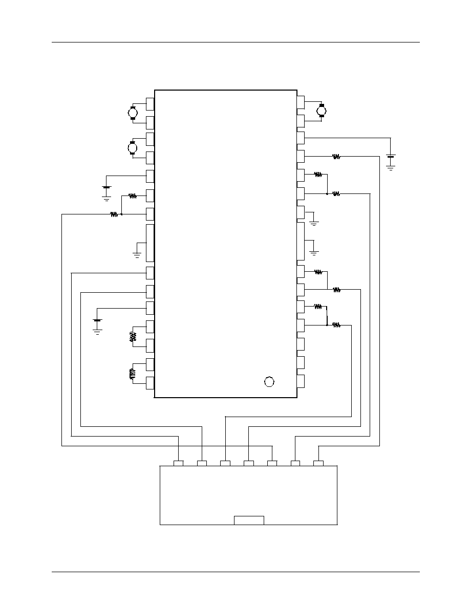
Typical Application Circuit
7
FI
N
OPIN+
OPIN-
OPOUT
REF
IN5
OUT5
IN1
GND
IN4
OUT4
IN2
OUT2
DO3+
DO3-
DO2-
DO2+
DO1-
DO1+
SVCC
OUT3
IN3
VM1
MUTE
VM2
DO4+
DO4-
DO5+
DO5-
F
A
N
8
026G
3
FI
N
1
2
3
4
5
6
7
8
9
10
11
12
13
14
15
16
17
18
19
20
21
22
23
24
25
26
27
28
M
Focus
Actuat
or
Trackin
g
Actuato
r
Spindl
e
Motor
M
M Sled
Motor
Loadin
g
Motor
SERVO
FO
C
U
S
TR
A
C
K
I
N
G
SPIN
D
L
E
SL
ED
LO
A
D
IN
G
VR
E
F
5 V
8 V
MU
T
E
5 V

FAN8026G3
12
Test Circuits
1
2
3
4
5
6
7
8
9
10
11
12
13
14
FIN
28
27
26
25
24
23
22
21
20
19
18
17
16
15
FIN
OP
I
N
+
OP
IN
-
OP
O
U
T
IN
5
OUT5
IN4
OU
T4
GN
D
IN2
OUT
4
IN
1
VM
1
DO3
+
DO3
-
DO
2-
DO
2
+
DO1
-
DO
1+
SV
C
C
OU
T
3
IN3
RE
F
VM
2
MUTE
DO4
+
DO4
-
DO5
+
DO
5
-
FAN8026G3
A
A
A
V
SW3
A
A
A
A
V
SW2
V
SW
1
OP-AMP
IN+
IN-
OUT
A
A
A
A
V
SW
5
V
SW4
v
SW6
SW7
SW9
OP-AMP
IN+
IN-
OUT
SW8
A
A
A

FAN8026G3
13
Package Dimension
28-SSOPH-375-SG2

FAN8026G3
3/17/04 0.0m 001
Stock#DSxxxxxxxx
2004 Fairchild Semiconductor Corporation
LIFE SUPPORT POLICY
FAIRCHILD'S PRODUCTS ARE NOT AUTHORIZED FOR USE AS CRITICAL COMPONENTS IN LIFE SUPPORT DEVICES
OR SYSTEMS WITHOUT THE EXPRESS WRITTEN APPROVAL OF THE PRESIDENT OF FAIRCHILD SEMICONDUCTOR
CORPORATION. As used herein:
1. Life support devices or systems are devices or systems
which, (a) are intended for surgical implant into the body,
or (b) support or sustain life, and (c) whose failure to
perform when properly used in accordance with
instructions for use provided in the labeling, can be
reasonably expected to result in a significant injury of the
user.
2. A critical component in any component of a life support
device or system whose failure to perform can be
reasonably expected to cause the failure of the life support
device or system, or to affect its safety or effectiveness.
www.fairchildsemi.com
DISCLAIMER
FAIRCHILD SEMICONDUCTOR RESERVES THE RIGHT TO MAKE CHANGES WITHOUT FURTHER NOTICE TO ANY
PRODUCTS HEREIN TO IMPROVE RELIABILITY, FUNCTION OR DESIGN. FAIRCHILD DOES NOT ASSUME ANY
LIABILITY ARISING OUT OF THE APPLICATION OR USE OF ANY PRODUCT OR CIRCUIT DESCRIBED HEREIN; NEITHER
DOES IT CONVEY ANY LICENSE UNDER ITS PATENT RIGHTS, NOR THE RIGHTS OF OTHERS.