 | –≠–ª–µ–∫—Ç—Ä–æ–Ω–Ω—ã–π –∫–æ–º–ø–æ–Ω–µ–Ω—Ç: FAN8034 | –°–∫–∞—á–∞—Ç—å:  PDF PDF  ZIP ZIP |
©2000 Fairchild Semiconductor International
www.fairchildsemi.com
Rev. 1.0.1
Features
∑ 5-CH balanced transformerless (BTL) driver
∑ 1-CH (forward-reverse) control DC motor driver
∑ Operating supply voltage (4.5 V ~ 13.2 V)
∑ Built-in thermal shut down circuit (TSD)
∑ Built-in channel mute circuit
∑ Built-in power save mode circuit
∑ Built-in TSD monitor circuit
∑ Built-in 2-OP AMPs
Description
The FAN8034 is a monolithic integrated circuit suitable for
a 6-ch motor driver which drives the tracking actuator, focus
actuator, sled motor, spindle motor, and tray motor of the
CDP/CAR-CD/DVDP systems.
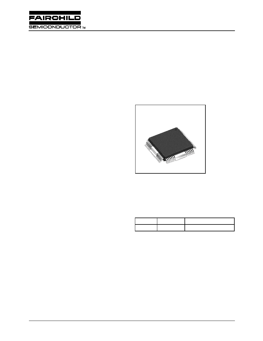
48-QFPH-1414
Typical Application
∑ Compact disk player
∑ Video compact disk player
∑ Car compact disk player
∑ Digital video disk player
Ordering Information
Device
Package
Operating Temperature
FAN8034
48-QFPH
-
35
∞
C ~ +85
∞
C
FAN8034
6-CH Motor Driver
FAN8034
2
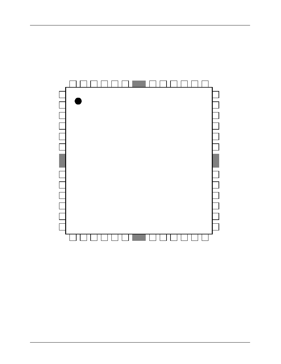
Pin Assignments
1
2
3
4
5
6
7
8
9
27
26
25
13
14
15
16
17
18
19
20
21
22
23
24
48
47
46
45
44
43
42
41
40
39
38
37
30
29
28
33
32
31
36
35
34
FAN8034
IN1
-
OUT1
IN2+
IN2
-
OUT2
IN3+
IN3
-
OUT3
10
11
12
DO2
-
PGND1
DO3+
DO3
-
DO4+
DO4
-
DO5+
DO5
-
PGND2
DO6+
IN
1
+
SV
CC
VR
E
F
PVCC1
DO
1
+
DO1
-
DO2+
SGND
PS
MUTE1
2
PVCC2
DO6
-
IN4+
IN4
-
OUT4
IN5+
IN
5
-
OUT5
FW
D
REV
CTL
MUTE3
4
MUT
E
5
TSD-
M
OP
I
N
1+
OP
I
N
1
-
OPOUT
1
OPI
N
2+
OP
I
N
2
-
OPOUT
2
FIN
(GND)
FIN
(GND)
FIN
(GND)
FIN
(GND)

FAN8034
3
Pin Definitions
Pin Number
Pin Name
I/O
Pin Function Descrition
1
IN1
-
I
CH1 op-amp input (
-
)
2
OUT1
O
CH1 op-amp output
3
IN2+
I
CH2 op-amp input (+)
4
IN2
-
I
CH2 op-amp input (
-
)
5
OUT2
O
CH2 op-amp output
6
IN3+
I
CH3 op-amp input (+)
7
IN3
-
I
CH3 op-amp input (
-
)
8
OUT3
O
CH3 op-amp output
9
IN4+
I
CH4 op-amp input (+)
10
IN4
-
I
CH4 op-amp input (
-
)
11
OUT4
O
CH4 op-amp output
12
IN5+
I
CH5op-amp input (+)
13
IN5
-
I
CH5 op-amp input (
-
)
14
OUT5
O
CH5 op-amp output
15
CTL
I
CH6 motor speed control
16
FWD
I
CH6 forward input
17
REV
I
CH6 reverse input
18
SGND
-
Signal ground
19
MUTE12
I
Mute for CH1,2
20
MUTE34
I
Mute for CH3,4
21
MUTE5
I
Mute for CH5
22
TSD-M
O
TSD monitor
23
PVCC2
-
Power supply voltage 2 (For CH5, CH6)
24
DO6
-
O
CH6 drive ouptut (
-
)
25
DO6+
O
CH6 drive output (+)
26
PGND2
-
Power ground 2 (FOR CH5, CH6)
27
DO5
-
O
CH5 drive ouptut (
-
)
28
DO5+
O
CH5 drive output (+)
29
DO4
-
O
CH4 drive ouptut (
-
)
30
DO4+
O
CH4 drive output (+)
31
DO3
-
O
CH3 drive ouptut (
-
)
32
DO3+
O
CH3 drive output (+)

FAN8034
4
Pin Definitions (Continued)
Pin Number
Pin Name
I/O
Pin Function Descrition
33
PGND1
-
Power ground 1 (For CH1, CH2, CH3, CH4)
34
DO2
-
O
CH3 drive ouptut (
-
)
35
DO2+
O
CH3 drive output (+)
36
DO1
-
O
CH3 drive ouptut (
-
)
37
DO1+
O
CH3 drive output (+)
38
PVCC1
-
Power supply voltage 1 (For CH1, CH2, CH3, CH4)
39
PS
I
Power save
40
OPOUT2
O
Normal op-amp2 output
41
OPIN2
-
I
Normal op-amp2 input (
-
)
42
OPIN2+
I
Normal op-amp2 input (+)
43
VREF
I
Bias voltage input
44
SVCC
-
Signal & OPAMPs supply voltage
45
OPOUT1
O
Normal op-amp1 output
46
OPIN1
-
I
Normal op-amp1 input (
-
)
47
OPIN1+
I
Normal op-amp1 input (+)
48
IN1+
I
CH1 op-amp intput (+)
FAN8034
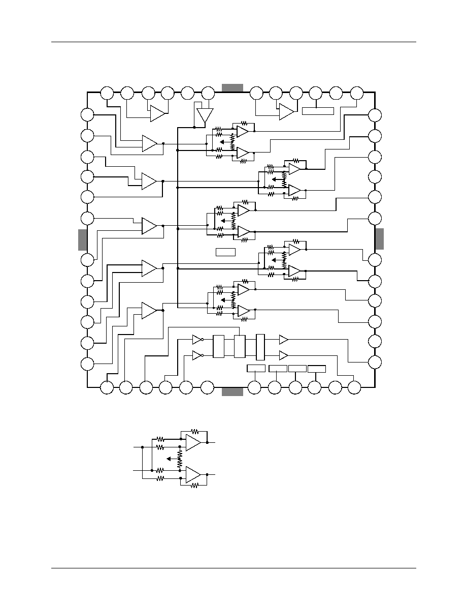
5
Internal Block Diagram
-
+
+
-
+
-
+
-
+
-
+
-
PGND1
DO2+
DO2
-
DO3+
DO3
-
DO4+
DO4
-
PGND2
DO5+
DO5
-
DO6+
1
2
3
4
5
6
7
8
9
10
11
12
IN1+
IN1
-
OUT1
IN2+
IN2
-
OUT2
IN3+
IN3
-
OUT3
13
14
15
16
17
18
19
20
21
22
23
24
SGND
TSD-M PVCC2 DO6
-
25
26
27
28
29
30
31
32
33
34
35
36
37
38
39
40
41
42
43
44
45
46
47
48
DO1
-
DO1+
PVCC1
VREF
SVCC
OPIN1
-
OPIN1+
T.S.D
MUTE12
POWER SAVE
-
+
OPOUT1
OPIN2
-
OPIN2+
OPOUT2 PS
IN4+
IN4
-
OUT4
IN5+
IN5
-
OUT5
CTL
FWD
REV
+
-
MUTE5
MUTE34
MUTE12
+
-
+
-
+
-
+
-
+
-
+
-
+
-
+
-
+
-
+
-
MUTE34 MUTE5 TSD-M
40K
10K
FIN
(GND)
FIN
(GND)
FIN
(GND)
FIN
(GND)
Note.
+
-
+
-
40K
10K
Pref
DO+
DO-
Detailed circuit of the output power amp
10K
10K
40K
40K
Pref1 is almost PVCC1 / 2
Pref2 is almost PVCC2 / 2
From input opamp
Vref
S
W
M
S
C
-
+
D
D

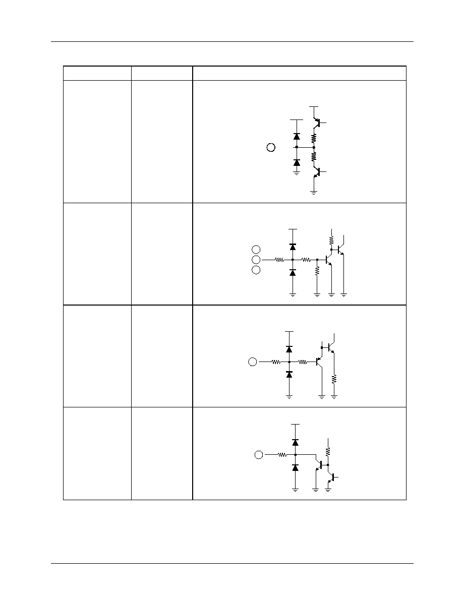
FAN8034
6
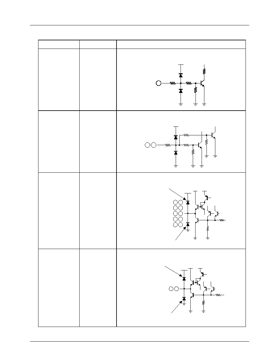
Equivalent Circuits
Description
Pin No
Internal Circuit
BTL INPUT
1,4,7,10,13,46
3,6,9,12,47,48
OP AMP INPUT
41,42
VREF
43
OUTPUT
2,5,8,11,14,45
VCC
VCC
2K
2K
6
3
9
12
47
48
4
1
7
10
13
46
VCC
5K
5K
41
42
VCC
43
1K
1K
5K
VCC
VCC
VCC VCC
5
11
45
2
8
14
FAN8034
7
Equivalent Circuits
Description
Pin No
Internal Circuit
OP OUT
40
MUTE1234
19, 20, 21
MUTE5
21
TSD-M
22
VCC
VCC
40
0.05k
0.05k
VCC
20
50K
50K
20K
19
21
21
VCC
1K
39K
22
20k
FAN8034
8
Equivalent Circuits
Description
Pin No
Internal Circuit
PS
39
FWD,REV
16,17
OUTPUT
27,28,29,30,31,
32,34,35,36,37
OUTPUT
24,25
50K
50K
100k
39
VCC
VCC
17
30K
30K
16
30K
30K
VCC
40
7K
VCC
28
30
32
35
37
27
29
31
34
36
40K
vcc
parastic diode
freewheeling diode
vcc
parastic diode
freewheeling diode
VCC
7K
VCC
60K
25
24
FAN8034
9
Absolute Maximum Ratings ( Ta=25
∞
∞
∞
∞
C)
Notes:
1. When mounted on 70mm
◊
70mm
◊
1.6mm PCB
2. Power dissipation reduces 24mW/
∞
C for using above T
A
= 25
∞
C
3. Do not exceed P
D
and SOA
Recommended Operating Conditions ( Ta=25
∞
∞
∞
∞
C)
Parameter
Symbol
Value
Unit
Maximum supply voltage
SVCC
MAX
18
V
PV
CC1
18
V
PV
CC2
18
V
Power dissipation
P
D
3
note
W
Operating temperature
T
OPR
-
35 ~ +85
∞
C
Storge temperature
T
STG
-
55 ~ +150
∞
C
Maximum output current
I
OMAX
1
A
Parameter
Symbol
Min.
Typ.
Max.
Unit
Operating supply voltage
SV
CC
4.5
-
13.2
V
PV
CC1
4.5
-
13.2
V
PV
CC2
4.5
-
13.2
V
3,000
2,000
1,000
0
0
25
50
75
100
125
150
175
Pd (mW)
Ambient temperature, Ta [
∞
C]

FAN8034
10
Electrical Characteristics
(SV
CC
=5V, PV
CC1
= PV
CC2
= 11V, T
A
= 25
∞
C, unless otherwise specified)
Note:
1. when the voltage of the pin39 is below 0.5V then Power save circuit cuts off the main bias current, so that the
whole circuts are disabled.
(whole circuits are "drive circuit ", " input op amp circuit " and " normal op amp circuit ")
Parameter
Symbol
Conditions
Min.
Typ.
Max.
Unit
Quiescent circuit current
I
CC
Under no-load
-
30
-
mA
Power save on current
*note
I
PS
Under no-load
-
-
1
mA
Power save on voltage
V
PSON
Pin39=Variation
-
-
0.5
V
Power save off voltage
V
PSOFF
Pin39=Variation
2
-
-
V
Mute12 on voltage
V
MON12
Pin19=Variation
-
-
0.5
V
Mute12 off voltage
V
MOFF12
Pin19=Variation
2
-
-
V
Mute34 on voltage
V
MON34
Pin20=Variation
-
-
0.5
V
Mute34 off voltage
V
MOFF34
Pin20=Variation
2
-
-
V
Mute5 on voltage
V
MON5
Pin21=Variation
-
-
0.5
V
Mute5 off voltage
V
MOFF5
Pin21=Variation
2
-
-
V
BTL DRIVER CIRCUIT
Output offset voltage
V
OO
V
IN
=2.5V
-
100
-
+100
mV
Maximum output voltage 1
V
OM1
R
L
=10
7.5
9.0
-
V
Maximum output voltage 2
V
OM2
R
L
=18
8.5
9.5
-
V
Closed-loop voltage gain
A
VF
V
IN
=0.1Vrms
16.8
18
19.2
dB
Ripple rejection ratio
RR
V
IN
=0.1Vrms, f=120Hz
-
60
-
dB
Slew rate
SR
Square, Vout=4Vp-p
1
2
-
V/
µ
s
INPUT OPAMP CIRCUIT
Input offset voltage 1
V
OF1
-
-
10
-
+10
mV
Input bias current 1
I
B1
-
-
-
400
nA
High level output voltage 1
V
OH1
-
4.4
4.7
-
V
Low level output voltage 1
V
OL1
-
-
0.2
0.5
V
Output sink current 1
I
SINK1
R
L
=50
1
2
-
mA
Output source current 1
I
SOU1
R
L
=50
1
2
-
mA
Common mode input range1
Vicm1
-
-0.3
-
4.0
V
Open Loop voltage gain 1
G
VO1
V
IN
=
-
75dB
-
80
-
dB
Ripple rejection ratio 1
RR1
V
IN
=
-
20dB, f=120Hz
-
65
-
dB
Common mode rejection ratio 1
CMRR1
V
IN
=
-
20dB
-
80
-
dB
Slew rate 1
SR1
Square, Vout=3Vp-p
-
1.5
-
V/
µ
s

FAN8034
11
Electrical Characteristics (Continued)
(SV
CC
= 5V, PV
CC1
= PV
CC2
= 11V, T
A
= 25
∞
C, unless otherwise specified)
Parameter
Symbol
Conditions
Min.
Typ.
Max.
Unit
NORMAL OP AMP CIRCUIT 1
Input offset voltage 2
V
OF2
-
-
10
-
+10
mV
Input bias current 2
I
B2
-
-
-
400
nA
High level output voltage 2
V
OH2
-
4.4
4.7
-
V
Low level output voltage 2
V
OL2
-
-
0.2
0.5
V
Output sink current 2
I
SINK2
R
L
=50
2
4
-
mA
Output source current 2
I
SOU2
R
L
=50
2
4
-
mA
Common mode input range 2
Vicm2
-
-0.3
-
4.0
V
Open loop voltage gain 2
G
VO2
V
IN
=
-
75dB
-
80
-
dB
Ripple rejection ratio 2
RR2
V
IN
=
-
20dB, f=120Hz
-
65
-
dB
Common mode rejection ratio 2
CMRR2
V
IN
=
-
20dB
-
80
-
dB
Slew Rate 2
SR2
Square, Vout=3Vp-p
-
1.5
-
V/
µ
s
NORMAL OP AMP CIRCUIT 2
Input offset voltage 3
V
OF3
-
-
15
-
+15
mV
Input bias current 3
I
B3
-
-
-
400
nA
High level output voltage 3
V
OH3
-
3
3.8
-
V
Low level output voltage 3
V
OL3
-
-
1.0
1.5
V
Output sink current 3
I
SINK3
R
L
=50
10
-
-
mA
Output source current 3
I
SOU3
R
L
=50
10
-
-
mA
Open loop voltage gain 3
G
VO3
V
IN
=
-
75dB
-
80
-
dB
Ripple rejection ratio 3
RR3
V
IN
=
-
20dB, f=120Hz
-
65
-
dB
Common mode rejection ratio 3
CMRR3
V
IN
=
-
20dB
-
80
-
dB
Slew rate 3
SR3
Square, Vout=3Vp-p
-
1.5
-
V/
µ
s
TRAY DRIVE CIRTUIT
Input High Level Voltage
V
IH
-
2
-
-
V
Input Low Level Voltage
V
IL
-
-
-
0.5
V
Output voltage 1
V
O1
PV
CC2
=11V, V
CTL
=3V,
R
L
=45
-
6
-
V
Output voltage 2
V
O2
PV
CC2
=13V, V
CTL
=4.5V,
R
L
=45
-
9
-
V
Output load regulation
V
RL
V
CTL
=3V, I
L
=100mA
400mA
-
300
700
mV
Output offset voltage 1
V
OO1
V
IN
=5V, 5V
-
40
-
+40
mV
Output offset voltage 2
V
OO2
V
IN
=0V, 0V
-
40
-
+40
mV

FAN8034
12
Application Information
1. Thermal Shutdown
∑ When the chip temperature reaches to 160
∞
C by abnormal condition, then the TSD circuit is activated.
∑ This shut down the bias current of the output drivers, and all the output drivers are in cut-off state. Thus the chip
temperature begin to decrease.
∑ when the chip temperature falls to 135
∞
C, the TSD circuit is deactivated and the output drivers are normally operated.
∑ The TSD circuit has the hysteresis temperature of 25
∞
C.
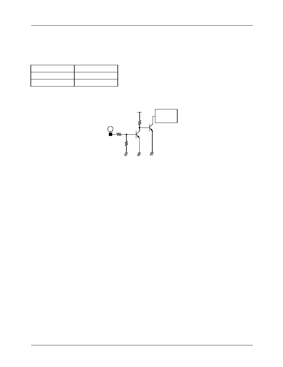
2. Ch Mute Function
∑ When the pin19,20,21 is high, the TR Q1 is turned on and Q2 is off, so the bias circuit is enabled. On the other hand, when
the pin19,20,21 is Low (GND) , the TR Q1 is turned off and Q2 is on, so the bias circuit is disabled.
∑ That is, this function will cause all the output drivers to be in mute state.
∑ Truth table is as follows;
Pin19,20,21
FAN8034
HIGH
Mute-off
LOW
Mute-on
SVCC
R2
R3
Q0
Output driver
bias
Hysteresis
R1
Ihys
I
REF
22
Q1
Bias blocks
(5-Ch BTL
and 1-Ch logic
loading)
Q2
SVCC
FAN8034
13
3. Power Save Function
∑ When the pin39 is high, the TR Q3 is turned on and Q4 is off, so the bias circuit is enabled. On the other hand, when the
pin39 is Low (GND) , the TR Q3 is turned off and Q4 is on, so the bias circuit is disabled.
∑ That is, this function will cause all the circuit blocks of the chip except for OPAMP to be in the off state. thus the low power
quiescent state is established
∑ Truth table is as follows;
Pin39
FAN8034
HIGH
Power Save Off
LOW
Power Save On
21
Q3
SVCC
Q4
Main Bias
FAN8034
14
4. Tsd Monitor Function
∑ PIN22 is TSD monitor pin which detects the state of the TSD block and generates the TSD-monitor signal.
∑ In normal state Q5 is turned on, so Q6 is turned off. on the otherhand, When the TSD block is is activated then Q5 is turned
off, so the voltage of pin22 is low.
∑ Truth table is as follows
5. Focus, Tracking Actuator, Spindle, Sled Motor Drive Part
∑ The voltage, Vref is the reference voltage given by the external bias voltage of the pin 43.
∑ The input signal (Vin) through pins 1,4,7, 10 and 13 is amplified one time and then fed to the output stage.
(assume that input opamp was used as a buffer)
∑ The total closed loop voltage gain is as follows
∑ If you want to change the total closed loop voltage gain, you must use the input opamp as an amplifier
∑ The output stage is the balanced transformerless (BTL) driver.
∑ The bias voltage Vp is expressed as ;
Tsd Circuit
pin22
FAN8034
-
HIGH
Tsd Off
-
LOW
Tsd On
43
Vref
48
3
6
+
-
+
-
9
+
-
OPin+
OPin-
Vp
Vp
M
R1
R2
R2
R2
R2
R1
R1
R2
DOP
DON
+
-
PVCC1(PVCC2)
60k
62k
Dp
Qp
Vin
39
38
37 34 32
31
33
36
12
1
4
7
10 13
48
3
6
9
12
Vin
Vref
V
+
=
DOP
Vp 4 V
+
=
DON
Vp 4
≠
V
=
Vout
DOP DON
8 V
=
≠
=
Gain
20
Vout
V
-------------
log
20
8
log
18dB
=
=
=
Vp
PVCC1 VDp
≠
VcesatQp
≠
(
)
62k
60k 62k
+
--------------------------
◊
VcesatQp
+
=
PVCC1 VDp
≠
VcesatQp
+
1.97
---------------------------------------------------------------------------
=
VcesatQp
+
- - - - - - - - - - (1)
FAN8034
15
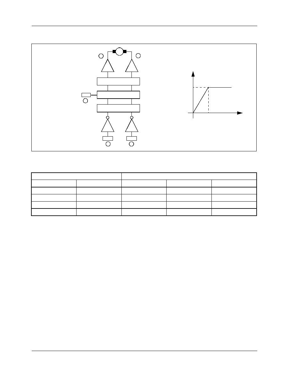
6. Tray, Changer,panel Motor Drive Part
∑ Rotational direction control
The forward and reverse rotational direction is controlled by FWD (pin16) and REV (pin17) and the input conditions are as
follows.
∑ Where Vp(Power reference voltage) is approximately about 3.75V at PVCC2=8V ) according to equation (1).
∑ Where out1 pins are pins24 and out2 pins are pins25
∑ Motor speed control (When SVCC=PVCC2=8V)
- The almost maximum torque is obtained when the pin (15(CTL1, 2, 3)) is open.
- If the voltage of the pins (15 (CTL)) is 0V, the motor will not operate.
- When the control voltage of the pin15 is between 0 and 3.25V, the differential output voltage(V(out1,out2)) is about two
times of control voltage. Hence, the control to the differential output gain is two.
- When the control voltage is greater than 3.25V, the output voltage is saturated at the 6.5V because of the output swing
limitation.
INPUT
OUTPUT
FWD
REV
OUT 1
OUT 2
State
H
H
Vp
Vp
Brake
H
L
H
L
Forward
L
H
L
H
Reverse
L
L
-
-
Hign impedance
M
24
25
out 1
out 2
D
LEVEL SHIFT
M.S.C
S.W
D
CTL
IN
FWD
REV
IN
16
17
15
V(out1,out2)
V
CTL
0
6.5V
3.25V
FAN8034
16
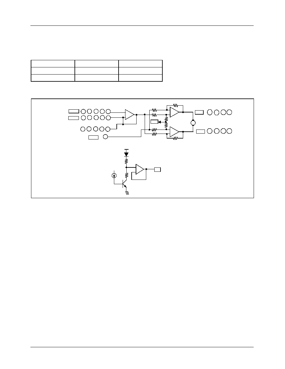
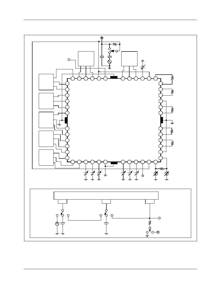
Test Circuits
37
38
39
40
41
42
43
44
45
46
47
48
9
10
11
12
8
7
6
5
4
1
2
3
13
14
15
16
17
18
19
20
21
22
23
24
25
26
27
28
31
32
33
34
35
36
OP IN (+)
OP IN (-)
OP OUT
CTL
OPIN(+)
OPIN(
-
)
OPOUT
FAN8034
IN2+
IN2-
OUT2
IN3+
IN3
-
OUT3
IN4+
IN4
-
OUT4
OPI
N
1
+
FW
D
REV
SG
N
D
TS
D
_
M
CTL
PS
MUT
E
12
PVC
C2
DO6
-
DO6+
PGND1
DO5
-
DO5+
DO4
-
DO4+
DO3
-
DO3+
PGND2
29
30
OP IN (+)
OP IN (-)
OP OUT
OP IN (+)
OP IN (-)
OP OUT
OP IN (+)
OP IN (-)
OP OUT
DO2-
INA INB
VREF
2.5
V
A
1
2
3
V
PULSE
V
A
B
1
2
3
V
B
C
D
50
V
CC
1
2
V
OUT
OP
-
AMP
PART
R
L7
I
L
I
L
OUT1
IN1
-
IN
1
+
SVCC
VR
E
F
PVC
C1
DO1+
DO1
-
DO2+
OPI
N
1
-
OPOUT1
OPI
N
2+
OPI
N
2
-
OPOUT2
IN5+
IN
5
-
OUT5
MUT
E
34
MUT
E
5
R
L1
R
L2
R
L3
R
L4
R
L5
OP IN (+)
OP IN (-)
OP OUT
O
P
IN
(+)
O
P
IN
(
-
)
OP OUT
O
P
IN
(
-
)
O
P
IN
(
+
)
OP OUT
+
100
µ
F
+
1
2
50
1000
µ
F
V
CC
RIPPLE
FAN8034
17
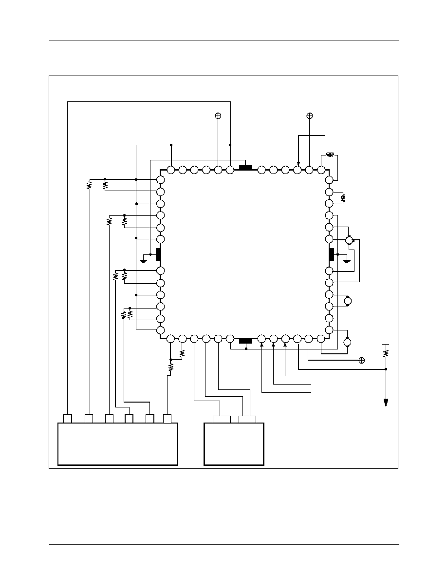
Typical Application Circuits 1
[Voltage control mode]
1
2
3
4
5
6
7
8
9
10
11
12
13
14
15
16
17
18
19
20
21
22
23
24
25
26
27
28
29
30
31
32
33
34
35
36
37
38
39
40
41
42
43
44
45
46
47
48
M
TRAY
CONTROL
TRAY
INPUT
VREF
FOCUS
INPUT
TRACKING
INPUT
SLED
INPUT
[SERVO PRE AMP]
[CONTROLLER]
Where TY is tray motor.
CG is changer motor
FAN8034
M
FOCUS, TRACKING,
MUTE
SLED
SPINDLE
TRACKI
NG
FOCUS
SPINDLE MUTE
M TRAY
PL is panel motor
IN2+
IN2-
OUT2
IN3
-
OUT3
IN4+
IN4
-
OUT4
OPI
N
1+
FW
D
REV
SGND
MUTE5
CTL
PS
MUTE12
PVCC2
DO6
-
DO6+
PGND1
DO5
-
DO5+
DO4
-
DO4+
DO3
-
DO3+
PGND2
DO2-
IN
1
+
SVCC
VREF
PVCC1
DO1
+
DO1
-
DO2+
OPI
N
1
-
OPOUT1
OPI
N
2
+
OPI
N
2
-
OPOUT2
IN
5
-
OUT
5
MUTE3
4
TSD_M
IN3+
OUT1
IN1
-
SLED MUTE
POWER SAVE
SPINDLE
INPUT
IN5+
TSD MONITOR
SVCC
PVCC1
PVCC2
pvcc2
FAN8034
18
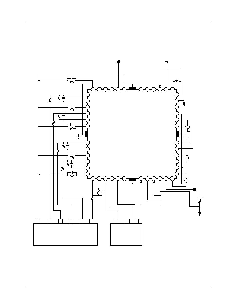
Typical Application Circuits 2
[Differential PWM control mode ]
Notes:
1. Radiation pin is connected to the internal GND of the package.
2. Connect the pin to the external GND
1
2
3
4
5
6
7
8
9
10
11
12
13
14
15
16
17
18
19
20
21
22
23
24
25
26
27
28
29
30
31
32
33
34
35
36
37
38
39
40
41
42
43
44
45
46
47
48
M
TY
CONTROL
TRAY
INPUT
VREF
FOCUS
INPUT
TRACKING
INPUT
SLED
INPUT
SPINDLE
INPUT
[SERVO PRE AMP]
[CONTROLLER]
Where TY is tray motor.
CG is changer motor
FAN8034
POWER SAVE
FOCUS, TRACKING
MUTE
TRAY
SPINDLE
T
R
ACKI
NG
FOCUS
SPINDLE MUTE
M
PL is panel motor
IN2+
IN2-
OUT2
IN3
-
OUT3
IN4+
IN4
-
OUT4
OPI
N
1+
FW
D
REV
SGND
TS
D
_
M
CTL
PS
MUTE1
2
PVCC2
DO6
-
DO6+
PGND1
DO5
-
DO5+
DO4
-
DO4+
DO3
-
DO3+
PGND2
DO2-
IN
1
+
SVCC
VREF
PVCC1
DO1+
DO1
-
DO2+
OPI
N
1
-
OPOUT1
OPI
N
2
+
OPI
N
2
-
OPOUT2
IN
5
-
OUT5
MUTE3
4
MUTE5
IN3+
OUT1
IN1
-
IN5+
SLED MUTE
TSD MONITOR
M
SLED
SVCC
PVCC1
PVCC2
pvcc2

FAN8034
19

FAN8034
12/1/00 0.0m 001
Stock#DSxxxxxxxx
2000 Fairchild Semiconductor International
LIFE SUPPORT POLICY
FAIRCHILD'S PRODUCTS ARE NOT AUTHORIZED FOR USE AS CRITICAL COMPONENTS IN LIFE SUPPORT DEVICES
OR SYSTEMS WITHOUT THE EXPRESS WRITTEN APPROVAL OF THE PRESIDENT OF FAIRCHILD SEMICONDUCTOR
INTERNATIONAL. As used herein:
1. Life support devices or systems are devices or systems
which, (a) are intended for surgical implant into the body,
or (b) support or sustain life, and (c) whose failure to
perform when properly used in accordance with
instructions for use provided in the labeling, can be
reasonably expected to result in a significant injury of the
user.
2. A critical component in any component of a life support
device or system whose failure to perform can be
reasonably expected to cause the failure of the life support
device or system, or to affect its safety or effectiveness.
www.fairchildsemi.com
DISCLAIMER
FAIRCHILD SEMICONDUCTOR RESERVES THE RIGHT TO MAKE CHANGES WITHOUT FURTHER NOTICE TO ANY
PRODUCTS HEREIN TO IMPROVE RELIABILITY, FUNCTION OR DESIGN. FAIRCHILD DOES NOT ASSUME ANY
LIABILITY ARISING OUT OF THE APPLICATION OR USE OF ANY PRODUCT OR CIRCUIT DESCRIBED HEREIN; NEITHER
DOES IT CONVEY ANY LICENSE UNDER ITS PATENT RIGHTS, NOR THE RIGHTS OF OTHERS.