
©2001 Fairchild Semiconductor Corporation
www.fairchildsemi.com
Rev 1.0.1
Features
∑ 1 Phase, Full-wave, Linear DC Motor Driver
∑ Built-in 5-CH Balanced TransFormerless (BTL) Driver
∑ Built-in thermal shut down circuit (TSD)
∑ Built-in Variable Regulator With Power Tr.
∑ Built-in Power Save Circuit
∑ Built-in stand by mode circuit
∑ Wide Operating Supply Voltage : 4.5 ~ 13.2V
Description
The FAN8039BD3 is a monolithic integrated circuit suitable
for a 5-CH motor driver which drives the tracking actuator,
focus actuator, sled motor, tray motor, spindle motor of the
DVDP/CAR-CD systems.
28-SSOPH-375SG2
Typical Applications
∑ Compact disk player
∑ Video compact disk player
∑ Car compact disk player
∑ Mixing with compact disk player and mini disk player
∑ DVDP
Ordering Information
Device
Package
Operating Temp
FAN8039BD3
28-SSOPH-375SG2
-
3
5
∞
C ~ 8
5
∞
C
FAN8039BD3TF 28-SSOPH-375SG2
-
3
5
∞
C ~ 8
5
∞
C
FAN8039BD3
5-CH Motor Driver

5-CH MOTOR DRIVER
2
Pin Assignments
Pin Definitions
NO
Symbol
Description
NO
Symbol
Description
1
DO1-
CH1 Drive Output (-)
15
GND2
Power Ground1 (CH 2,3,5)
2
DO1+
CH1 Drive Output (+)
16
DO5+
CH5 Drive Output (+)
3
IN1
CH1 Drive Input
17
DO5-
CH5 Drive Output(-)
4
REGVCC
Regulator Supply Voltage
18
DO3-
CH3 Drive Output(-)
5
REB
Regulator Output
19
DO3+
CH3 Drive Output (+)
6
REO
Regulator Feedback Input
20
IN3
CH3 Drive Input
7
RESX
Regulator Reset
21
VCC1
Supply Voltage1(CH2,CH3,CH5)
8
GND1
Signal Ground
22
PS
Power Save
9
CTL
CH5 Motor Speed Control
23
VREF
Bias Voltage
10
FWD
CH5 Forward Input
24
VCC
Supply Voltage(CH1,CH4)
11
REV
CH5 Reverse Input
25
IN4
CH4 Drive Input
12
IN2
CH2 Drive Input
26
DO4+
CH4 Drive Output (+)
13
DO2+
CH2 Drive Output (+)
27
DO4-
CH4 Drive Output (-)
14
DO2-
CH2 Drive Output (-)
28
GND3
Power Ground2 (CH 1,4)
1
3
2
4
5
6
7
21
19
20
18
17
16
15
8
10
9
11
12
13
14
DO1- DO1+ IN1 REGVCC REB
REO
PS
GND1
FWD
IN2
DO2+ DO2-
GND2
REV
DO5+
DO5-
DO3-
DO3+
IN3
CTL
VCC1
VCC
VREF
RESX
IN4
DO4+
DO4-
GND3
FAN8039BD3
FAN8039BD3
FAN8039BD3
FAN8039BD3
28
26
27
25
24
23
22

5-CH MOTOR DRIVER
3
Internal Block Diagram
28
26
27
25
24
23
22
1
3
2
4
5
6
7
21
19
20
18
17
16
15
8
10
9
11
12
13
14
DO
1
-
DO
1
+
IN
1
REGVCC
REB
REO
RESX
GND
1
FWD
IN
2
DO
2
+
DO
2
-
GND
2
REV
DO
5
+
DO
5
-
DO
3
-
DO
3
+
IN
3
CTL
VCC
1
VCC
VREF
PS
IN
4
DO
4
+
DO
4
-
GND
3
TSD
10K
10K
10K
10K
2.5V
Regulator
Level
Shift
Level
Shift
COMP
2
2
2
2
2
2
FIN
(GND)
FIN
(GND)
Level
Shift
Level
Shift
10K
10K
Level
Shift
2
2
PS
RESX
FUNCTION
H
H
H
L
L
H
L
L
All Active
Reg. Only Deactive
Reg. Only Active
All Deactive

5-CH MOTOR DRIVER
4
Equivalent Circuits
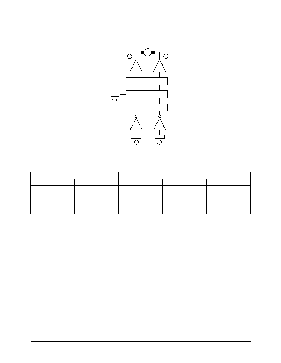
Btl Driver Output
Btl Drive Input
Regulator Output
Regulator Feedback Input
Regulator Reset
Motor Speed Control
2
13
14
1
17
18
19
16
30K
20K
12
20
25
25
3
5
20K
6
1K
25
7
50K
25
50K
20K
9
25
1k

5-CH MOTOR DRIVER
5
Equivalent Circuits
Forward Input
Reverse Input
Power Save
Bias Voltage
10
25
30K
30K
30K
30K
11
25
30K
30K
30K
30K
22
25
50K
50K
20K
23
25
0.5K

5-CH MOTOR DRIVER
6
Absolute Maximum Ratings (Ta = 25
∞
∞
∞
∞
C)
Notes:
1. When mounted on 70mm
◊
70mm
◊
1.6mm PCB
2. Power dissipation reduces 20mW/
∞
C for using above T
A
= 25
∞
C
3. Do not exceed P
D
and SOA (Safe Operating Area)
Recommended Operating Conditions
(Ta = 25
∞
∞
∞
∞
C)
Parameter
Symbol
Value
Unit
Maximum Supply Voltage
VCC
18
V
Power Dissipation
P
D
2.5
note
W
Operating Temperature
T
OPR
-
35 ~ +85
∞
C
Storge Temperature
T
STG
-
55 ~ +150
∞
C
Maximum output current
I
OMAX
1
A
Regulator Maximum output current
I
ROMAX
400
mA
Parameter
Symbol
Min.
Typ.
Max.
Unit
Operating Supply Voltage
Vcc
4.5
-
13.2
V
Vctl(pin9) Voltage(Vcc=Vcc1=8V)
Vctl
0
-
3.0
V
Vctl(pin9) Voltage(Vcc=Vcc1=5V)
Vctl
0
-
1.6
V
3,000
2,000
1,000
0
0
25
50
75
100
125
150
175
Pd (mW)
Ambient temperature, Ta [
∞
C]

5-CH MOTOR DRIVER
7
Electrical Characteristics
(V
CC
= V
CC1
= 8V, T
A
= 25
∞
C, unless otherwise specified)
Note:
1. Pulse Testing with Low Duty.
Characteristics
Symbol
Condition
Min.
Typ.
Max.
Unit
Quiescent Circuit Current
I
CCQ
Under no - load
-
20
-
mA
Power Save On Current
I
PS
Pin7=GND
-
1
2
mA
Power Save On Voltage
V
PSON
Pin7=Variation
-
-
0.5
V
Power Save Off Voltage
V
PSOFF
Pin7=Variation
2
-
-
V
VARIABLE REGULATOR PART
Load Regulation
V
RL
I
L
= 0mA
200mA
-40
0
10
mV
Line Regulation
V
CC
I
L
= 200mA, V
CC
=6V
9V
-20
0
30
mV
Regulator Output Voltage 1 V
REG1
I
L
= 100mA
4.75
5
5.25
V
Regulator Output Voltage 2 V
REG2
I
L
= 100mA
3.135
3.3
3.465
V
Regulator Output Peak
Current (Note1)
I
PK
Tj = 25
∞
C
700
mA
BLT DRIVER PART
Output Offset Voltage
V
OO
V
IN
=2.5V
-40
0
40
mV
Maximum Output Voltage1
V
OM1
V
CC
=Vcc1=8V, RL = 12
5.5
6.5
-
V
Maximum Output Voltage2
V
OM2
V
CC
=Vcc1=13V, RL = 24
10.5
11.5
-
V
Close Loop Voltage Gain
AV
F
V
IN
=0V, 1Vrms, f = 1KHz
10.5
12
13.5
dB
Slew rate
SR
V
OUT
=4V
P-P
, f = 120KHz, Square
-
2
-
V/
µ
s
LOADING MOTOR DRIVER PART
Input High Level Voltage
V
IH
-
2
-
-
V
Input Low Level Voltage
V
IL
-
-
-
0.5
V
Output Voltage1
Vo1
V
CC
=V
CC
1=5V, Vctl=1.8V,RL = 12
2.6
3.6
Output Voltage2
V
O2
V
CC
=V
CC
1=8V, Vctl=3.2V,RL = 12
5.5
6.5
-
V
Output Offset Voltage1
V
OO1
V
IN
=5V , 5V
-40
-
40
mV
Output Offset Voltage2
V
OO2
V
IN
=0V , 0V
-40
-
40
mV

5-CH MOTOR DRIVER
8
Application Information
1. Driver (Except For Loading Motor Driver)
A voltage, VREF is the reference voltage driven by the external bias voltage on pin#23. The input signal(Vin) on pin#12 and
#20 is uplifted by 10K/10K times and then fed to the level shift. The level shift provides a current as +
I and -
I due to the
difference between the input signal and the arbitrary reference signal. The current can be fed into the driver Amp, so it drives
the power TR on the output stage. The output can be shown 2 times as much as the input signal. (gain = 1 + 10K/10K).
Pin#3 or #25 can be used to modify the gain. The output stage is the balanced transformerless(BTL) driver.
The bias voltage VP is described as follows.
M
LEVEL
SHIFT
+
-
-
-
-
10K
10K
10K
10K
10K
10K
10K
10K
0.1K
60K
62K
2
2
2
2
13
13
13
13
19
19
19
19
26
26
26
26
1
1
1
1
18
18
18
18
14
14
14
14
27
27
27
27
DO+
DO-
VREF
23
23
23
23
20
20
20
20
25
25
25
25
12
12
12
12
3
3
3
3
VCC
V
P
I
I
-
V
IN
V
REF
V
I
V
10K
-----------
=
+
=
DO
V
P
I 10K
1 10K
10K
-----------
+
V
P
2
V
+
=
∑
∑
+
=
+
DO
V
P
I 10K
1 10K
10K
-----------
+
V
P
2
V
≠
=
∑
∑
≠
=
≠
V
OUT
DO+
(
)
DO-
(
)
4
V
=
≠
=
GAIN
20
V
OUT
V
--------------
12dB
=
log
=
V
P
VCC V
BE
V
CE SAT
(
)
≠
≠
(
)
62K
60K 62K
+
----------------------------
V
CE SAT
(
)
+
◊
=
VCC V
BE
≠
V
CE SAT
(
)
≠
1.97
-------------------------------------------------------------
V
CE SAT
(
)
+
=

5-CH MOTOR DRIVER
9
2. Thermal Shutdown
The TSD circuit turns activated when the junction temperature becomes
over 175
∞
C.
It cuts off the bias current on the output driver and keeps all the output
drivers off. Meanwhile, the junction temperature begins to decrease.
The TSD circuit can be deactivated when the unction temperature falls
under 150
∞
C, so the output driver begins operating in normal condition
The TSD circuit has the hysteresis temperature of 25
∞
C
.
3. Power Save Function
When the pin22 is high, the TR Q3 is turned on and Q4 is off, so the bias
circuit is enabled. On the other hand, when the pin22 is Low (GND) ,
the TR Q3 is turned off and Q4 is on, so the bias circuit is disabled.
that is, it will make all the circuit blocks except for variable regulator off,
so low power quiescent state can be established.
Truth table is as follows.
4. Variable Regulator
A 33uF capacitor is used as a ripple eliminator in the external cir-
cuit. Therefore, output voltage, Vout can be calculated as follows.
In order to reduce the heating problem on regulator output
TR,Q1, a resistor R3 can be used and calculated as follows
.
Pin#22
FAN8039BD3
High
Power Save Off
Low
Power Save On
VCC
R2
R3
Q0
Output driver
bias
Hysteresis
R1
Ihys
I
REF
22
Q3
Main Bias
(except for
variable reg.)
VCC
Q4
REGVCC
V
REF
V
OUT
R1
R2
33uF
2.5V
5
6
4
7
RESX
R3
Q1
I
MAX
V
OUT
V
REF
1
R
1
R
2
-------
+
∑
2.5 2
◊
5V R1
R2
=
(
)
=
=
=
R3
REGVCC
Vout 1.5
+
(
)
≠
(
)
IMAX
-----------------------------------------------------------------------
=
5-CH MOTOR DRIVER
10
5. Loading Motor Driver
∑ Rotational direction control
The forward and reverse rotational direction is controlled by FWD (pin10) and REV (pin11) , so the conditions are as
follows.
∑ Vp(Power Bias voltage) can be approximately 3.75V where Vcc1and Vcc are 8V.
∑ Vb(Brake Bias voltage) can be approximately 1.7V where Vcc1and Vcc are 8V.
∑ Motor speed control (Where VCC=VCC1=8V)
- The maximum torque can be obtained when the pin 9(CTL) is open.
- If the voltage on pin 9(CTL) is 0V, the motor will not be operating.
INPUT
OUTPUT
FWD
REV
OUT 1
OUT 2
State
H
H
Vp
Vp
Short Brake.
H
L
H
L
Forward
L
H
L
H
Reverse
L
L
Vb
Vb
High Impedance
M
13
14
DO2+
DO2-
D
LEVEL SHIFT
M.S.C
S.W
D
CTL
IN
FWD
REV
IN
10
11
9

5-CH MOTOR DRIVER
11
Typical Performance Characteristics
VCTL vs. VO CURVE
0.0
2.0
4.0
6.0
8.0
0
1
2
3
4
5
VCTL[V]
VO[V]
Vcc=8V
load=10
Temp vs Ips
-0.1
0.1
0.3
0.5
0.7
0.9
1.1
1.3
1.5
-35
-10
15
40
65
Temp()
I
ps
(
m
A
)
Temp vs Avf
0
2
4
6
8
10
12
14
16
-35
-10
15
40
65
Temp()
A
vf(
d
B)
Temp vs
V
rl
-40
-30
-20
-10
0
10
-35
-10
15
40
65
Temp()
Vrl(
m
V)
Temp vs
V cc
-50
-40
-30
-20
-10
0
10
-35
-10
15
40
65
Temp()
Vcc(
m
V)
Temp vs V Reg1
4.75
4.85
4.95
5.05
5.15
5.25
-35
-10
15
40
65
Temp()
Reg
1
(V)
Vcc=8V
Vcc1=8V
Vcc=8V
Vcc1=8V
Vin=1kHz
Vcc=8V
Vcc1=8V
IL=0~200mA
IL=200mA
Vcc=5~9V
Vcc=8V
Vcc1=8V
IL=100mA

5-CH MOTOR DRIVER
12
Typical Performance Characteristics
(Continued)
V cc vs Icc
0
5
10
15
20
25
30
35
4.5
5.5
6.5
7.5
8.5
9.5
10.5 11.5 12.5
V cc(V )
I
cc(
m
A
)
V cc vs V om
0
2
4
6
8
10
12
14
4.5
5.5
6.5
7.5
8.5
9.5 10.5 11.5 12.5
V cc(V )
Vo
m
(V)
V cc vs Avf
10.5
11
11.5
12
12.5
13
13.5
4.5
6.5
8.5
10.5
12.5
V cc(V )
A
vf(
d
B)
V cc vs V reg
3
3.5
4
4.5
5
5.5
4
5
6
7
8
9
10
11
12
13
V cc(V )
Vreg(V)
Temp vs Icc
0
5
10
15
20
25
30
-35
-10
15
40
65
Temp()
I
cc(
m
A
)
Temp vs V om
0
1
2
3
4
5
6
7
-35
-10
15
40
65
Temp()
Vo
m
(V)
No Load
Vcc=8V
Vcc1=8V
RL=12V
Vcc=8V
Vcc1=8V
RL=12
Vcc=8V
Vcc1=8V
IL=100mA
No Load
Vcc=8V
Vcc1=8V
RL=12

5-CH MOTOR DRIVER
13
Test Circuit
28
26
27
25 24
23
22
1
3
2
4
5
6
7
21
19
20
18
17 16
15
8
10
9
11 12
13
14
DO1- DO1+ IN1 REGVCC REB REO
PS
GND1
FWD
IN2
DO2+ DO2-
GND2
REV
DO5+
DO5-
DO3-
DO3+
IN3
CTL
VCC1
VCC VREF
IN4
DO4+
DO4-
GND3
FAN8039BD3
FAN8039BD3
FAN8039BD3
FAN8039BD3
SW2
2
3
1
12
24
SW1
1
2
SW7
2
3
1
12 24
SW6
1
12
24
SW5
1
2
2
SW3
2
3
1
12
SW4
1
2
24
SW8
2
3
1
VCC
2.5V
+
+ 470uF
104
100uF
12
24
SW9
1
2
RESX
10K
10K

5-CH MOTOR DRIVER
14
Application Circuit
28
26
27
25
24
23
22
1
3
2
4
5
6
7
21
19
20
18
17
16
15
8
10
9
11
12
13
14
DO1- DO1+ IN1 REGVCC REB
REO
PS
GND1
FWD
IN2
DO2+ DO2-
GND2
REV
DO5+
DO5-
DO3-
DO3+
IN3
CTL
VCC1
VREF
IN4
DO4+
DO4-
GND3
FAN8039BD3
FAN8039BD3
FAN8039BD3
FAN8039BD3
M
100uF
Reg
out
P
S
FOCUS
LOADING
MOTOR
SLED
470uF 102
VCC
FORWARD
SPINDLE
SLED
BIAS
TRACKING
FOCUS
SERVO PRE-AMP
CONTROLLER
VCC
RESX
CONTROL
REVERSE
R
E
S
X
M
SPINDLE
M
TRACK

5-CH MOTOR DRIVER
15
Mechanical Dimensions
Package
28-SSOPH-375-SG2

5-CH MOTOR DRIVER
11/7/01 0.0m 001
Stock#DSxxxxxxxx
2001 Fairchild Semiconductor Corporation
LIFE SUPPORT POLICY
FAIRCHILD'S PRODUCTS ARE NOT AUTHORIZED FOR USE AS CRITICAL COMPONENTS IN LIFE SUPPORT DEVICES
OR SYSTEMS WITHOUT THE EXPRESS WRITTEN APPROVAL OF THE PRESIDENT OF FAIRCHILD SEMICONDUCTOR
CORPORATION. As used herein:
1. Life support devices or systems are devices or systems
which, (a) are intended for surgical implant into the body,
or (b) support or sustain life, and (c) whose failure to
perform when properly used in accordance with
instructions for use provided in the labeling, can be
reasonably expected to result in a significant injury of the
user.
2. A critical component in any component of a life support
device or system whose failure to perform can be
reasonably expected to cause the failure of the life support
device or system, or to affect its safety or effectiveness.
www.fairchildsemi.com
DISCLAIMER
FAIRCHILD SEMICONDUCTOR RESERVES THE RIGHT TO MAKE CHANGES WITHOUT FURTHER NOTICE TO ANY
PRODUCTS HEREIN TO IMPROVE RELIABILITY, FUNCTION OR DESIGN. FAIRCHILD DOES NOT ASSUME ANY
LIABILITY ARISING OUT OF THE APPLICATION OR USE OF ANY PRODUCT OR CIRCUIT DESCRIBED HEREIN; NEITHER
DOES IT CONVEY ANY LICENSE UNDER ITS PATENT RIGHTS, NOR THE RIGHTS OF OTHERS.