 | –≠–ª–µ–∫—Ç—Ä–æ–Ω–Ω—ã–π –∫–æ–º–ø–æ–Ω–µ–Ω—Ç: FAN8040G3 | –°–∫–∞—á–∞—Ç—å:  PDF PDF  ZIP ZIP |

©2004 Fairchild Semiconductor Corporation
www.fairchildsemi.com
Rev. 1.0.0
Features
∑ 4-channel Balanced Transformerless (BTL) Driver
∑ 3-channels PWM input direct-coupled type include
internal filters.
∑ Separated power supply voltages
(PVCC1: CH1 and CH2, PVCC2: CH3 and CH4)
∑ Built-in input pin selection function of channel 4
∑ Built-in OP-amplifier
∑ Built-in Power Save function
∑ Built-in Thermal Shutdown Circuit (TSD)
∑ Operating ranges: 4.5~ 13.2V
Description
The FAN8040G3 is a monolithic integrated circuit, suitable
for 4-channel motor driver which drives tracking actuator,
focus actuator, sled motor and spindle motor of compack
disk player system.
28-SSOPH-375-SG2
Typical Applications
∑ Compact Disk Player (CDP)
∑ Video Compact Disk Player (VCD)
∑ Other Compact Disk Media
Ordering Information
Device
Package
Operating
Temp.
FAN8040G3
28-SSOPH-375SG2
-40
∞C ~ +85∞C
FAN8040G3X
28-SSOPH-375SG2
-40
∞C ~ +85∞C
FAN8040
4-Channel Motor Driver

FAN8040
2
Pin Assignments
FAN8040G3
1
2
3
4
5
6
7
8
9
10
11
13
14
28
27
26
25
24
23
22
FIN
21
20
19
18
17
16
15
FIN
12
OPI
N
-
OP
IN
+
CH2OU
T
R
CH2OU
T
F
CH1OU
T
F
SW
CH
1FIN
CH
1R
IN
CH
2FIN
CH
2RIN
V
R
EFIN
PV
CC
1
GN
D
CH
1OUT
R
OP
O
U
T
OU
TV
R
E
F
C
H
3OUT
R
C
H
3OUT
F
CH
4C
AP
A
CH
4IN
PS
PV
C
C
2
C
H
4OUT
F
C
H
4OUT
R
VD
D
CH
3R
IN
GN
D
CH
3F
I
N

FAN8040
3
Pin Definitions
Pin Number
Pin Name
I/O
Pin Function Description
1
OPIN-
I
OP-amplifier negative input
2
OPIN+
I
OP-amplifier positive input
3
SW
I
channel 4 input change switch input
4
CH1FIN
I
Channel 1 PWM forward input
5
CH1RIN
I
Channel 1 PWM reverse input
6
CH2FIN
I
Channel 2 PWM forward input
7
CH2RIN
I
Channel 2 PWM reverse input
8
GND
-
Ground 1
9
VREFIN
I
Internal reference voltage input terminal
10
PVCC1
-
Power supply voltage for channel 1 and channel 2
11
CH2OUTR
O
Channel 2 reverse output
12
CH2OUTF
O
Channel 2 forward output
13
CH1OUTR
O
Channel 1 reverse output
14
CH1OUTF
O
Channel 1 forward output
15
CH4OUTR
O
Channel 4 reverse output
16
CH4OUTF
O
Channel 4 forward output
17
CH3OUTF
O
Channel 3 forward output
18
CH3OUTR
O
Channel 3 reverse output
19
PVCC2
-
Power supply voltage for channel 3 and channel 4
20
PS
I
Power save signal input
21
GND
-
Ground 2
22
CH3RIN
I
Channel 3 PWM reverse input
23
CH3FIN
I
Channel3 PWM forward input
24
CH4IN
I
Channel 4 input
25
CH4CAPA
I
Channel 4 external capacitor connection terminal
26
OUTVREF
I
Channel 4 external reference voltage input terminal
27
OPOUT
O
Op-amplifier output
28
VDD
-
Predriver power supply voltage

FAN8040
4
Internal Block Diagram
1
2
3
4
5
6
7
8
9
10
13
14
FIN
INTERFACE
R
11
12
PVCC1
(CH1,2)
OP
IN
-
OP
IN
+
CH
2O
U
T
R
C
H
2
OUT
F
CH
1OU
T
F
SW
CH
1F
IN
CH1R
IN
CH
2F
IN
CH
2R
IN
VREF
IN
PVCC1
GN
D
CH
1OU
T
R
28
27
25
24
23
22
FIN
21
20
19
16
15
Bias
Circuit
F
VDD
INTERFACE
R
F
INTERFACE
R
F
18
17
VDD
PVCC2
26
VDD
PVCC1
50K
50K
50K
50K
50K
50K
100K
100K
50K
10K
VDD
PVCC2
(CH3,4)
TSD
10K
19K
OP
O
U
T
OUTVREF
C
H
3
OUT
R
CH
3
O
U
T
F
CH
4CAPA
CH
4
I
N
PS
PV
CC2
C
H
4
OUT
F
CH
4
O
U
T
R
VD
D
CH
3RIN
GND
CH3FIN
D
D
D
5.3K
D
D
D
D
100K
25pF
100K
25pF
100K
25pF
F
R
R
F
F
R
D
PS CNTL
PS CNTL
D : Drive Buffer
SW : H--> ON, L --> OFF

FAN8040
5
Equivalent Circuits
Driver Forward Input
Driver Reverse Input
Driver Output
Internal Reference Voltage
PS Input
CH4 SW Input
17K
CH1, CH2 and CH3
23
6
4
22
17K
7
5
CH1, CH2 and CH3
11
30K
12
13
14
15
16
17
18
30K
9
50K
50K
20
50K
50K
3
2K
50K

FAN8040
6
Equivalent Circuits
(Continued)
OP- Amplifier Input
OP- Amplifier Output
External Reference Voltage Input
1
2
2K
2K
2K
2K
27
24
25
26
50K
50K
100K
100K
100K
100K
10K

FAN8040
7
Absolute Maximum Ratings (Ta = 25
∞C)
Note:
1. When mounted on a 76.2mm
◊ 114mm ◊ 1.57mm PCB (Phenolic resin material).
2. Power dissipation reduces 16.6mW/
∞C for using above Ta = 25∞C
3. Do not exceed P
D
and SOA (Safe operating area)
Power Dissipation Curve
Recommended Operating Condition (Ta = 25
∞C)
Parameter
Symbol
Value
Unit
Supply Voltage
PVCC1, 2
15
V
Predriver Supply Voltage
VDD
15
V
Power Dissipation
P
D
2.5
note
W
Operating Temperature
T
OPR
-40 ~ +85
∞C
Storage Temperature
T
STG
-55 ~ +150
∞C
Parameter
Symbol
Value
Unit
Operating Supply Voltage
PVCC1, 2
4.5 ~ 13.2
V
Predriver Supply Voltage
VDD
4.5 ~ 13.2
V
0
5 0 0
1 0 0 0
1 5 0 0
2 0 0 0
2 5 0 0
3 0 0 0
0
2 5
5 0
7 5
1 0 0
1 2 5
1 5 0
1 7 5
2 0 0
SOA
Ambient temperature, Ta[
∞C]
P
D
[mW]

FAN8040
8
Electrical Characteristics (Ta = 25
∞C)
(Ta=25
∞C, VDD=PVCC1=PVCC2=8V, R
L
=8
, f=1kHz, unless otherwise specified)
Note :
1. when the PS(pin20) is low level (under 0.5V) the bias circuit is disabled, so that the whole circuits are disabled.
2. Guranteed Design Value
Parameter
Symbol
Conditions
Min.
Typ.
Max.
Unit
Quiescent Circuit Current1
I
Q
Under no-load
-
17.0
25.0
mA
Internal Reference Input Voltage
V
REF
3.40
3.70
4.0
V
Quiescent Circuit Current2
(Note1)
I
PS
At Power Save On
-
10
100
uA
Power Save Off Voltage
V
PSOFF
2.0
-
-
V
Power Save On Voltage
V
PSON
-
-
0.5
V
BTL DRIVER PART (CH1, CH2 and CH3)
Input High Level Voltage
V
IH
2.4
-
VCC
V
Input Low Level Voltage
V
IL
-0.3
-
0.5
V
Input High Level Current
I
IH
V
F
=V
R
=5V
170
310
450
uA
Input Low Level Current (Forward)
I
ILF
V
F
=0V
-10
-
0
uA
Input Low Level Current (Reverse)
I
ILR
V
R
=0V
-50
-
0
uA
Output Offset Voltage
V
OO
-30
-
30
mV
Maximum Output Voltage
V
OM
V
F
=5V,V
R
=0V
4.4
5.0
5.6
V
Ripple Rejection Ratio
(Note2)
RR
VRR=100mVrms, 100Hz
-
70
-
dB
SPINDLE MOTOR DRIVER (CH4)
Input Bias Current
I
B
-
10
300
nA
Output Offset Voltage
V
OO4
CH4IN=OUTVREF
-50
-
50
mV
Maximum Output Voltage
V
OM
CH4IN=4V
4.8
5.4
-
V
Closed-loop Voltage Gain
GVC
9.3
11.3
13.3
dB
Ripple Rejection Ratio
(Note2)
RR
VRR=100mVrms, 100Hz
-
70
-
dB
ANALOG SWITCH INPUT
Input High Level Voltage
V
IHSW
2.0
-
VCC
V
Input Low Level Voltage
V
ILSW
-0.3
-
0.5
V
Input High Level Current
I
IHSW
VSW=3.5V
-
60
90
uA
Input Low Level Current
I
ILSW
VSW=0V
-10
0
10
uA
OP-AMPLIFIER
Offset Voltage
V
OFOP
-5
-
+5
mA
Input Bias Current
I
BOP
-
10
300
nA
Output High Level Volatage
V
OHOP
7.0
-
-
V
Output Low Level Volatage
V
OLOP
-
-
0.2
V
Output Sink Current
I
SINK
7.0
13.0
-
mA
Output Source Current
I
SOURCE
2.0
9.0
-
mA
Open-loop Voltage Gain
(Note2)
GVO
VIN=60dBV, 1KHz
-
65
-
dB
Slew Rate
(Note2)
SR
f=50KHz,2V
PP
(Squre)
-
0.5
-
V/us

FAN8040
9
Application Information
1. Power Save Function
∑ Power save function is also performed at PS (pin20). The truth table is as follows:
Figure 1. Truth table of Gain selection and Mute Function
∑ When the PS (pin 20) is hige level (above 2V), the bias circuit is enable. On the other hand, when the PS(pin20) is low level
(under 0.5V), the bias circuit is disabled.
∑ When the CAPA(pin3) is low level, the CAPA (pin25) is opened in Figure. 4.
2. TSD (Thermal Shutdown) Function
∑ When the chip temperature rises above 175
∞
C, then the 4-channels BTL driver output circuit will be muted.
The TSD circuit has the hysteresis temperature of 25
∞
C.
4. Balanced Transformerless(BTL) Driver (CH1, CH2 and CH3)
∑ CH1, CH2 and CH3 drive parts are composed of internal filter, V-I converter and output power amplifiers.
Figure 2. Schematic of BTL Driver (CH1, CH2 and CH3)
Table 1. Truth table of internal switches operation
SW (pin3)
PS (pin20)
Input
Function
Input
Function
L
CAPA(pin25) OFF
L
Power Save ON
H
CAPA(pin25) ON
H
Power Save OFF
VDD
Bias Circuit
20
PS CNTL
Buffer1
Buffer2
FWD
REV
OUT1
OUT2
F
PVCC
INTERFACE
R
S1
S2
I
1
I
2
R1=100K
C1=25
V
REF
A
F
R
S1
S2
L
L
OFF
OFF
L
H
OFF
ON
H
L
ON
OFF
H
H
ON
ON
H : above 2.4 [V]
L : under 0.5 [V]

FAN8040
10
∑ Internal primary filter is composed of sourcing/sinking current source of 25uA and forward/reverse controlled switches.
∑ It converts "FWD/REV" digital signals to analog signal as shown Figure. 2.
Figure 3. Operartion waveforms of BTL Driver (CH1, CH2 and CH3)
∑ If the forward input signal is high level (avobe 2.4V) and reverse input signal is low level (under 0.5V), then the forward
current source switch S1and reverse current source switch S2 become turn-on and turn-off, respectively.
∑ This causes the internal capacitor, C1, to be charged with sourcing current source of 25uA and consequently the voltage of
the filter output, V
A
, increases with the internal time constant of 2.5usec.
∑
∑ The time constant is
Where, R is 100 [
]
and C is 25[pF].
∑ The output voltages of power amplifers, V
OUTF
and V
OUTR
, are given as:
∑
Input
0V
0V
5V
FWD
REV
1V/usec
0V
V
REF
OUTF
OUTR
Output
Output
0V
V
REF
OUTF
OUTR
Input
0V
0V
5V
FWD
REV
)
]
[
5
.
2
:
(
],
[
5
.
2
1
1
V
input
reverse
Or
V
R
I
V
A
-
◊
=
sec]
[
5
.
2 u
C
R
=
◊
]
[
]
[
V
V
V
V
V
V
V
V
A
REF
OUTR
A
REF
OUTF
-
=
+
=

FAN8040
11
5. Channel 4 Driver (Spindle Motor Driver)
∑ The channel 4 driver is composed of input amplifer with input selection switch, V-I converter and output power amplifiers.
∑ The voltage, V
REF
, is the external reference voltage given by the bias voltage of the pin 26 in Figure. 4.
∑ The input signal, VIN, through the CH4IN (pin24) is amplified by 100K/100K times and then fed to the next amplifier. And
the amplified voltage is amplified by R2/R1 times and then the fed to the level shift circuit.
∑ Level shifit produces the current due to the difference between the input signal and the internal power reference (PVCC/2).
The current produced as +
I and -
I is fed into the driver buffer.
∑ If it is desired to change the gain, then the CH4CAPA (pin25) can be used. It is controlld by the SW (pin3) input signal.
∑ When the SW (pin3) is high level, then the input voltage,VIN, applied to the CH4CAPA (pin25).
Figure 4. Channel 4 Spindle Driver
24
3
V
REF
25
26
V
REF
R1
C1
C2
100K
100K
10K
5
0K
Servo Output
16
15
5
0K
5
0K
PVCC
D
D
Level
Shift
VREF
I
+
I
-
R1
R2
FAN8040
12
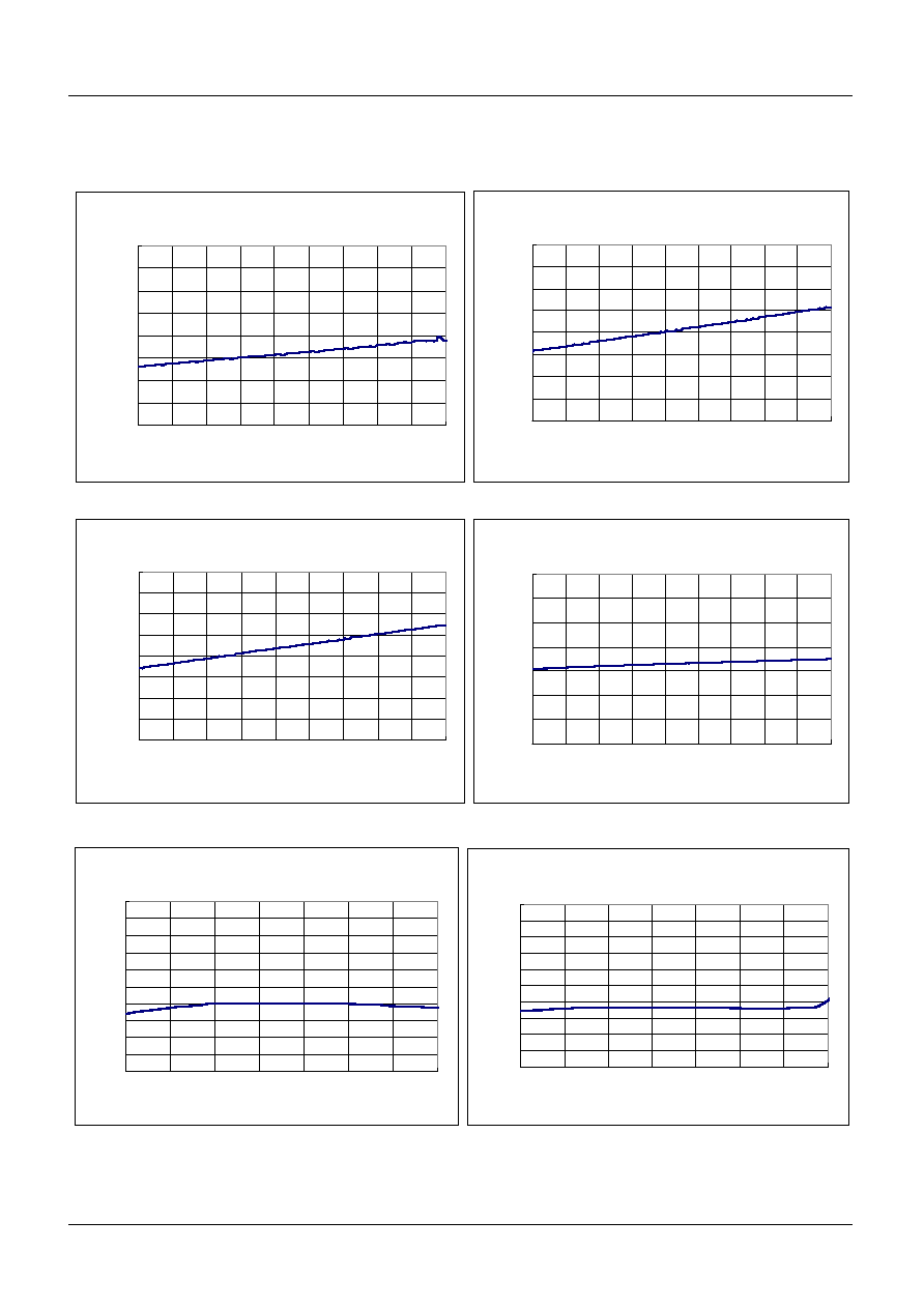
Typical Performance Characteristics
VDD vs IQ1
8
8.5
9
9.5
10
10.5
11
11.5
12
5
6
7
8
9
10
11
12
13
14
VDD[V]
IQ1[mA]
PVCC1 vs IPVCC1
0.2
0.25
0.3
0.35
0.4
0.45
0.5
0.55
0.6
5
6
7
8
9
10
11
12
13
14
PVCC1[V]
I
P
VCC1[
m
A]
PVCC2 vs IPVCC2
0.2
0.25
0.3
0.35
0.4
0.45
0.5
0.55
0.6
5
6
7
8
9
10
11
12
13
14
PVCC2[V]
IPV
C
C
1
[mA
]
VDD vs GCV
9.5
10
10.5
11
11.5
12
12.5
13
5
6
7
8
9
10
11
12
13
14
V DD[V ]
GCV[dB]
Temperature vs IQ1
5
6
7
8
9
10
11
12
13
14
15
-40
-20
0
20
40
60
80
100
Temp [∞C]
IQ1[mA]
Temperature vs IPVCC1
0
0.1
0.2
0.3
0.4
0.5
0.6
0.7
0.8
0.9
1
-40
-20
0
20
40
60
80
100
Temp [∞C]
IPVCC1[mA]

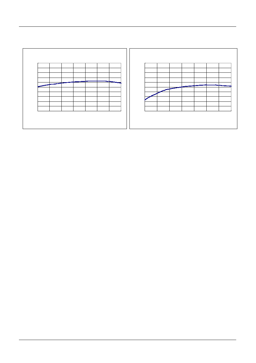
FAN8040
13
Temperatur vs IPVCC2
0
0.1
0.2
0.3
0.4
0.5
0.6
0.7
0.8
0.9
1
-40
-20
0
20
40
60
80
100
Temp [∞C]
IPVC2[mA]
Temperature vs VOM1AB
4
4.2
4.4
4.6
4.8
5
5.2
5.4
5.6
5.8
6
-40
-20
0
20
40
60
80
100
Temp [∞C]
VOM1AB[V]
Temperature vs VOM2AB
4
4.2
4.4
4.6
4.8
5
5.2
5.4
5.6
5.8
6
-40
-20
0
20
40
60
80
100
Temp[∞C]
VOM2AB[V
Temperature vs VOM3AB
4
4.2
4.4
4.6
4.8
5
5.2
5.4
5.6
5.8
6
-40
-20
0
20
40
60
80
100
Temp[∞C]
VOM3AB[V]
Temperature vs VOM4AB
4
4.2
4.4
4.6
4.8
5
5.2
5.4
5.6
5.8
6
-40
-20
0
20
40
60
80
100
Temp[∞C]
VOM4AB[V]
Temperature vs GCV1
9
9.5
10
10.5
11
11.5
12
12.5
13
-40
-20
0
20
40
60
80
100
Temp[∞C]
GCV1[dB]
FAN8040
14
Temperature vs ISOURCE
0
1
2
3
4
5
6
7
8
9
10
-40
-20
0
20
40
60
80
100
Temp[∞C]
IS
OURCE[mA]
Temperature vs ISINK
20
22
24
26
28
30
32
34
36
38
40
-40
-20
0
20
40
60
80
100
Temp[∞C]
IS
INK[mA]

FAN8040
15
Typical Application Circuits
M
M
1
2
3
4
5
6
7
8
9
10
13
14
FIN
INT
E
R
F
AC
E
R
11
12
PV
CC1
(C
H1,
2
)
28
27
25
24
23
22
FI
N
21
20
19
16
15
Bi
a
s
Ci
rcuit
F
PV
C
C
INTE
R
F
AC
E
R
F
INTE
R
F
AC
E
R
F
18
17
PVC
C
PV
CC
26
VDD
PVC
C
50K
50K
50K
50K
50K
50K
100K
1
00K
50K
1
0K
PV
CC
PV
CC
2
(C
H3,4
)
VR
E
F
TSD
10
K
19
K
D
D
D
D
5.3
K
D
D
D
D
10
0K
25pF
100K
25
pF
10
0K
25pF
FR
R
F
FR
PVCC
0.1uF
PVCC
0.1uF
VDD
0.1uF
0.47uF
300pF
82
15
Digital Servo
BIAS
1.75V
SPINDLE
Power
Save
FOR
W
ARD
REV
E
RSE
SLED
FOR
W
ARD
REV
E
RSE
FOCUS
FOR
W
ARD
REVERSE
TRACKING
H = ON
L = OFF
0.1uF
FOCUS
COIL
TRACKING
COIL
SPINDLE
MOTOR
SLED
MOTOR
FAN8040
16
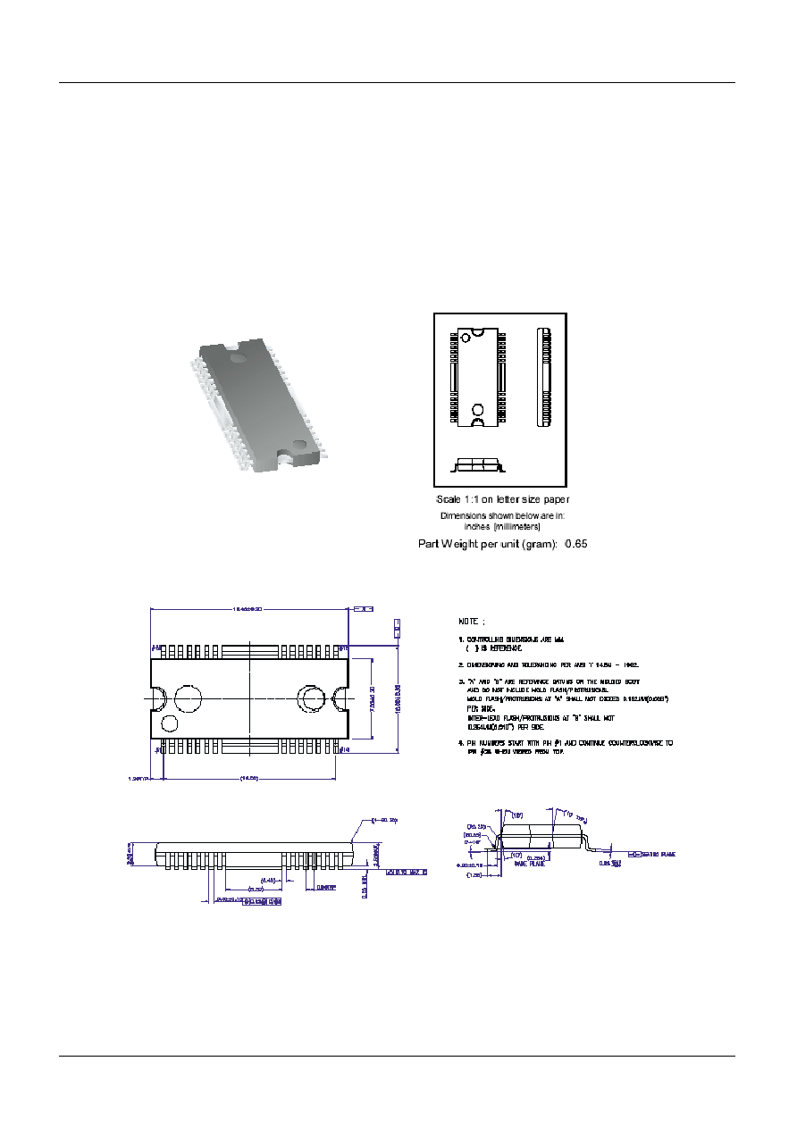
Mechanical Dimensions(Unit : mm)
Package Dimensions
28-SSOPH-375SG2

FAN8040
7/27/04 0.0m 001
Stock#DSxxxxxxxx
2004 Fairchild Semiconductor Corporation
LIFE SUPPORT POLICY
FAIRCHILD'S PRODUCTS ARE NOT AUTHORIZED FOR USE AS CRITICAL COMPONENTS IN LIFE SUPPORT DEVICES
OR SYSTEMS WITHOUT THE EXPRESS WRITTEN APPROVAL OF THE PRESIDENT OF FAIRCHILD SEMICONDUCTOR
CORPORATION. As used herein:
1. Life support devices or systems are devices or systems
which, (a) are intended for surgical implant into the body,
or (b) support or sustain life, and (c) whose failure to
perform when properly used in accordance with
instructions for use provided in the labeling, can be
reasonably expected to result in a significant injury of the
user.
2. A critical component in any component of a life support
device or system whose failure to perform can be
reasonably expected to cause the failure of the life support
device or system, or to affect its safety or effectiveness.
www.fairchildsemi.com
DISCLAIMER
FAIRCHILD SEMICONDUCTOR RESERVES THE RIGHT TO MAKE CHANGES WITHOUT FURTHER NOTICE TO ANY
PRODUCTS HEREIN TO IMPROVE RELIABILITY, FUNCTION OR DESIGN. FAIRCHILD DOES NOT ASSUME ANY
LIABILITY ARISING OUT OF THE APPLICATION OR USE OF ANY PRODUCT OR CIRCUIT DESCRIBED HEREIN; NEITHER
DOES IT CONVEY ANY LICENSE UNDER ITS PATENT RIGHTS, NOR THE RIGHTS OF OTHERS.