 | –≠–ª–µ–∫—Ç—Ä–æ–Ω–Ω—ã–π –∫–æ–º–ø–æ–Ω–µ–Ω—Ç: FAN8045G3 | –°–∫–∞—á–∞—Ç—å:  PDF PDF  ZIP ZIP |
©2003 Fairchild Semiconductor Corporation
www.fairchildsemi.com
Rev. 1.0.1
Features
∑ 4-CH Balanced Transformerless (BTL) Driver
∑ Optional Input (CH4,5) For Output CH4
∑ Operating Supply Voltage : 4.5 V ~ 14V
∑ Built-in Thermal Shut Down Circuit (TSD)
∑ Built-in Channel Mute Circuit
∑ Built-in 1-OP AMP
∑ TSD Monitering Function
Description
The FAN8045G3 is a monolithic integrated circuit suitable
for a 4-CH motor driver which drives a tracking actuator, a
focus actuator, a sled motor, a spindle motor, and a tray
motor of the CDP/CAR-CD/DVDP systems.
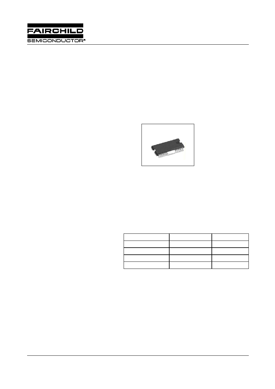
28-SSOPH-375SG2
FAN8045G3
4-CH Motor Driver (5 Input & 4 Output)
Typical Application
∑ Compact Disk Player
∑ Video Compact Disk Player
∑ Car Compact Disk Player
∑ Digital Video Disk Player
Ordering Information
Notes:
1. X : Tape&Reel
2. NL : Lead free
Device
Package
Operating Temp.
FAN8045G3
28-SSOPH-375-SG2
-35
∞C ~ +85∞C
FAN8045G3X
note1
28-SSOPH-375-SG2
-35
∞C ~ +85∞C
FAN8045G3_NL
note2
28-SSOPH-375-SG2
-35
∞C ~ +85∞C
FAN8045G3X_NL
28-SSOPH-375-SG2
-35
∞C ~ +85∞C

FAN8045G3
2
Pin Assignments
1
2
3
4
5
6
7
8
9
10
11
12
13
14
FIN
28
27
26
25
24
23
22
21
20
19
18
17
16
15
FIN
REF1
IN1
IN2
OPIN+
OPIN-
OPOUT
GND
PVcc1
MUTE
12
GND
DO2-
DO2+
DO1-
DO1+
DO4+
DO4-
DO3+
DO3-
GND
MUTE4
PVcc2
SVcc
IN3
IN4
REF2
IN5
MUTE3
SW45
FAN8045G3
FAN8045G3
3
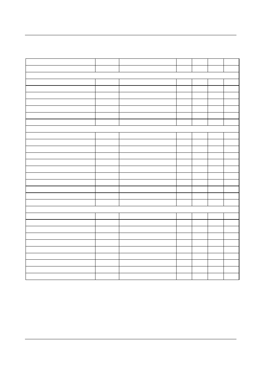
Pin Definitions
Pin Number
Pin Name
I/O
Pin Function Description
1
REF1
I
Bias Voltage Input
2
IN1
I
CH1 Input
3
IN2
I
CH2 Input
4
OPIN+
I
Nomal OP-AMP Input(+)
5
OPIN-
I
Nomal OP-AMP Input(-)
6
OPOUT
O
Nomal OP-AMP Output
7
GND
-
Signal Ground
8
PVcc1
-
Power Vcc (CH1,CH2)
9
MUTE12
I
Mute 1,2
10
GND
-
Power GND(CH1,CH2)
11
DO2-
O
CH2 Drive Output (-)
12
DO2+
O
CH2 Drive Output (+)
13
DO1-
O
CH1 Drive Output (-)
14
DO1+
O
CH1 Drive Output (+)
15
DO4+
O
CH4 Drive Output (+)
16
DO4-
O
CH4 Drive Output (-)
17
DO3+
O
CH3 Drive Output (+)
18
DO3-
O
CH3 Drive Output (-)
19
GND
-
Power GND(CH3,CH4)
20
MUTE4
I
Mute 4
21
PVcc2
-
Power Vcc (CH3,CH4)
22
SVcc
-
Signal Vcc
23
IN3
I
CH3 Input
24
IN4
I
CH4 Input
25
REF2
I
REF2
26
IN5
I
CH5 Input
27
MUTE3
I
Mute 3
28
SW45
I
Select Switch For 4,5CH
FAN8045G3
4
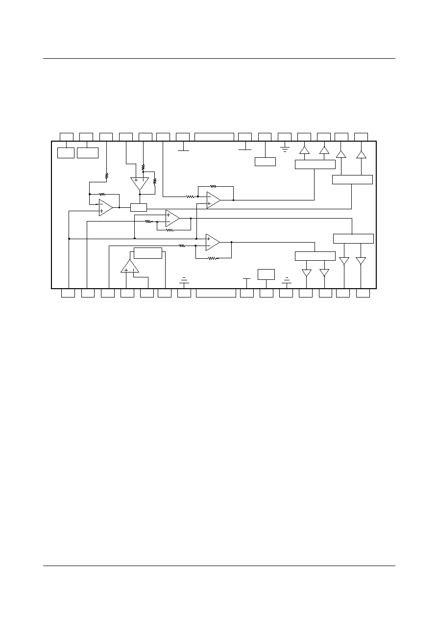
Internal Block Diagram
1
2
3
4
5
6
7
8
9
10
11
12
13
14
FIN
28
27
26
25
24
23
22
21
20
19
18
17
16
15
FIN
LEVEL SHIFT
LEVEL SHIFT
LEVEL SHIFT
LEVEL SHIFT
sw45
SW45
MUTE3
SVCC
PVCC2
MUTE4
GND
MUTE
12
PVCC1
GND
GND
10K
20K
10K
20K
20K
5K
20K
5K
5K
20K
REF1
IN1
IN2
OPIN+
OPIN-
OPOUT
GND
PVCC1
MUTE12
GND
DO2-
DO2+
DO1-
DO1+
DO4+
DO4-
DO3+
DO3-
GND
MUTE4
PVCC2
SVC
C
IN3
IN4
REF2
IN5
MUTE3
SW45
tsd
monitor

FAN8045G3
5
Equivalent Circuits
BTL Driver Output
SW45
BTL Input(CH1,2)
BTL Input(CH3,4)
Mute
Reference
20K
30K
11 12
13 14
15 16
17 18
SVCC PVCC
100K
100K
100K
100K
28
5K
2K
1K
2K
SVCC
2
3
10K
1K
1K
2K
2K
23
24
26
SVCC
50K
50K
9
20
27
50
50K
50K
1
25
FAN8045G3
6
Equivalent Circuits
(Continued)
OP-AMP Input
OP-AMP Output
2K
1K
1K
2K
2K
2K
SVCC
4
5
SVCC
6

FAN8045G3
7
Absolute Maximum Ratings ( Ta=25
∞C)
Notes:
1. When it is mounted on 70mm
◊ 70mm ◊ 1.6mm PCB.
2. Power dissipation decreases at the rate of 20mW/
∞C in T
A
>25
∞C.
3. Do not exceed P
D
and SOA.
Recommended Operating Conditions ( Ta=25
∞C)
Parameter
Symbol
Value
Unit
Maximum Supply Voltage
SVCC
MAX
18
V
PVCC1
MAX
18
V
PVCC2
MAX
18
V
Power Dissipation
P
D
2.5
note1,2,3
W
Operating Temperature
T
OPR
-35 ~ +85
∞C
Storge Temperature
T
STG
-55 ~ +150
∞C
Maximum Output Current
I
OMAX
1
A
Parameter
Symbol
Min.
Typ.
Max.
Unit
Operating Supply Voltage
SVCC
4.5
-
14
V
PVCC1
4.5
-
SVCC
V
PVCC2
4.5
-
SVCC
V
3,000
2,000
1,000
0
0
25
50
75
100
125
150
175
Pd (mW)
Ambient temperature, Ta [
∞C]
SOA
FAN8045G3
8
Electrical Characteristics
(SV
CC
= PV
CC2
= 12V, T
A
= 25
∞C,PV
CC1
= 5V , Ref1= 1.65V ,Ref2 = 2.5V , RL = 8
)
Note:
1.Guaranteed field. ( No EDS/ Final test . )
Parameter
Symbol
Conditions
Min.
Typ.
Max.
Unit
Quiescent Circuit Current
I
CC
Under no-load
-
17
25
mA
BTL DRIVER CIRCUIT (R
L=
8
)
Output Offset Voltage(CH12)
V
OOF1
V
IN
=1.65V
-50
-
+50
mV
Output Offset Voltage(CH34)
V
OOF2
V
IN
=1.65V
-100
-
+100
mV
Output Offset Voltage(CH5)
V
OOF3
V
IN
=2.5V
-100
-
+100
mV
Maximum Output Voltage(CH12)
V
OM1
PVcc1=5V, R
L
=8
3.6
4.0
-
V
Maximum Output Voltage(CH34)
V
OM2
PVcc2=12V, R
L
=24
9.6
10.5
-
V
Close-loop Voltage Gain(CH12)
A
VF
V
IN
= 0.3V
15.5
17.5
19.5
dB
Close-loop Voltage Gain(CH34)
A
VF
V
IN
= 0.3V
21.5
23.5
25.5
dB
NORMAL OPAMP CIRCUIT(SV
CC,
PV
CC2
=12V
)
Input Offset Voltage
V
OF
-
-10
-
+10
mV
Input Bias Current
I
B1
-
-
-
300
nA
High Level Output Voltage
V
OH1
-
11
-
-
V
Low Level Output Voltage
V
OL1
-
-
-
0.1
V
Output Sink Current
I
SINK
-
5
8
-
mA
Output Source Current
I
SOU1
-
1
5
-
mA
Open Loop Voltage Gain
G
VO1
f=1kHz, V
IN
= -75dB
-
75
-
dB
Ripple Rejection Ratio
note1
RR1
f=120Hz, V
IN
= -20dB
-
65
-
dB
Slew Rate
note1
SR1
f=120Hz, 2Vp-p
-
1
-
V/us
Common Mode Rejection Ratio
note1
CMRR1
f=1kHz, V
IN
= -20dB
-
80
-
dB
TSD ON Voltage
note1
Vtsdon
-
-
-
0.5
V
MUTE AND OTHER FUNCTION CIRCUIT
Mute On Voltage
V
MON
Pin9,20,27=Variation
-
-
0.5
V
Mute Off Voltage
V
MOFF
Pin9,20,27=Variation
2
-
-
V
SW On Voltage
V
SWL
Pin28=Variation
-
-
0.5
V
SW Off Voltage
V
SWH
Pin28=Variation
2
-
-
V
Mute Low Level Sink Current
IMTL
VMUTE = 0V
-15
0
15
uA
Mute High Level Sink Current
IMTH
VMUTE = 5V
-
85
170
uA
SW45 Low Level Sink Current
ISWL45
SW45 = 0V
-15
0
15
uA
SW45 High Level Sink Current
ISWH45
SW45 = 5V
-
85
170
uA
REF1 Sink Current
IRL
REF1 = 1.65V
-
52
104
uA
REF2 Sink Current
IRH
REF2 = 2.5V
-
85
170
uA
FAN8045G3
9
Application Information
1.
MUTE,REF & SW45 Function
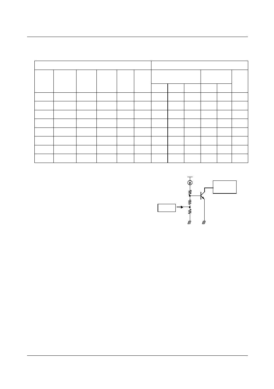
2. TSD Function
∑ When the chip temperature reaches to 167
∞C by abnormal condition,
the TSD circuit is activated
∑ During TSD Function is activated, OP-AMP Output (pin 6) remains
below 0.5V. (TSD monitoring function).
∑ This makes the bias current of the output drivers shut down, and all
the output drivers are on cut-off state. Therefore the chip temperature
begins to decrease.
∑ When the chip temperature falls to 63
∞C, the TSD circuit is
deactivated and the output drivers start to operate normally.
3. Notice
∑ If REF1(pin1) or REF2(pin25) is lower than 0.7V, BTL Output is off.
∑ Under Voltage Protecton Function. ( If SVcc is lower than 3.8V, Chip is disable. Hysterisis is 0.2V)
∑ Mute ON BTL OutPut Voltage is as followed:
- Mute ON BTL Output (CH1,2) = (PVcc1 ) / 2
- Mute ON BTL Output (CH3,4) = ((PVcc2-0.6) / 2
∑ Each output to output and output to GND short should be kept away.
INPUT
OUTPUT
SW45
MUTE12
MUTE3
MUTE4
REF1
REF2
BTL
PRE-AMP
OP
CH12
CH3
CH4
CH4
CH5
H
H
H
-
H
-
ON
ON
IN5
ON
ON
ON
H
H
L
-
H
-
ON
OFF
IN5
ON
ON
ON
H
H
H
-
L
-
OFF
OFF
OFF
OFF
ON
OFF
H
L
H
-
H
-
OFF
ON
OFF
ON
ON
ON
H
L
L
-
H
-
OFF
OFF
OFF
ON
ON
ON
L
-
-
L
-
-
OFF
OFF
OFF
OFF
ON
OFF
L
-
-
H
-
H
OFF
OFF
IN4
OFF
ON
OFF
L
-
-
H
-
L
OFF
OFF
OFF
OFF
ON
OFF
SVCC
R2
R3
Q0
Output driver
bias
Hysteresis
R1
Ihys
I
REF
FAN8045G3
10
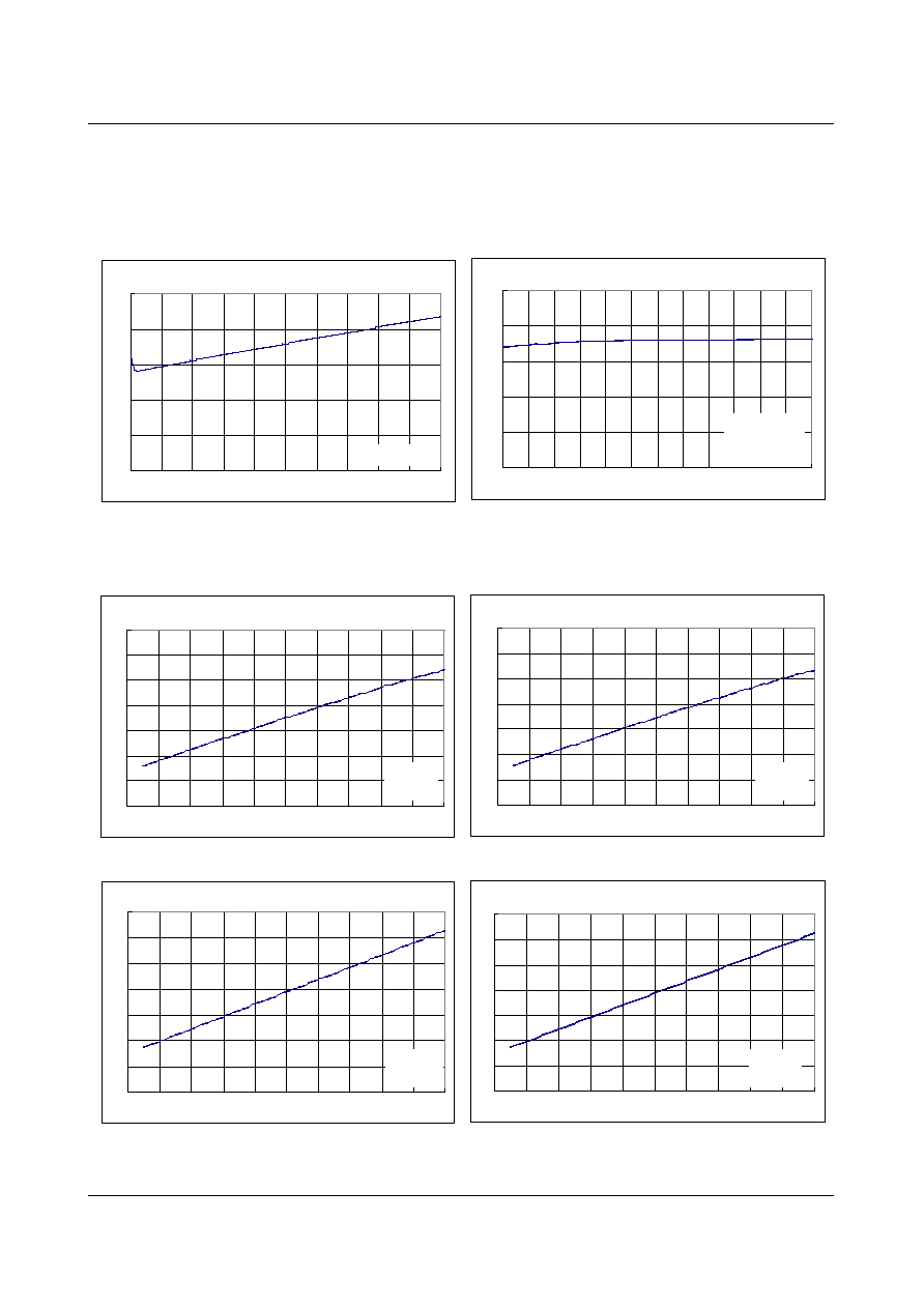
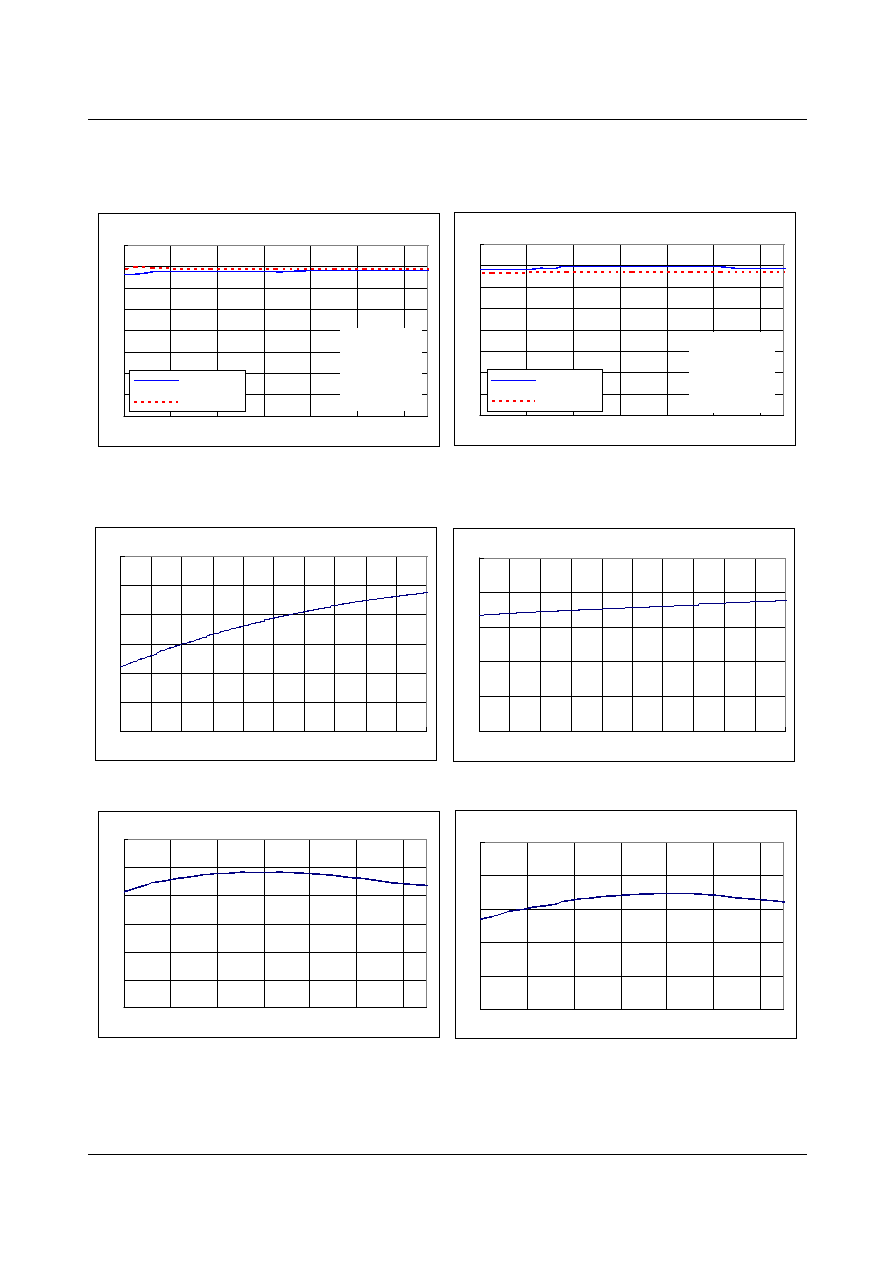
Typical Performance Characteristics
Total Circuit
Icc(mA)
Vcc(
V
)
<Vcc vs Icc1>
0
5
10
15
20
25
4.5
5.5 6.5
7.5 8.5
9.5 10.5 11.5 12.5 13.5 14.5
Temp=25
O
C
Temp(
∞
C)
Icc(mA)
<Temp vs Icc1>
0
5
10
15
20
25
-35 -25 -15 -5
5
15 25 35 45 55 65 75 85
SV cc=12V
PV cc2=12V
PV cc1=5V
BTL Drive Part
<Vcc vs Vom1>
0
2
4
6
8
10
12
14
4
5
6
7
8
9
10
11
12
13
14
V in=0V
RL=8
Vcc(
V
)
Vom(
V
)
<Vcc vs Vom2>
0
2
4
6
8
10
12
14
4
5
6
7
8
9
10
11
12
13
14
V in=0V
RL=8
Vom(
V
)
Vcc(
V
)
<Vcc vs Vom3>
0
2
4
6
8
10
12
14
4
5
6
7
8
9
10
11
12
13
14
V in=0V
RL=24
Vom(
V
)
Vcc(
V
)
<Vcc vs Vom4>
0
2
4
6
8
10
12
14
4
5
6
7
8
9
10
11
12
13
14
Vin=0V
RL=24
Vom(
V
)
Vcc(
V
)
FAN8045G3
11
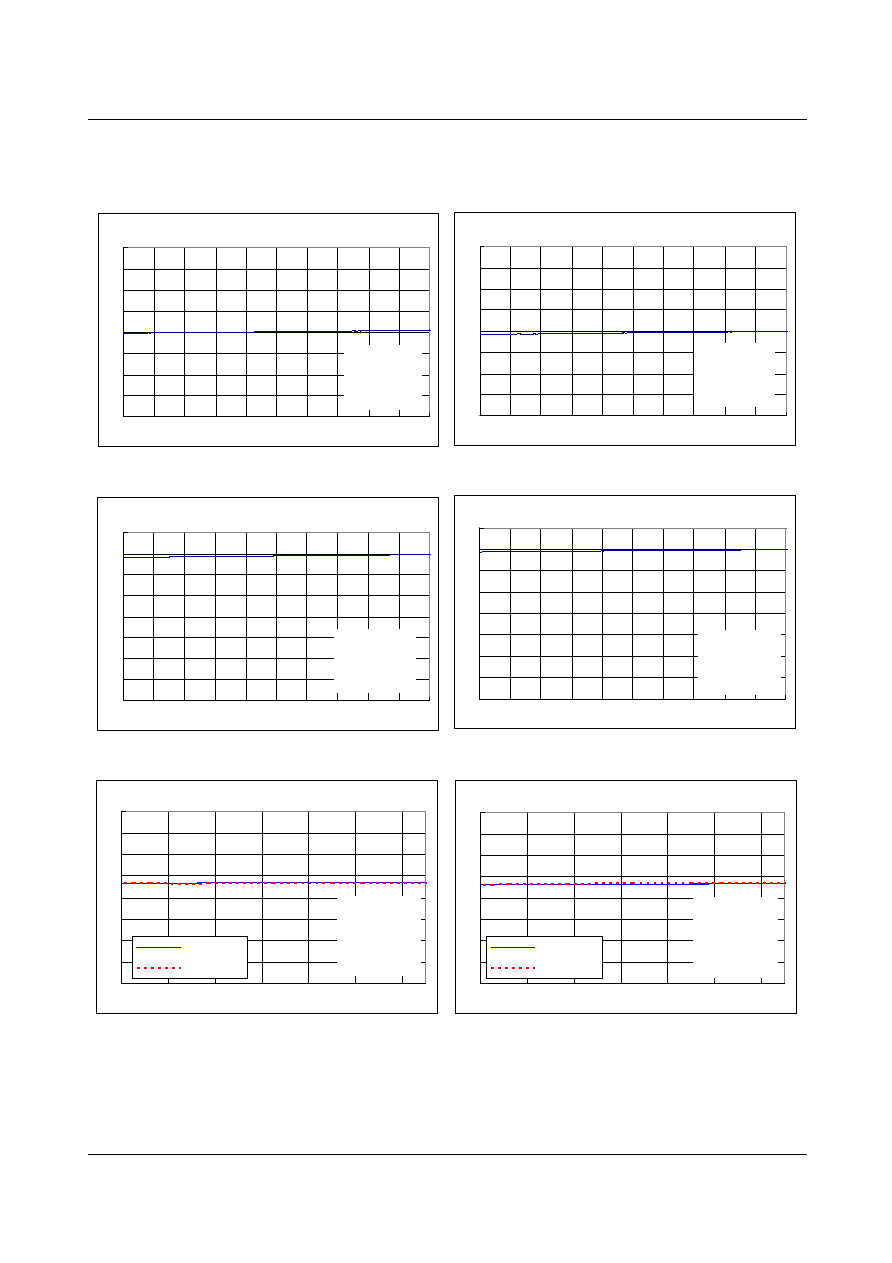
Typical Performance Characteristics
(Continued)
<Vcc vs Avf1>
10
12
14
16
18
20
22
24
26
4
5
6
7
8
9
10
11
12
13
14
Temp=25
O
C
V in=0.3V
Freg=1KHz
RL=8
Vcc(
V
)
Avf(
dB
)
<Vcc vs Avf2>
10
12
14
16
18
20
22
24
26
4
5
6
7
8
9
10
11
12
13
14
Temp=25
O
C
V in=0.3V
Freg=1KHz
RL=8
Vcc(
V
)
Avf(
dB
)
<Vcc vs Avf3>
10
12
14
16
18
20
22
24
26
4
5
6
7
8
9
10
11
12
13
14
Temp=25
O
C
V in=0.3V
Freg=1KHz
RL=24
Vcc(
V
)
Avf(
dB
)
<Vcc vs Avf4>
10
12
14
16
18
20
22
24
26
4
5
6
7
8
9
10
11
12
13
14
Temp=25
O
C
V in=0.3V
Freg=1KHz
RL=24
Vcc(
V
)
Avf(
dB
)
<Temp vs Avf1>
8
10
12
14
16
18
20
22
24
-40
-20
0
20
40
60
80
V in=+0.3V
V in=-0.3V
SV cc=12V
PV cc1=5V
PV cc2=12V
Freq=1KHz
RL=8
Temp(
∞
C)
Avf(
dB
)
<Temp vs Avf2>
8
10
12
14
16
18
20
22
24
-40
-20
0
20
40
60
80
V in=+0.3V
V in=-0.3V
SV cc=12V
PV cc1=5V
PV cc2=12V
Freq=1KHz
RL=8
Temp(
∞
C)
Avf(
dB
)
FAN8045G3
12
Typical Performance Characteristics
(Continued)
<Temp vs Avf3>
10
12
14
16
18
20
22
24
26
-40
-20
0
20
40
60
80
V in=+0.3V
V in=-0.3V
SV cc=12V
PV cc1=5V
PV cc2=12V
Freq=1KHz
RL=24
Avf(
dB
)
Temp(
∞
C)
<Temp vs Avf4>
10
12
14
16
18
20
22
24
26
-40
-20
0
20
40
60
80
V in=+0.3V
V in=-0.3V
SV cc=12V
PV cc1=5V
PV cc2=12V
Freq=1KHz
RL=24
Temp(
∞
C)
Avf(
dB
)
OP-AMP Part
<Vcc vs Isink>
0
10
20
30
40
50
60
4
5
6
7
8
9
10
11
12
13
14
Vcc(
V
)
Isink(
mA
)
<Vcc vs Isou>
0
2
4
6
8
10
4
5
6
7
8
9
10
11
12
13
14
Vcc(
V
)
Isou(
mA
)
<Temp vs Isink>
0
10
20
30
40
50
60
-40
-20
0
20
40
60
80
Isink(
mA
)
Vcc(
V
)
<Tem p vs Isou>
0
2
4
6
8
10
-40
-20
0
20
40
60
80
Isou(
mA
)
Vcc(
V
)

FAN8045G3
13
Test Circuits
1
2
3
4
5
6
7
8
9
10
11
12
13
14
FIN
28
27
26
25
24
23
22
21
20
19
18
17
16
15
FIN
REF1
IN1
IN2
OPIN+
OPIN-
OPOUT
GND
P
V
CC1
MUTE12
GND
DO2-
DO2+
DO1-
DO1+
DO4+
DO4-
DO3+
DO3-
GND
MUTE4
P
V
CC2
SVCC
IN3
IN4
REF2
IN5
MUTE3
SW45
FAN8045G3
A
A
A
A
A
A
V
SW3
A
A
A
A
A
V
SW4
V
SW1
V
SW2
A
OP-AMP
IN+
IN- OUT
v
SW6
SW7
SW9
OP-AMP
IN+
IN-
OUT
SW8

FAN8045G3
14
Typical Application Circuit
MUTE4
LOADIN
G
VREF2
SW45
1
2
3
4
5
6
7
8
9
10
11
12
13
14
FIN
28
27
26
25
24
23
22
21
20
19
18
17
16
15
FIN
REF1
IN1
IN2
OPIN+
OPIN-
OPOUT
GND
PVCC1
MUTE12
GND
DO2-
DO2+
DO1-
DO1+
DO4+
DO4-
DO3+
DO3-
GND
MUTE4
PVCC2
SVCC
IN3
IN4
REF2
IN5
MUTE3
SW45
FAN8045G3
M
M
0.1uF
12V
12V
0.1uF
5V
0.1uF
Focus
Actuator
Tracking
Actuator
Sled & Loading
Motor
Spindle
Motor
SPINDLE
SLED
MUTE3
VREF1
FOCUS
TRACK
I
N
G
MUTE12
SERVO
MICOM
FAN8045G3
15
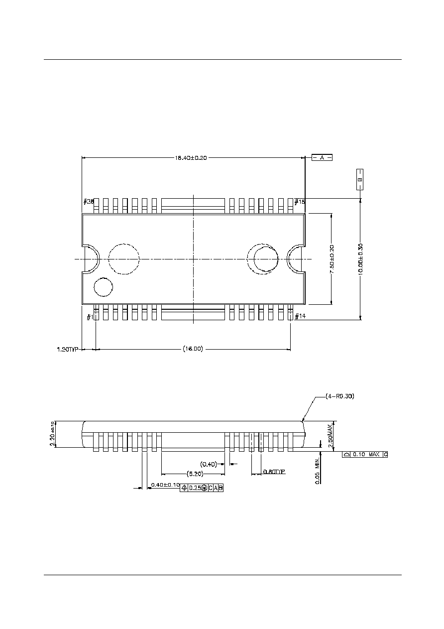
Package Dimension
28-SSOPH-375-SG2

FAN8045G3
3/15/03 0.0m 001
Stock#DSxxxxxxxx
2003 Fairchild Semiconductor Corporation
LIFE SUPPORT POLICY
FAIRCHILD'S PRODUCTS ARE NOT AUTHORIZED FOR USE AS CRITICAL COMPONENTS IN LIFE SUPPORT DEVICES
OR SYSTEMS WITHOUT THE EXPRESS WRITTEN APPROVAL OF THE PRESIDENT OF FAIRCHILD SEMICONDUCTOR
CORPORATION. As used herein:
1. Life support devices or systems are devices or systems
which, (a) are intended for surgical implant into the body,
or (b) support or sustain life, and (c) whose failure to
perform when properly used in accordance with
instructions for use provided in the labeling, can be
reasonably expected to result in a significant injury of the
user.
2. A critical component in any component of a life support
device or system whose failure to perform can be
reasonably expected to cause the failure of the life support
device or system, or to affect its safety or effectiveness.
www.fairchildsemi.com
DISCLAIMER
FAIRCHILD SEMICONDUCTOR RESERVES THE RIGHT TO MAKE CHANGES WITHOUT FURTHER NOTICE TO ANY
PRODUCTS HEREIN TO IMPROVE RELIABILITY, FUNCTION OR DESIGN. FAIRCHILD DOES NOT ASSUME ANY
LIABILITY ARISING OUT OF THE APPLICATION OR USE OF ANY PRODUCT OR CIRCUIT DESCRIBED HEREIN; NEITHER
DOES IT CONVEY ANY LICENSE UNDER ITS PATENT RIGHTS, NOR THE RIGHTS OF OTHERS.