©2001 Fairchild Semiconductor Corporation
www.fairchildsemi.com
Rev. 1.0.0
Features
∑ Built-in brake function for stable brake characteristics.
∑ Built-in element to absorb a surge current derived from
changing motor direction and braking motor drive.
∑ Motor speed control by an external voltage.
∑ Stable motor direction change.
∑ Interfaces with CMOS devices.
∑ Built-in the thermal shut down circuit (165
∞
C).
∑ Low standby current. (6.5mA)
Description
The FAN8082D is a monolithic integrated circuit designed
for driving bi-directional DC motor with braking and speed
control, and it is suitable for the loading motor driver of
VCR, CDP, and TOY systems. The speed control can be
achieved by adjusting the external voltage of the speed
control pin. It has two pins of logic inputs for controlling the
forward/ reverse and braking.
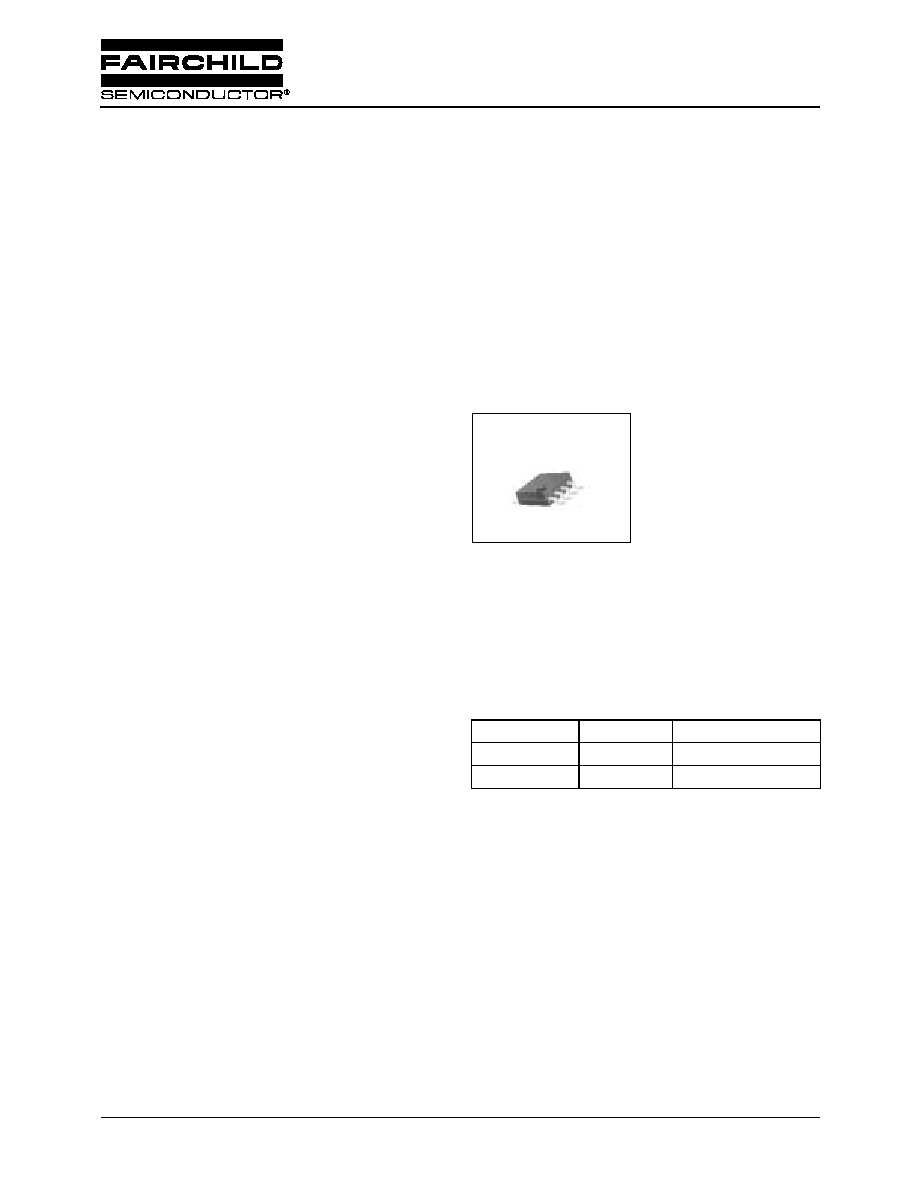
8-SOP-225
Typical Applications
∑ Compact disk player (CDP) tray or changer
∑ Low current DC motor such as audio or video equipment.
∑ General DC motor
Ordering Information
Device
Package
Operating Temp.
FAN8082D
8-SOP-225
-
25
∞
C ~ +75
∞
C
FAN8082DTF
8-SOP-225
-
25
∞
C ~ +75
∞
C
FAN8082D
Bi-directional DC Motor Driver
BI-DIRECTIONAL DC MOTOR DRIVER
2
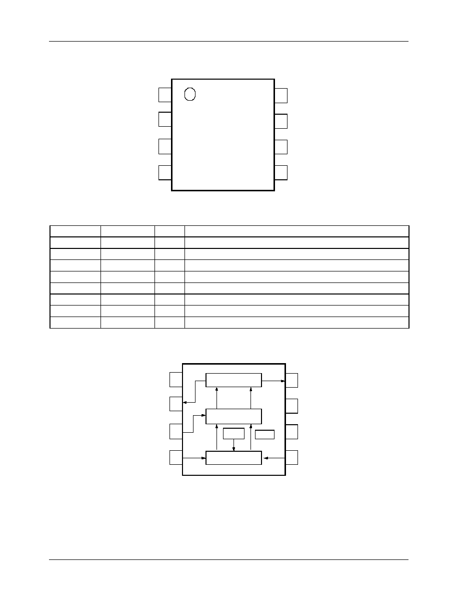
Pin Assignments
Pin Definitions
Internal Block Diagram
Pin Number
Pin Name
I/O
Pin Function Description
1
GND
-
Ground
2
V
O1
O
Output 1
3
V
CTL
I
Motor speed control
4
V
IN1
I
Input 1
5
V
IN2
I
Input 2
6
SV
CC
-
Supply voltage (Signal)
7
PV
CC
-
Supply voltage (Power)
8
V
O2
O
Output 2
1
2
5
6
7
8
GND
V
O1
V
CTL
V
IN1
V
IN2
SV
CC
PV
CC
V
O2
3
4
FAN8082D
DRIVER OUT
LOGIC SWITCH
1
2
5
6
7
8
GND
V
O1
V
CTL
V
IN1
V
IN2
SV
CC
PV
CC
V
O2
3
4
TSD
PRE DRIVER
BIAS
BI-DIRECTIONAL DC MOTOR DRIVER
3
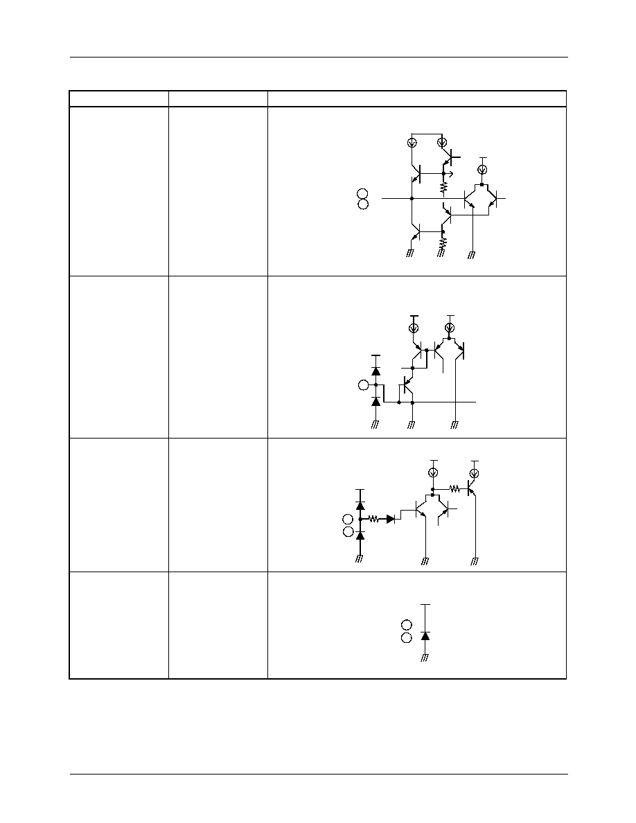
Equivalent Circuit
Description
Pin No.
Internal circuit
Output
2, 8
Speed control
3
Input
4, 5
SVCC
PVCC
6
7
2
8
Vcc
Vcc
VCC
3
Vcc
Vcc
VCC
4
5
Vcc
Vcc
VCC
6
7

BI-DIRECTIONAL DC MOTOR DRIVER
4
Absolute Maximum Ratings
(Ta = 25
∞
∞
∞
∞
C)
NOTES:
1. Duty 1 / 100, pulse width 500
µ
s
2. 1) When mounted on glass epoxy PCB (76.2
◊
114
◊
1.57mm)
2) Power dissipation reduces 2.64mW /
∞
C for using above Ta=25
∞
C.
3)
Do not exceed Pd and SOA(Safe Operating Area).
Power Dissipation Curve
Recommened Operating Conditions
(Ta = 25
∞
∞
∞
∞
C)
NOTE:
Caution 1) PV
CC
SV
CC
Caution 2) V
CTL
must be opened or 4.0
V
CTL
PV
CC
Parameter
Symbol
Value
Unit
Remark
Supply voltage
V
CCmax
13
V
-
Maxium Output current
I
Omax
0.8
note1
A
-
Power dissipation
P
d
330
note2
mW
-
Operating temperature
T
OPR
-
25 ~ +75
∞
C
-
Storage temperature
T
STG
-
55 ~ +125
∞
C
-
Parameter
Symbol
Operating voltage range
Unit
Operating supply voltage (Signal)
note
SV
CC
7 ~ 12
V
Operating supply voltage (Power)
note
PV
CC
4 ~ 8
V
330
0
0
25
50
75
100
125
Pd (mW)
Ambient temperature, Ta [
∞
C]
SOA
150
15

BI-DIRECTIONAL DC MOTOR DRIVER
5
Electrical Characteristics
(SVCC=PVCC=12V,Ta = 25
∞
∞
∞
∞
C)
Parameter
Symbol
Conditions
Min.
Typ.
Max.
Unit
Quiescent current
I
CC
Pin4 & 5: GND, R
L
=
4
6.5
9.5
mA
Min. input-on current 1
I
IN1
R
L
=
, Pin4=I
IN1
, Pin5=L
-
10
30
µ
A
Min. input-on current 2
I
IN2
R
L
=
, Pin4=L, Pin5=I
IN
-
10
30
µ
A
Input threshold voltage 1
V
ITH1
R
L
=
, Pin4=V
IN
, Pin5=L
1.0
1.3
1.6
V
Input threshold voltage 2
V
ITH2
R
L
=
, Pin4=L, Pin5=V
IN
1.0
1.3
1.6
V
Output leakage current 1
I
OL1
R
L
=
,
Pin4 & 6=GND
-
0.01
1
mA
Output leakage current 2
I
OL2
R
L
=
,
Pin4 & 6=GND
-
0.01
1
mA
Zener current 1
I
Z1
R
L
=
,
Pin4=H, Pin5=L
-
0.85
1.5
mA
Zener current 2
I
Z2
R
L
=
,
Pin4=L, Pin5=H
-
0.85
1.5
mA
Output voltage 1
V
O1
R
L
=60
,
Pin4=H, Pin5=L
6.6
7.2
7.4
V
Output voltage 2
V
O2
R
L
=60
,
Pin4=L, Pin5=H
6.6
7.2
7.4
V
Saturation voltage 1 (Upper)
V
SAT1
I
O
=300mA
-
1.9
2.3
V
Saturation voltage 2 (Upper)
V
SAT2
I
O
=500mA
-
1.9
2.3
V
Saturation voltage 1 (Lower)
V
SAT3
I
O
=300mA
-
0.25
0.5
V
Saturation voltage 2 (Lower)
V
SAT4
I
O
=500mA
-
0.4
0.65
V
BI-DIRECTIONAL DC MOTOR DRIVER
6
Application Information
1. Thermal Shut Down Circuit
When Ta = 25
∞
C, Q2 & Q3 are Turned-off and output stage operates normally.
V
1
= I
◊
(R1 + R2)
V
2
= R2 / (R1 + R2)
◊
V1 = 0.37V
When Ta = 165
∞
C, Q2 & Q3 Turn-on and it turns-off the output stage.
0.70V - 0.37V = 330mV (When Q
2
& Q
3
are Turn-on, Vbe
Q2
= Vbe
Q3
= 0.70V)
And temperature coefficient of Q
2
= Q
3
=
-
2mV /
∞
C
T.S.D: 330mV / 2mV = 165
∞
C
2. Logic Input & Output Table
INPUT High is above 2.0V.
INPUT Low is below 0.7V.
*Low : All Power TRs are off-state.
But internal Bias makes output Voltage low state.
Input
Output
Motor
Pin #4
Pin #5
Pin #2
Pin #8
Low
Low
*Low
*Low
Standby
High
Low
High
Low
Forward
Low
High
Low
High
Reverse
High
High
*Low
*Low
Brake
I
V1
V2
Q1
R1
R2
Q2
Q3

BI-DIRECTIONAL DC MOTOR DRIVER
7
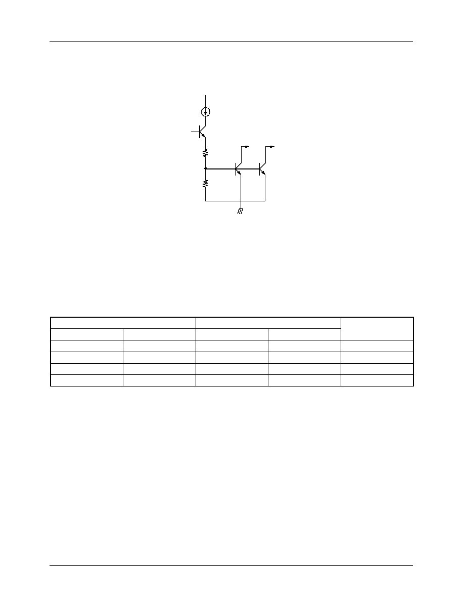
3. Logic Switch Circuit
This circuit define reference voltage of output.
When pin #4 is "H" and pin #5 is "L",
- V1 = Vzd + Vbe
Q4
+ Vbe
Q5
∑
=
∑
8.9V
- V2 = Vbeq 7 + Vsat
Q6
∑
=
∑
0.87V
V1 and V2 are related with the output voltage of the motor and change according to the voltage of pin #3 (V
CTL
).
4. Drive Output Circuit
V
1
= 8.9V
V
2
= 0.87V
V
O1
= V
1
- V
BEQ1
- V
BEQ2
V
O2
= V
Q6SAT
V
O
= V
O1
- V
O2
= V
1
- V
BEQ1
- V
BEQ2
- V
Q6SAT
I
RL
= (V
O1
- V
O2
) / R
L
4
5
3
SV
CC
V1
V2
Q4
Q5
Q6
Q7
V
CTL
7.4V
ZD
*
ZD : External Component
M
P
VCC
V1
R1
Q1
Q4
V2
V
O1
R2
V
O2
Q3
Q6
Q2
Q5
R
L
BI-DIRECTIONAL DC MOTOR DRIVER
8
Typical Perfomance Chracteristics
1.
1.
1.
1. V
V
V
V
CC
CC
CC
CC
vs
vs
vs
vs IIII
CC
CC
CC
CC
2.
2.
2.
2. Temperature
Temperature
Temperature
Temperature vs
vs
vs
vs IIII
CC
CC
CC
CC
3.
3.
3.
3. V
V
V
V
CTL
CTL
CTL
CTL
vs. Vo
vs. Vo
vs. Vo
vs. Vo
4.
4.
4.
4. Temperature vs. Vo
Temperature vs. Vo
Temperature vs. Vo
Temperature vs. Vo
CHARACTERISTIC GRAPHS
CHARACTERISTIC GRAPHS
CHARACTERISTIC GRAPHS
CHARACTERISTIC GRAPHS
0
1
2
3
4
5
6
7
8
9
10
0
2
4
6
8
10
12
14
16
18
20
V
CC
(V)
I
CC
(m
A
)
V
IN
= 0V
0
1
2
3
4
5
6
7
8
9
10
-35
-15
5
25
45
65
85
Temp.(
∞
C)
I
CC
(m
A
)
V
CC
= 12V
V
IN
= 0V
0
2
4
6
8
10
12
0
2
4
6
8
10
12
V
CTL
(V)
V
O
(V
)
V
CC
= 12V
V
IN
= 5V/0V
R
L
= 60
6.5
6.6
6.7
6.8
6.9
7.0
7.1
7.2
7.3
7.4
7.5
7.6
7.7
-35
-15
5
25
45
65
85
Temp.(
∞
C)
V
O
(V
)
V
CC
= 12V
V
CTL
= 7.4V
V
IN
= 5V/0V
R
L
= 60
5.
5.
5.
5. IIII
O
O
O
O
vs. V
vs. V
vs. V
vs. V
SAT
SAT
SAT
SAT
(UPPER)
(UPPER)
(UPPER)
(UPPER)
5.
5.
5.
5. IIII
O
O
O
O
vs. V
vs. V
vs. V
vs. V
SAT
SAT
SAT
SAT
(LOWER)
(LOWER)
(LOWER)
(LOWER)
0.0
0.5
1.0
1.5
2.0
2.5
3.0
0.2
0.4
0.6
0.8
1.0
1.2
I
O
(A)
V
SA
T
(V
)
V
CC
= 12V
V
CTL
= ope
V
IN
= 5V/0V
0.0
0.1
0.2
0.3
0.4
0.5
0.6
0.7
0.8
0.9
1.0
0.2
0.4
0.6
0.8
1.0
1.2
I
O
(A)
V
SA
T
(V
)
V
CC
= 12V
V
CTL
= open
V
IN
= 5V/0V
1.
1.
1.
1. V
V
V
V
CC
CC
CC
CC
vs
vs
vs
vs IIII
CC
CC
CC
CC
2.
2.
2.
2. Temperature
Temperature
Temperature
Temperature vs
vs
vs
vs IIII
CC
CC
CC
CC
3.
3.
3.
3. V
V
V
V
CTL
CTL
CTL
CTL
vs. Vo
vs. Vo
vs. Vo
vs. Vo
4.
4.
4.
4. Temperature vs. Vo
Temperature vs. Vo
Temperature vs. Vo
Temperature vs. Vo
CHARACTERISTIC GRAPHS
CHARACTERISTIC GRAPHS
CHARACTERISTIC GRAPHS
CHARACTERISTIC GRAPHS
0
1
2
3
4
5
6
7
8
9
10
0
2
4
6
8
10
12
14
16
18
20
V
CC
(V)
I
CC
(m
A
)
V
IN
= 0V
0
1
2
3
4
5
6
7
8
9
10
-35
-15
5
25
45
65
85
Temp.(
∞
C)
I
CC
(m
A
)
V
CC
= 12V
V
IN
= 0V
0
2
4
6
8
10
12
0
2
4
6
8
10
12
V
CTL
(V)
V
O
(V
)
V
CC
= 12V
V
IN
= 5V/0V
R
L
= 60
6.5
6.6
6.7
6.8
6.9
7.0
7.1
7.2
7.3
7.4
7.5
7.6
7.7
-35
-15
5
25
45
65
85
Temp.(
∞
C)
V
O
(V
)
V
CC
= 12V
V
CTL
= 7.4V
V
IN
= 5V/0V
R
L
= 60
5.
5.
5.
5. IIII
O
O
O
O
vs. V
vs. V
vs. V
vs. V
SAT
SAT
SAT
SAT
(UPPER)
(UPPER)
(UPPER)
(UPPER)
5.
5.
5.
5. IIII
O
O
O
O
vs. V
vs. V
vs. V
vs. V
SAT
SAT
SAT
SAT
(LOWER)
(LOWER)
(LOWER)
(LOWER)
0.0
0.5
1.0
1.5
2.0
2.5
3.0
0.2
0.4
0.6
0.8
1.0
1.2
I
O
(A)
V
SA
T
(V
)
V
CC
= 12V
V
CTL
= ope
V
IN
= 5V/0V
0.0
0.1
0.2
0.3
0.4
0.5
0.6
0.7
0.8
0.9
1.0
0.2
0.4
0.6
0.8
1.0
1.2
I
O
(A)
V
SA
T
(V
)
V
CC
= 12V
V
CTL
= open
V
IN
= 5V/0V
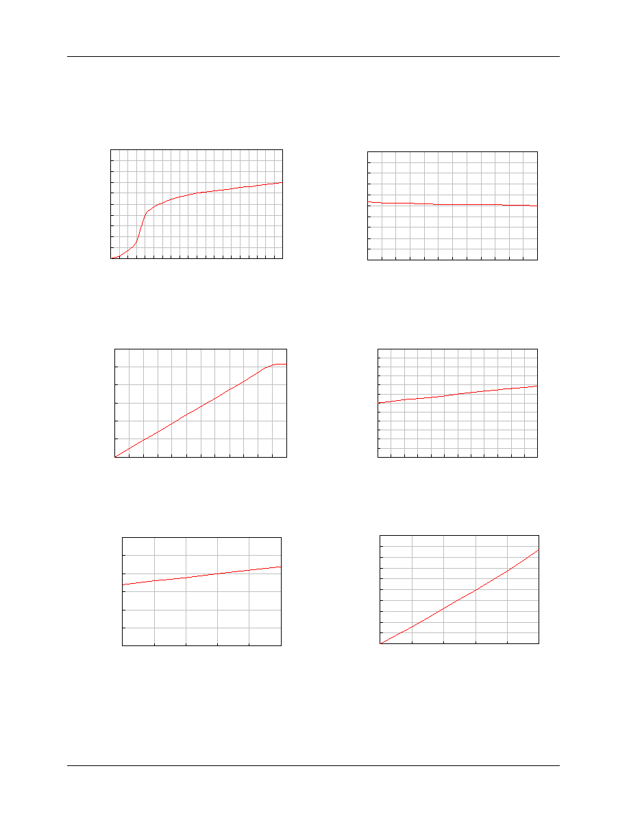
Figure 1. V
CC
vs I
CC
Figure 2. Temperature vs I
CC
Figure 3. V
CTL
vs V
O
Figure 4. Temperature vs V
O
Figure 5. I
O
vs V
SAT
(UPPER)
Figure 6. I
O
vs V
SAT
(LOWER)

BI-DIRECTIONAL DC MOTOR DRIVER
9
Test Circuits
A
A
V
CC
S1
S2
Z
D
7.4V
V
IN
S5
S4
1
2
5
6
7
8
GND
V
O1
V
CTL
V
IN1
V
IN2
SV
CC
PV
CC
V
O2
3
4
S3
A
A
FAN8082D

BI-DIRECTIONAL DC MOTOR DRIVER
10
Application Circuits
V
CC
Z
D
1
2
5
6
7
8
GND
V
O1
V
CTL
V
IN1
V
IN2
SV
CC
PV
CC
V
O2
3
4
104
104
FAN8082D
M
RS
*
Must use RS.

BI-DIRECTIONAL DC MOTOR DRIVER
11

BI-DIRECTIONAL DC MOTOR DRIVER
10/25/01 0.0m 001
Stock#DSxxxxxxxx
2001 Fairchild Semiconductor Corporation
LIFE SUPPORT POLICY
FAIRCHILD'S PRODUCTS ARE NOT AUTHORIZED FOR USE AS CRITICAL COMPONENTS IN LIFE SUPPORT DEVICES
OR SYSTEMS WITHOUT THE EXPRESS WRITTEN APPROVAL OF THE PRESIDENT OF FAIRCHILD SEMICONDUCTOR
CORPORATION. As used herein:
1. Life support devices or systems are devices or systems
which, (a) are intended for surgical implant into the body,
or (b) support or sustain life, and (c) whose failure to
perform when properly used in accordance with
instructions for use provided in the labeling, can be
reasonably expected to result in a significant injury of the
user.
2. A critical component in any component of a life support
device or system whose failure to perform can be
reasonably expected to cause the failure of the life support
device or system, or to affect its safety or effectiveness.
www.fairchildsemi.com
DISCLAIMER
FAIRCHILD SEMICONDUCTOR RESERVES THE RIGHT TO MAKE CHANGES WITHOUT FURTHER NOTICE TO ANY
PRODUCTS HEREIN TO IMPROVE RELIABILITY, FUNCTION OR DESIGN. FAIRCHILD DOES NOT ASSUME ANY
LIABILITY ARISING OUT OF THE APPLICATION OR USE OF ANY PRODUCT OR CIRCUIT DESCRIBED HEREIN; NEITHER
DOES IT CONVEY ANY LICENSE UNDER ITS PATENT RIGHTS, NOR THE RIGHTS OF OTHERS.