 | –≠–ª–µ–∫—Ç—Ä–æ–Ω–Ω—ã–π –∫–æ–º–ø–æ–Ω–µ–Ω—Ç: FAN8100N | –°–∫–∞—á–∞—Ç—å:  PDF PDF  ZIP ZIP |

©2005 Fairchild Semiconductor Corporation
www.fairchildsemi.com
Rev. 1.0.0
Features
∑ Two channel H-bridge drivers with built-in NPN and
vertical-PNP power transistors
∑ Four functions for each channel - Forward/Reserve/Stop/
Brake functions
∑ Special output pin for an RC car application - for a Turbo
function for Ch.A (five-function RF receiver chip RX-2
interface)
∑ Low stand-by current (typ. 0.1uA)
∑ Wide supply voltage range (PVCC=1.8V ~ 9.0V) suitable
for battery operated applications
∑ 3.3V and 5V micro-controller interface
∑ Low output saturation voltage (upper and lower total : typ.
0.15V@ 0.2A)
∑ High current outputs (max. 1.5A/Ch.)
∑ Parallel connection (Max Current : 3A)
∑ High thermal capability for high continuous output
currents
∑ Built-in spark killing diodes
∑ Built-in a thermal shutdown(TSD) function with
hysteresis
∑ Short circuit protected
∑ Temperature independent internal voltage reference
Description
The FAN8100N/FAN8100MTC is a monolithic two channel
dc motor drive IC designed for low voltage operated sys-
tems. It has dual H-bridge drivers, using NPN and vertical-
PNP power transistors with a low saturation voltage. Power
packages with heat sinks endure high continuous output cur-
rent. The high current and low saturation voltage feature
make this device suitable for dc motor applications such as
toy cars. It has also a built-in thermal shutdown protection
circuit with hysteresis.
12-DIPH-300
14-TSSOP
1
1
1
Typical Application
∑ General purpose dc motor driver
∑ Electronic toys - robots, RC cars
∑ Digital still camera(DSC) and film camera
∑ Home appliances and office equipment
∑ Precision instruments
Ordering Information
Device
Package
Operating Temp.
FAN8100N
12-DIPH-300
-
20 ~ +75
∞
C
FAN8100MTC
14-TSSOP
-
20 ~ +75
∞
C
FAN8100MTCX
14-TSSOP
-
20 ~ +75
∞
C
FAN8100N/FAN8100MTC
Low Voltage/Low Saturation 2-CH DC Motor Driver

FAN8100N/FAN8100MTC
2
Pin Assignments
Pin Definitions
Note: ( ) FAN8100MTC
Pin Number
Pin Name
I/O
Pin Function Description
1(12)
REVERSEB
I
Reverse logic input for channel B
2(13)
FORWARDB
I
Forward logic input for channel B
3(14)
OUT2B
O
Output2 of channel B
FIN(1)
GND
-
Ground
4(2)
OUT1B
O
Output1 of channel B
5(3)
PVCCB
-
Supply voltage for channel B output
6(4)
VCC
-
Logic and control circuit supply voltage
7(5)
D1A
O
Cathode of OUT1A upper diode
8(6)
PVCCA
-
Supply voltage for channel A output
9(7)
OUT1A
O
Output1 of channel A
FIN(8)
GND
-
Ground
10(9)
OUT2A
I
Output2 of channel A
11(10)
FORWARDA
I
Forward logic input for channel A
12(11)
REVERSEA
I
Reverse logic input for channel A
1
2
3
5
6
7
14
13
12
10
9
8
FAN8100MTC
O
U
T1B
GN
D
PV
CC
B
VC
C
PV
CC
A
D1
A
OU
T1
A
FO
R
W
A
R
D
B
OU
T2
B
R
EVE
RS
EA
FO
R
W
A
R
D
A
OU
T2
A
R
EVE
RS
EB
GN
D
11
4
1
2
3
FIN
4
5
6
12
11
10
FIN
9
8
7
FAN8100N
F
O
R
W
A
RDB
RE
VE
R
S
E
B
OU
T2
B
GN
D
PV
CCB
OU
T1
B
VCC
FO
R
W
A
R
D
A
RE
V
E
R
S
E
A
GND
OUT
1
A
PVC
CA
OUT
2
A
D1
A

FAN8100N/FAN8100MTC
3
Internal Block Diagram
Note: FAN8100N pin number
9
3
8
5
7
4
Ch. A
Control
Circuit
Ch. B
Control
Circuit
Bias & TSD
Circuit
11
2
12
10
1
6
Fin
PVCCA
OUT1A
OUT2A
D1A
PVCCB
OUT1B
OUT2B
VCC
GND
FORWARDA
REVERSEA
FORWARDB
REVERSEB
FAN8100N/FAN8100MTC
4
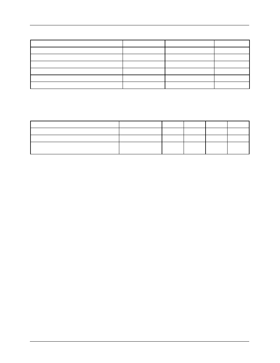
Absolute Maximum Ratings (Ta = 25
∞
C)
Note: ( ) FAN8100MTC
Recommended Operating Conditions
(Ta = 25
∞
C)
Note: See the characteristics graphs.
Parameter
Symbol
Value
Unit
Maximum logic and control supply voltage
VCC
(MAX)
10.5
V
Maximum output supply voltage
PVCC
(MAX)
10.5
V
Maximum output applied voltage
VOUT
(MAX)
PVCC + VD
V
Maximum applied input voltage
VIN
(MAX)
10.0
V
Maximum D1A Voltage
VD1A
(MAX)
PVCCA + 4.5
V
Peak output current per channel
IOUT
(PEAK)
1.5(1.2)
A
Parameter
Symbol
Min.
Typ.
Max
Unit
Logic and control circuit supply voltage
VCC
2.2
-
9.0
V
Output supply voltage
PVCC
1.8
-
9.0
V
D1A Voltage
VD1A
PVCCA
-
PVCCA
+3.0
V

FAN8100N/FAN8100MTC
5
Typical Thermal Characteristics
Notes:
1. When mounted on JEDEC 76.2mm
◊
114mm
◊
1.57mm PCB (FR-4 glass epoxy material).
2. On the junction. These values are design specifications.
Power Dissipation Curve
Notes:
1. When mounted on JEDEC 76.2mm
◊
114mm
◊
1.57mm PCB (FR-4 glass epoxy material).
2. Power dissipation reduces 16mW/
∞
C
(FAN8100N)
and
32mW/
∞
C
(FAN8100MTC)
for using above Ta=25
∞
C
.
3. Do not exceed PD and SOA(Safe Operating Area).
Parameter
Symbol
Value
Unit
Power dissipation
PD
note1
FAN8100N:
2
.0
FAN8100MTC
:
1.0
W
Operating temperature
TA
-
20 ~ 75
∞
C
Storage temperature
TSTG
-
40 ~ 125
∞
C
Junction temperature
TJ
150
∞
C
Thermal shutdown temperature
TSD
note2
150
∞
C
Thermal shutdown hysteresis temperature
TSD
note2
50
∞
C
0
0
25
50
75
100
125
Ambient temperature, Ta [
∞
C]
150
175
1.0
2.0
Power
Dissipation
: PD[W]
SOA
FAN8100N
0
0
25
50
75
100
125
Ambient temperature, Ta [
∞
C]
150
175
0.5
1
.0
Power
Dissipation
: PD[W]
SOA
FAN8100MTC

FAN8100N/FAN8100MTC
6
Electrical Characteristics
(Ta=25
∞
C, VCC=3V, PVCCA=PVCCB=3V, unless otherwise specified)
Note: ( ) FAN8100MTC
Timing Characteristics
(Ta=25
∞
C, VCC=3V, PVCCA=PVCCB=3V, unless otherwise specified)
Note: with 1nF Capacitor Loads
Parameter
Symbol
Conditions
Min.
Typ.
Max.
Unit
Stand-by current
(I
VCC
+I
PVCCA
+I
PVCCB
)
ICC0
All input pins=0V,
with output pins open
-
0.1
10
uA
VCC supply current 1 (I
VCC
)
ICC1
Forward or Reverse
(single channel)
-
4
6
mA
VCC supply current 2 (I
VCC
)
ICC2
Brake (single channel)
-
5.5
8
mA
Total supply current 1
(I
VCC
+I
PVCCA
+I
PVCCB
)
ICC3
Forward or Reverse
(single channel)
with output pins open
-
30(20) 40(27)
mA
Total supply current 2
(I
VCC
+I
PVCCA
+I
PVCCB
)
ICC4
Brake (single channel)
with output pins open
-
55(35) 65(45)
mA
Saturation voltage 1
(upper + lower output transistors total)
VSAT1
FORWARDA=3V, other
input pins=0V,
IOUT=0.2A
-
0.15
0.25
V
Saturation voltage 2
(upper + lower output transistors total)
VSAT2
FORWARDA=3V, other
input pins=0V,
IOUT=0.4A
-
0.35
0.55
V
Input high level voltage
VINH
-
1.8
-
VCC
V
Input low level voltage
VINL
-
-
0.3
-
0.7
V
Input current
IIN
VIN=3V,
per each input pin
-
100
200
uA
Spark-killing diode leakage current
ILEAK
VCC=9V, PVCC=9V
-
-
30
uA
Spark-killing diode voltage drop
VD
IOUT=0.4A
-
-
1.7
V
Parameter
Symbol
Conditions
Min.
Typ.
Max.
Unit
Output rising time
tR
input rising time = 20ns
output voltage 10% to 90%
-
0.3
-
us
Output falling time
tF
input falling time = 20ns
output voltage 90% to 10%
-
0.3
-
us
Input to output propagation delay
tPLH
input rising time = 20ns
input 50% to output 50%
-
1
-
us
tPHL
input falling time = 20ns
input 50% to output 50%
-
1
-
us

FAN8100N/FAN8100MTC
7
Function Descriptions
Logical Truth Table
Channel A
Channel B
Z: high-impedance
Time Domain Waveforms
Notes: **See typical application circuits.
FORWARDA
REVERSEA
OUT1A
OUT2A
Function
L
L
Z
Z
Stand-by (Stop)
H
L
H
L
Forward
L
H
L
H
Reverse
H
H
L
L
Brake
FORWARDB
REVERSEB
OUT1B
OUT2B
Function
L
L
Z
Z
Stand-by (Stop)
H
L
H
L
Forward
L
H
L
H
Reverse
H
H
L
L
Brake
H
L
H
H
L
H
H
L
L
FORWARD
REV ERSE
TURBO*
(V
- V
)
OUT1
OUT 2
Output Voltage
0
PV CC
-PV CC
V S
Input
Signals
*Only for channel A
: High impedance
time
**Should be 'L'
**Should be 'L'
**when an external turbo circuit is used

FAN8100N/FAN8100MTC
8
Application Information
1. Thermal Shutdown (TSD)
Thermal Shutdown Circuit turns OFF all outputs when the junction temperature typically reaches 150
∞
C
. It is intended to pro-
tect the device from failures due to excessive junction temperature.
The Thermal Shutdown has the hysteresis of 40
∞
C
approximately
.
2. Printed Circuit Board (PCB) Layout
If high current flows on the power supply(PVCC) and GND line, it can be misoperated due to the line oscillation.
The following points should be kept in mind regarding as the pattern layout to prevent it.
∑ Making the wiring lines thick and short, especially between power supply (PVCC) and GND.
∑ Putting a passthrough capacitor near the IC
The R
th-ja
of the FAN8100N/MTC can be reduced by soldering the GND pins to a suitable copper area of the printed circuit
board as shown in following figure. It is recommended the copper area is as large as possible.
Example of PCB copper area which is used as heatsink

FAN8100N/FAN8100MTC
9
Typical Application Circuits
1. RF Remote Controlled Car
2. RF Remote Controlled Car with a Turbo Function
1
2
3
FIN
4
5
6
12
11
10
FIN
9
8
7
FAN8100N/FAN8100MTC
FO
R
W
A
R
D
B
R
EVE
R
SEB
VC
C
GN
D
OU
T
1
B
OU
T
2
B
PVC
C
B
F
O
RW
A
R
DA
R
EVER
SEA
GN
D
OU
T1A
D1
A
OU
T2A
PVC
C
A
1
2
3
6
4
7
5
8
16
15
13
11
14
12
10
9
GN
D
VO
2
SI
OS
C
I
OS
C
O
LE
F
T
W
A
RD
RI
G
H
T
W
A
R
D
NC
VO
1
VI2
VD
D
TU
R
B
O
FOR
W
A
R
D
B
A
C
KW
AR
D
VI1
NC
RF Signal
RF Circuits
(Discrete Parts)
BACKWARD
FORWARD
LEFT
RIGHT
Receiver Controller
RX-2
1
2
3
FIN
4
5
6
12
11
10
FIN
9
8
7
FAN8100N/FAN8100MTC
FOR
W
A
R
D
B
RE
V
E
R
S
E
B
VC
C
GN
D
OU
T
1
B
OU
T
2
B
PV
C
C
B
FOR
W
A
R
D
A
RE
V
E
R
S
E
A
GN
D
OU
T1
A
D1A
OU
T2
A
PV
C
C
A
1
2
3
6
4
7
5
8
16
15
13
11
14
12
10
9
GN
D
VO
2
SI
OS
C
I
OS
C
O
LE
F
T
W
A
RD
RIG
H
T
W
A
R
D
NC
VO
1
VI
2
VD
D
TU
R
B
O
FOR
W
A
R
D
B
A
CK
W
A
RD
VI
1
NC
RF Signal
RF Circuits
(Discrete Parts)
BACKWARD
FORWARD
LEFT
RIGHT
Receiver Controller
RX-2
Q1
R2
R1
Q2
Q3
FAN8100N/FAN8100MTC
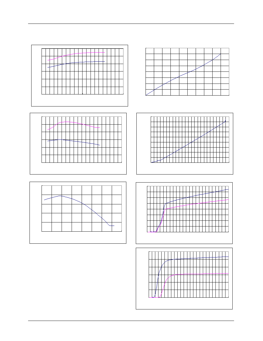
10
Typical Performance Characteristics (FAN8100N)
0
10
20
30
40
50
60
-50
0
50
100
150
Ambient Temperature Ta []
P
V
CC
Cu
rr
e
n
t D
r
ai
n
IP
V
C
C
[
mA
VCC = PVCC = 3V
Brake
Forward / Reverse
38
39
40
41
42
43
-40
-20
0
20
40
60
80
100
120
Ambient Temperature Ta []
In
p
u
t
C
u
r
r
e
n
t
II
N
[
uA
]
VCC = PVCC = VIN = 3V
0
0.1
0.2
0.3
0.4
0.5
0.6
0.7
0.8
0
0.1
0.2
0.3
0.4
0.5
0.6
0.7
0.8
0.9
1
Output Current IO []
O
u
tp
u
t
S
a
tu
r
a
ti
o
n
V
o
l
t
a
g
e
[
V
]
0
20
40
60
80
100
120
140
160
180
0
2
4
6
8
10
Input Voltage VIN [V]
I
n
p
u
t C
u
r
r
e
n
t I
I
N
[
uA
]
VCC = PVCC = 9V
0
1
2
3
4
5
6
7
8
0
2
4
6
8
10
Supply Voltage VCC [V]
Su
p
p
l
y
Cu
r
r
e
n
t ICC
[
mA
]
VCC = PVCC = 3V
Brake
Forward / Reverse
0
10
20
30
40
50
60
0
2
4
6
8
10
Supply Voltage PVCC [V]
Su
p
p
l
y
Cu
rr
e
n
t IP
V
CC
[
mA
]
VCC = PVCC = 3V
Brake
Forward / Reverse
0
1
2
3
4
5
6
-50
0
50
100
150
Ambient Temperature Ta []
V
C
C Cu
rr
e
n
t
D
r
a
i
n
I
C
C
[
mA
]
VCC = PVCC = 3V
Brake
Forward / Reverse

FAN8100N/FAN8100MTC
11
Typical Performance Characteristics
(Continued)
(FAN8100MTC)
0
1
2
3
4
5
6
-50
0
50
100
150
Ambient Temperature Ta []
V
C
C C
u
r
r
e
n
t
Dr
ai
n
IC
C
[
mA
VCC = PVCC = 3V
Brake
Forward / Reverse
0
5
10
15
20
25
30
35
-50
0
50
100
150
Ambient Temperature Ta []
P
V
CC Cu
r
r
e
n
t
Dr
ai
n
IPV
CC
[
mA
VCC = PVCC = 3V
Brake
Forward / Reverse
37
38
39
40
41
42
43
-40
-20
0
20
40
60
80
100
120
Ambient Temperature Ta []
I
n
p
u
t C
u
r
r
e
n
t I
I
N
[
uA
]
VCC = PVCC = VIN = 3V
0
0.2
0.4
0.6
0.8
1
1.2
0
0.1
0.2
0.3
0.4
0.5
0.6
0.7
0.8
0.9
1
Output Current IO []
O
u
t
p
u
t
Sa
t
u
ra
t
i
o
n
V
o
l
t
a
g
e
[
V
]
0
20
40
60
80
100
120
140
160
180
0
2
4
6
8
10
Input Voltage VIN [V]
I
n
p
u
t
Cu
rre
n
t
II
N
[
uA
]
VCC = PVCC = 9V
0
1
2
3
4
5
6
7
8
0
2
4
6
8
10
Supply Voltage VCC [V]
Su
p
p
l
y
C
u
r
r
e
n
t ICC
[
mA
]
VCC = PVCC = 3V
Brake
Forward / Reverse
0
5
10
15
20
25
30
35
0
2
4
6
8
10
Supply Voltage PVCC [V]
S
u
ppl
y
C
u
r
r
e
n
t
I
P
V
C
C
[
mA
]
VCC = PVCC = 3V
Brake
Forward / Reverse

FAN8100N/FAN8100MTC
12
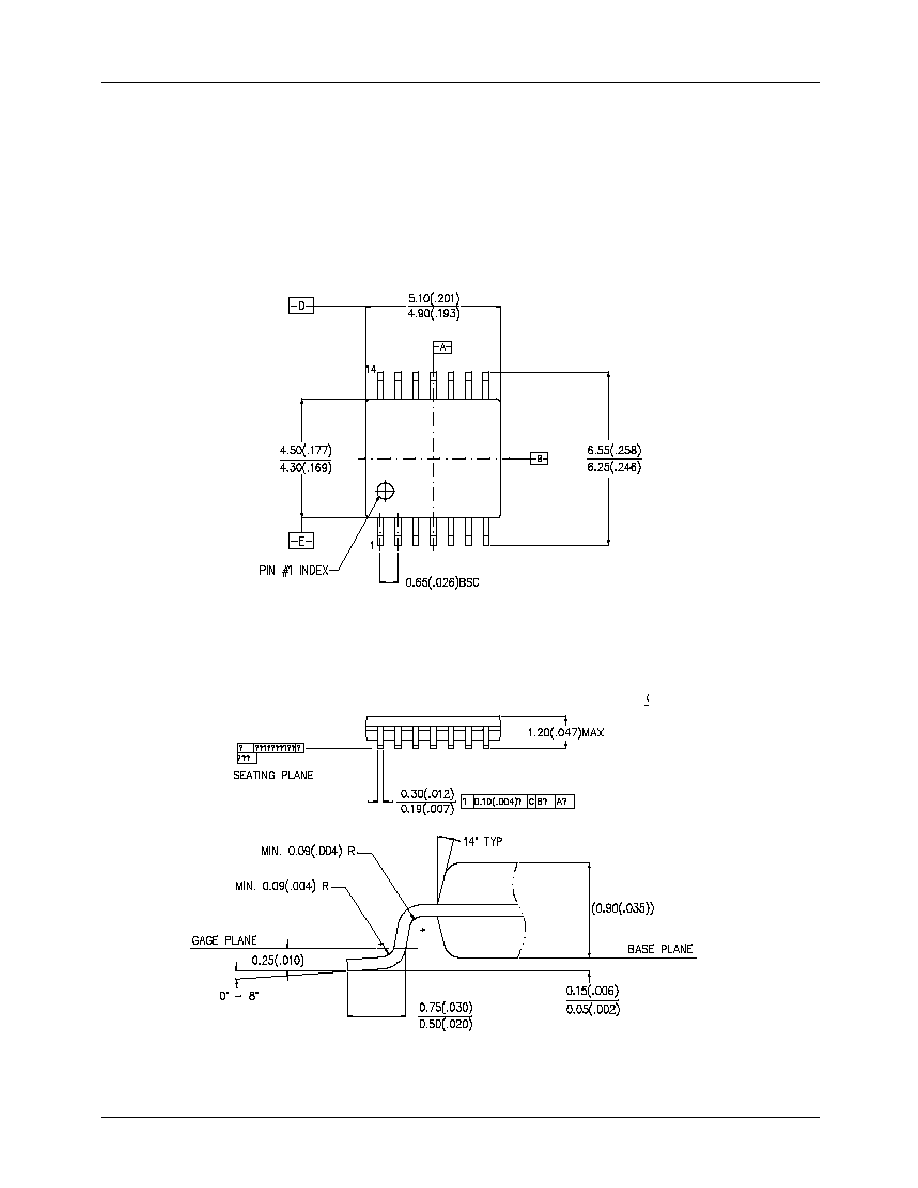
Mechanical Dimensions (Unit: mm)
Package Dimension
12-DIPH-300
FAN8100N/FAN8100MTC
13
Mechanical Dimensions (Unit: mm)
(Continued)
Package dimensions
14-TSSOP

FAN8100N/FAN8100MTC
6/9/05 0.0m 001
Stock#DSxxxxxxxx
2005 Fairchild Semiconductor Corporation
LIFE SUPPORT POLICY
FAIRCHILD'S PRODUCTS ARE NOT AUTHORIZED FOR USE AS CRITICAL COMPONENTS IN LIFE SUPPORT DEVICES
OR SYSTEMS WITHOUT THE EXPRESS WRITTEN APPROVAL OF THE PRESIDENT OF FAIRCHILD SEMICONDUCTOR
CORPORATION. As used herein:
1. Life support devices or systems are devices or systems
which, (a) are intended for surgical implant into the body,
or (b) support or sustain life, and (c) whose failure to
perform when properly used in accordance with
instructions for use provided in the labeling, can be
reasonably expected to result in a significant injury of the
user.
2. A critical component in any component of a life support
device or system whose failure to perform can be
reasonably expected to cause the failure of the life support
device or system, or to affect its safety or effectiveness.
www.fairchildsemi.com
DISCLAIMER
FAIRCHILD SEMICONDUCTOR RESERVES THE RIGHT TO MAKE CHANGES WITHOUT FURTHER NOTICE TO ANY
PRODUCTS HEREIN TO IMPROVE RELIABILITY, FUNCTION OR DESIGN. FAIRCHILD DOES NOT ASSUME ANY
LIABILITY ARISING OUT OF THE APPLICATION OR USE OF ANY PRODUCT OR CIRCUIT DESCRIBED HEREIN; NEITHER
DOES IT CONVEY ANY LICENSE UNDER ITS PATENT RIGHTS, NOR THE RIGHTS OF OTHERS.