©2001 Fairchild Semiconductor Corporation
www.fairchildsemi.com
Rev.1.0.1
Features
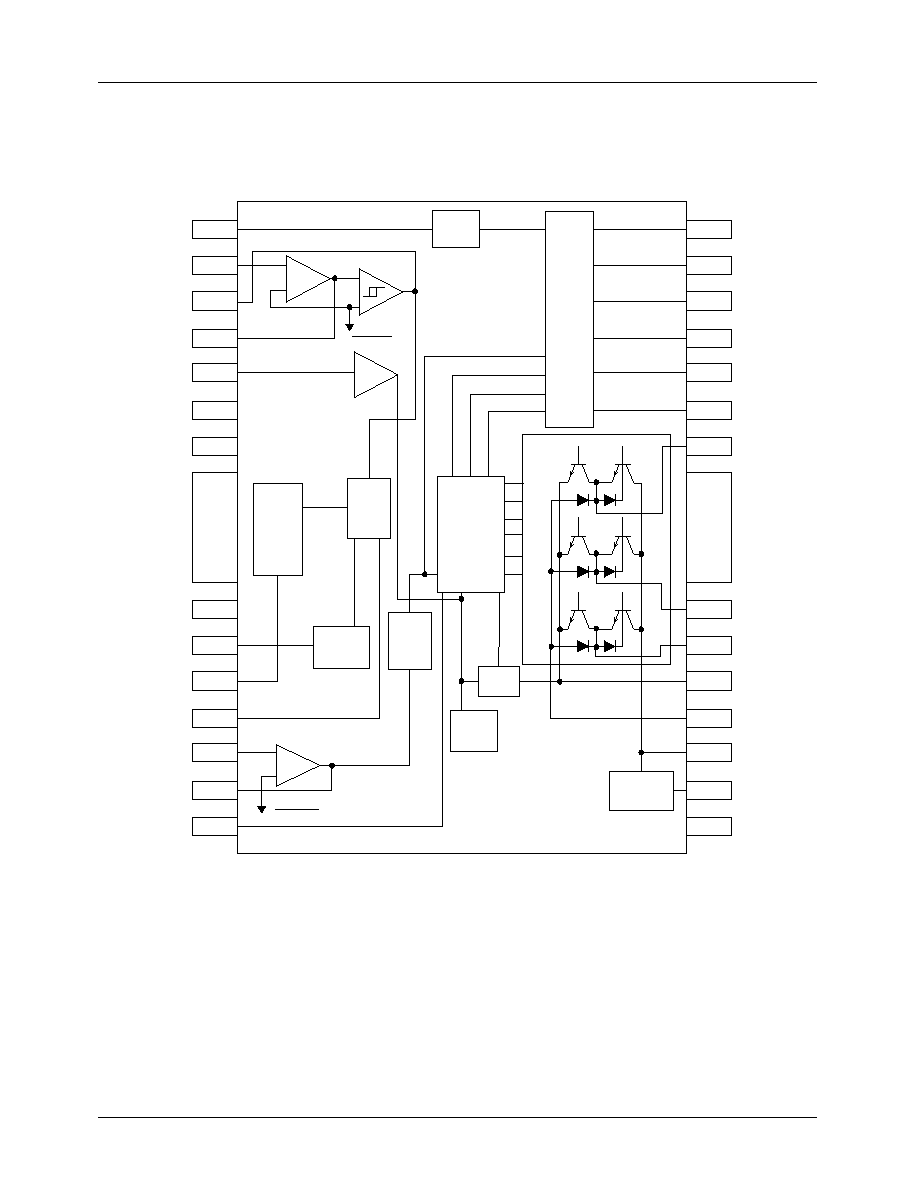
∑ 3-Phase BLDC motor driver IC with speed control
∑ Phase Locked Loop (PLL) speed control
∑ Built-in phase locked detector output
∑ Current linear drive scheme
∑ External clock for arbitrary motor speed
∑ Built-in FG amplifier and integrating amplifier
∑ Auto Gain Control (AGC) circuit for compensation hall
amplifier
∑ Built-in protection circuits (over-current limit, under
voltage limit, thermal shut down)
Description
The FAN8400D is a monolithic integrated circuit. it is one
driver for laser beam printer (LBP) polygon mirror motor,
which has single chip implementation of all circuits. For
extremely high rotational precision, it employs the phase
locked loop (PLL) speed control scheme.
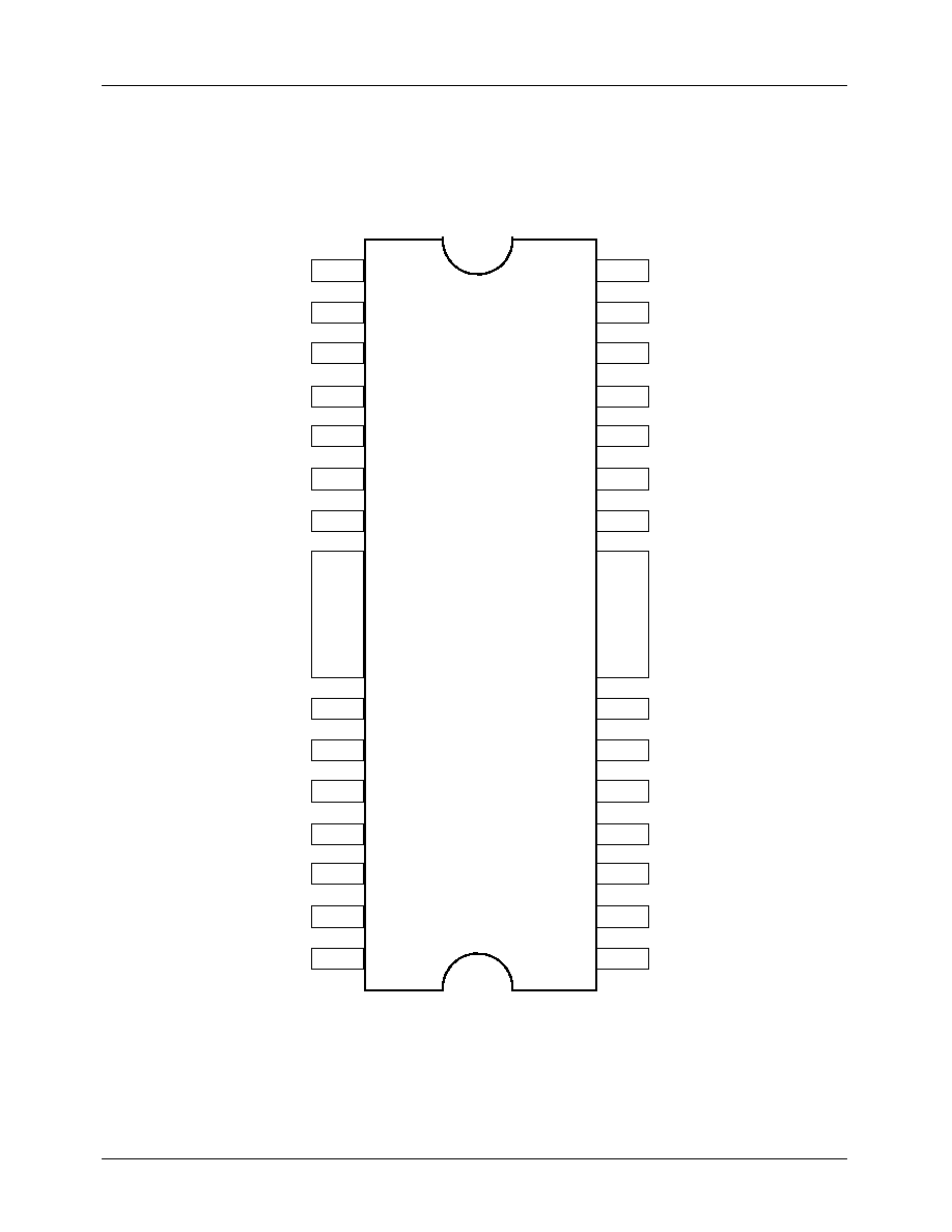
28-SSOPH-375SG2
Typical application
∑ Polygon mirror motor drive IC for laser beam printer
∑ Polygon mirror motor drive IC for facsimile
∑ Polygon mirror motor drive IC for duplicator
∑ Polygon mirror motor drive IC for multi function printer
∑ General 3 phase BLDC motor drive IC
Ordering Information
Device
Package
Operating Temp
FAN8400BD3
28-SSOPH-375SG2
-
20
∞
C ~ +80
∞
C
FAN8400BD3TF 28-SSOPH-375SG2
-
20
∞
C ~ +80
∞
C
FAN8400D (FAN8400BD3)
3-Phase BLDC Motor Driver with PLL

FAN8400D (FAN8400BD3)
3
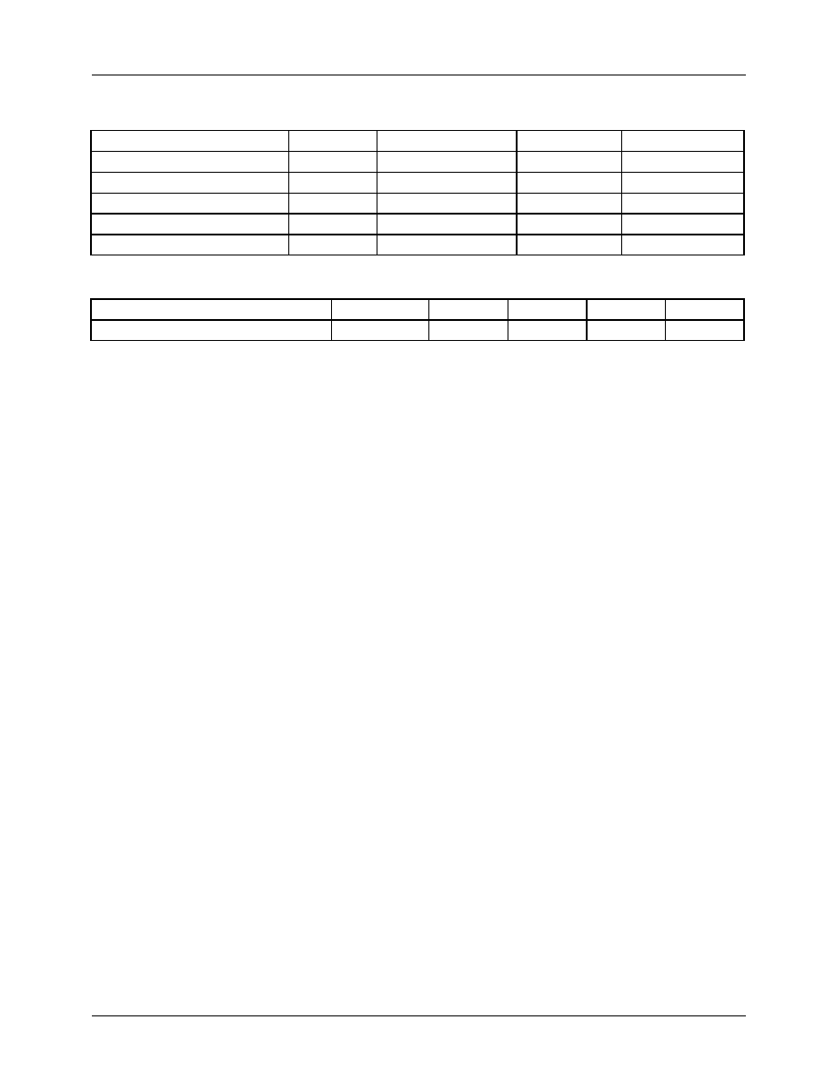
Pin Definitions
Pin Number
Pin Name
Pin Function Description
1
AGC
AGC amplifier frequency characteristics correction
2
FG
IN-
FG amplifier inverting input
3
FG
S
FG pulse output
4
FG
OUT
FG amplifier output
5
S/S
Stop and start
6
NC
-
7
NC
-
8
SGND
Signal ground
9
LD
Phase locked loop detector output
10
ECLK
External clock
11
PD
Phase locked loop detector output
12
E
I
Error amplifier inverting input
13
E
O
Error amplifier output
14
F
C
Control amplifier frequency correction
15
NC
-
16
V
REG
Regulator voltage stabilization output
17
V
CC
Power supply
18
PGND
Power ground
19
R
F
Output current detection
20
U
U output
21
V
V output
22
W
W output
23
H
V+
V hall amplifier non inverting input
24
H
V-
V hall amplifier inverting input
25
H
U+
U hall amplifier non inverting input
26
H
U-
U hall amplifier inverting input
27
H
W+
W hall amplifier non inverting input
28
H
W-
W hall amplifier inverting input