©2002 Fairchild Semiconductor Corporation
www.fairchildsemi.com
Rev.1.0.0
Features
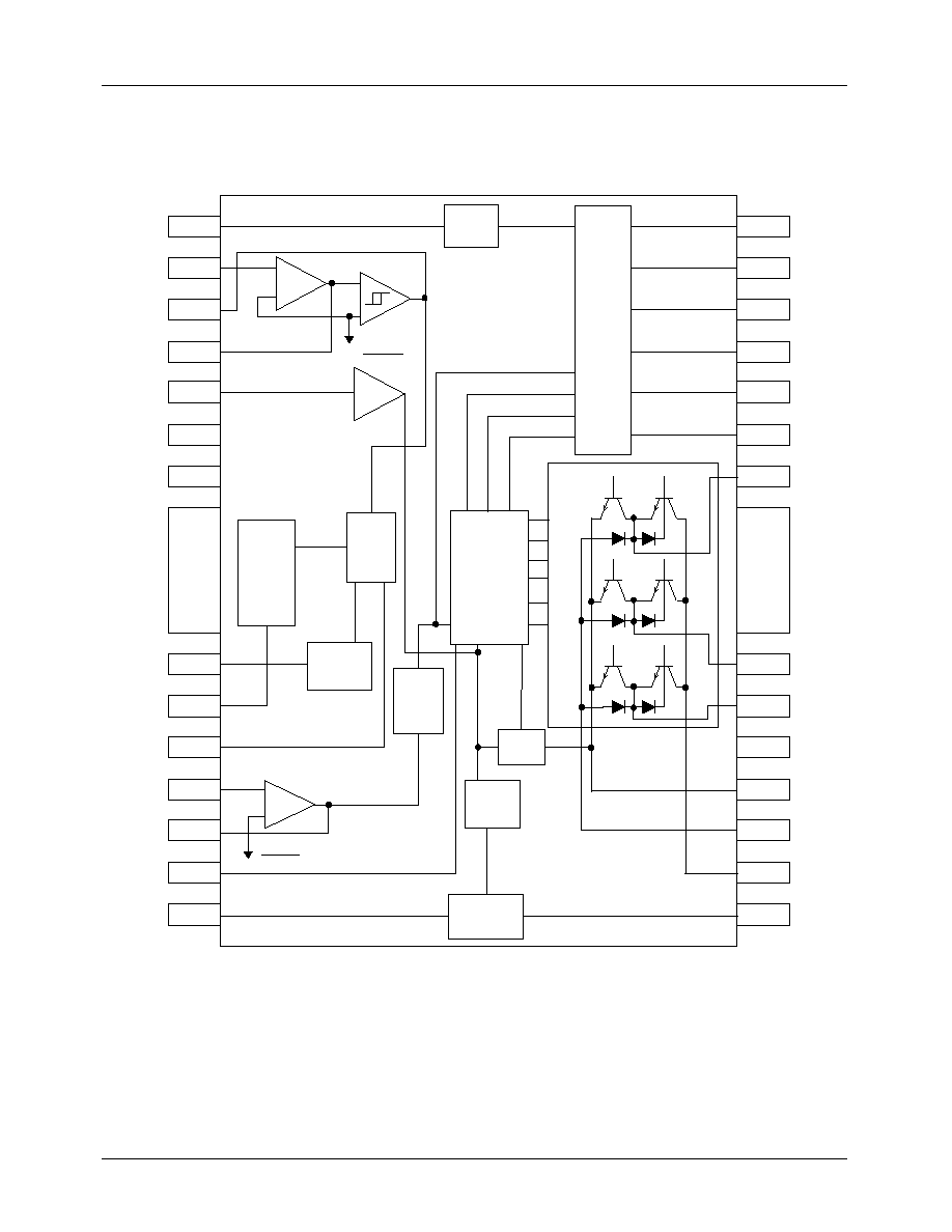
∑ 3-Phase BLDC motor drive IC with speed control
∑ Phase Locked Loop (PLL) speed control
∑ Built-in phase locked detector output
∑ External clock for control of motor speed
∑ Built-in FG amplifier and FG schmidt comparator
∑ Built-in integrating amplifier with phase error
∑ Auto Gain Control (AGC) circuit for compensation hall
amplifier
∑ Built-in protection circuits (over-current limit, under-
voltage limit, thermal shut down)
Description
The FAN8403D3 is a monolithic integrated circuit. It is suit-
able for polygon mirror motor of laser beam printer (LBP).
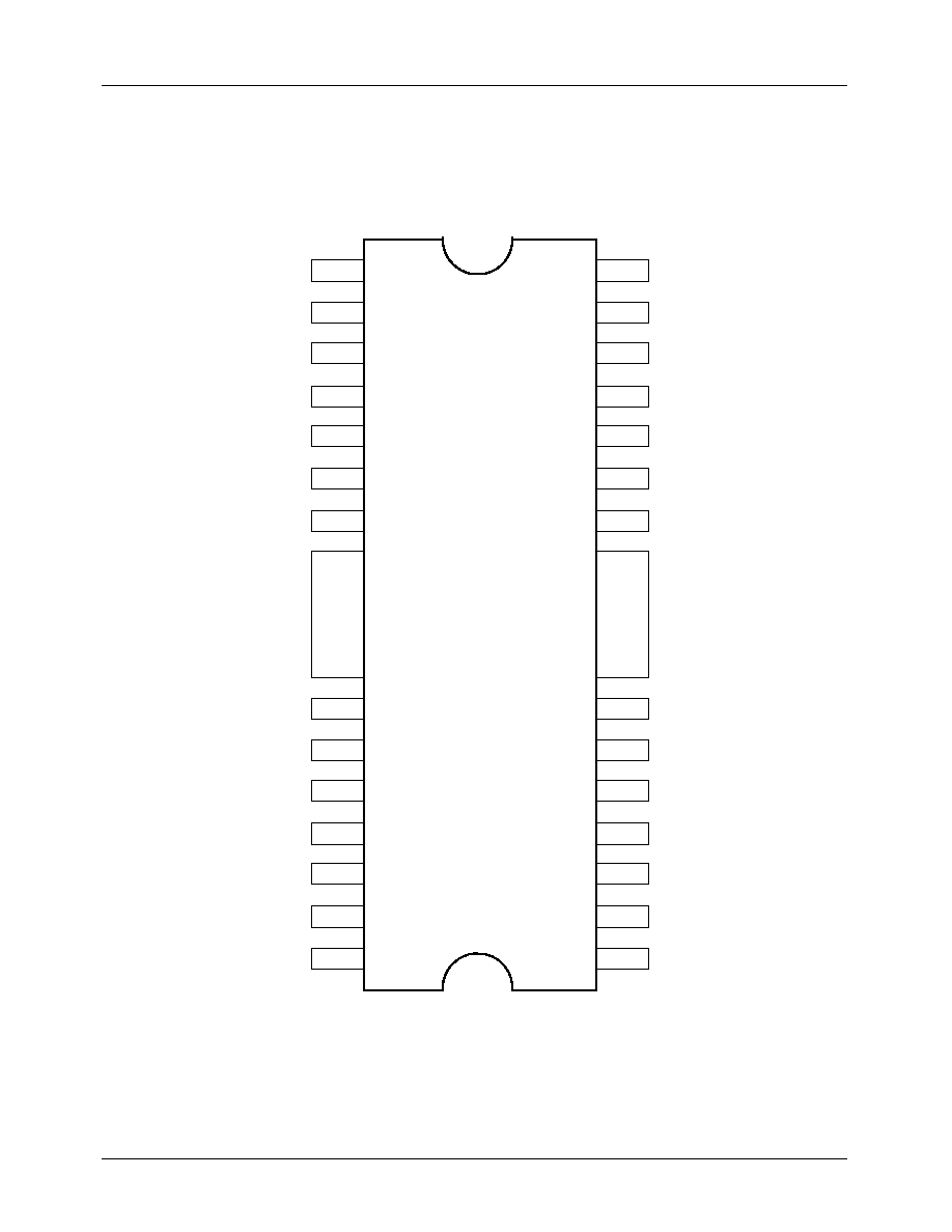
28-SSOPH-375SG2
Typical application
∑ Polygon mirror motor for laser beam printer
∑ Polygon mirror motor for facsimile
∑ Polygon mirror motor for duplicator
∑ Polygon mirror motor for multi-function printer
∑ General 3 phase BLDC motor
Ordering Information
Device
Package
Operating Temp.
FAN8403D3
28-SSOPH-375SG2
-
20
∞
C ~ +80
∞
C
FAN8403D3TF 28-SSOPH-375SG2
-
20
∞
C ~ +80
∞
C
FAN8403D3
3-Phase BLDC Motor Driver with PLL

FAN8403D3
3
Pin Definitions
Pin Number
Pin Name
Pin Function Description
1
AGC
AGC Amplifier Frequency Characteristics Correction
2
FG
IN-
FG Amplifier Inverting Input
3
FG
S
FG Pulse Output
4
FG
OUT
FG Amplifier Output (Open collect)
5
S/S
Stop And Start
6
NC
-
7
SGND
Signal Ground
8
LD
Phase Locked Loop Detector Output (Open Collect)
9
ECLK
External Clock
10
PD
Phase Locked Loop Detector Output
11
EI
Error Amplifier Inverting Input
12
EO
Error Amplifier Output
13
FC
Control Amplifier Frequency Correction
14
V
REG
Regulator Voltage Stabilization Output
15
SV
CC
Signal V
CC
16
PV
CC
Power V
CC
17
PGND
Power Ground
18
RF
Output Current Detection
19
NC
-
20
U
U Output
21
V
V Output
22
W
W Output
23
HV+
V Hall Amplifier Non Inverting Input
24
HV-
V Hall Amplifier Inverting Input
25
HU+
U Hall Amplifier Non Inverting Input
26
HU-
U Hall Amplifier Inverting Input
27
HW+
W Hall Amplifier Non Inverting Input
28
HW-
W Hall Amplifier Inverting Input
FAN8403D3
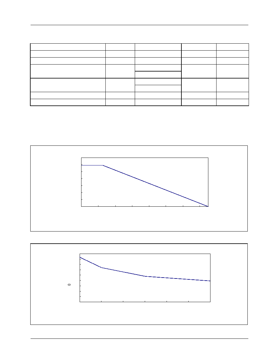
5
Absolute Maximum Ratings (Ta = 25
∞
∞
∞
∞
C)
Note 1.
PCB Condition: Thickness (1.6mm), Dimension (76.2mm * 114.3mm)
Refer: EIA/JSED 51-3 & EIA/JSED 51-7
Note 2. Air condition (0m/s)
Note 3. Air condition (3m/s)
Power Dissipation Curve (Air condition = 0m/s)
Air Speed &
JA
Parameter
Symbol
Value
Unit
Remark
Maximum Supply Voltage
V
CCMAX
30
V
-
Maximum Output Current
I
OMAX
1.0
A
-
Maximum Power Dissipation
note1
P
DMAX
3.0
note2
W
-
5.25
note3
Thermal Resistance
note1
JA
41.57
note2
∞
C/W
-
23.81
note3
Operating Temperature
T
OPR
-
20 ~ +80
∞
C
-
Storage Temperature
T
STG
-
50 ~ +150
∞
C
-
0
0.5
1
1.5
2
2.5
3
3.5
0
20
40
60
80
100
120
140
Tc or Ta[∞C]
Pd[W]
0
5
10
15
20
25
30
35
40
45
0
1
2
3
4
5
6
Air Speed[m/s]
JA[∞C/W]