 | –≠–ª–µ–∫—Ç—Ä–æ–Ω–Ω—ã–π –∫–æ–º–ø–æ–Ω–µ–Ω—Ç: FAN8434X | –°–∫–∞—á–∞—Ç—å:  PDF PDF  ZIP ZIP |
©2004Fairchild Semiconductor Corporation
www.fairchildsemi.com
Rev. 1.0.1
Features
Capstan motor drive block
∑ 3-phase, linear BLDC motor driver with 3 hall sensors.
∑ Built-in FG amplifier.
∑ Forward and reverse rotation function.
∑ Built-in amplitude limiter.
Drum motor drive block
∑ 3-phase soft commutating sensor less drive method.
∑ Built-in FG amplifier.
∑ Built-in PG amplifier.
Loading motor drive block
∑ Single phase H-bridge driving method.
∑ 4-mode selection function(forward, reverse,
brake,standby).
Common block
∑ Built-in TSD(thermal shut down)
∑ Built-in 4-normal op-amp.
Description
The FAN8434 is a camcorder one-chip motor driver IC. It is
composed of capstan motor driver , drum motor driver and
loading motor driver.
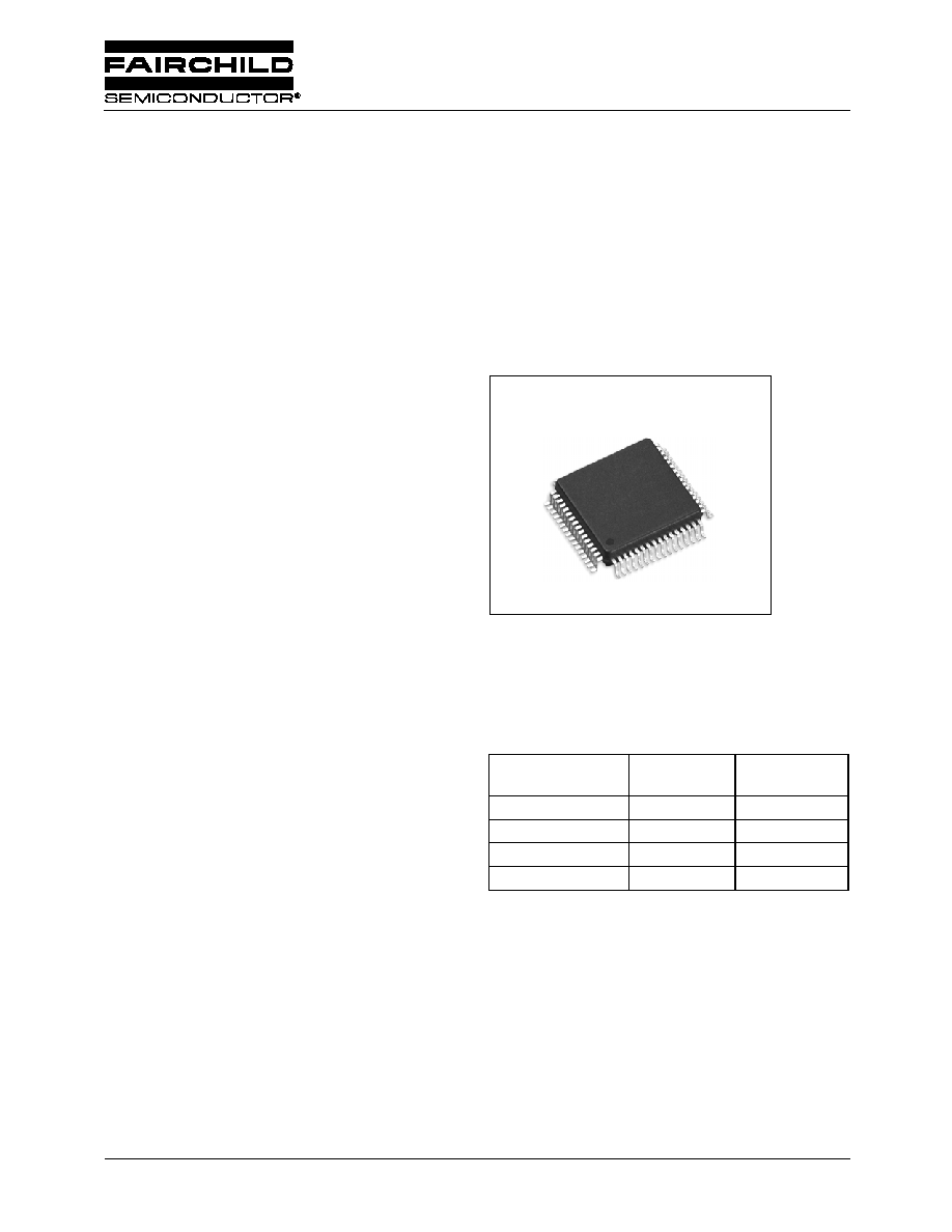
64-LQFP-1010
FAN8434
Camcorder 3 in 1 Motor Driver
Typical Applications
∑ Camcorder
Ordering Information
Notes:
1. X: Tape & Reel
2. NL: Lead-free type
Device
Package
Operating
Temp.
FAN8434
64-LQFP-1010
-25∞C ~ +75∞C
FAN8434_NL
note2
64-LQFP-1010
-25∞C ~ +75∞C
FAN8434X
note1
64-LQFP-1010
-25∞C ~ +75∞C
FAN8434X_NL
note2
64-LQFP-1010
-25∞C ~ +75∞C

FAN8434
2
Pin Assignments
12
11
10
9
8
7
6
5
4
3
2
1
16
15
14
13
28
27
26
25
24
23
22
21
20
19
18
17
32
31
30
29
37
38
39
40
41
42
43
44
45
46
47
48
33
34
35
36
53
54
55
56
57
58
59
60
61
62
63
64
49
50
51
52
FAN8434
D_FGIN
VREF
D_PGIN
D_PGC
D_PGOUT
GND
D_WIN
D_VIN
D_UIN
D_COM
VCC1
FC2
FILTER
FC1
OSC
D_FR
OP
I
N
3-
OP
OU
T
3
FWD
REV
L_
VM
OP
I
N
1-
OP
I
N
1+
OP
OU
T
1
OP
OU
T
2
OP
I
N
2+
OP
I
N
2-
SELC
S
L
P
CS
C1
CS
C2
OP
I
N
4-
OP
OU
T
4
HU-
HU+
C_WOUT
C_RS
C_VOUT
C_STBY
C_UOUT
D_WOUT
D_RS
D_VOUT
D_UOUT
D_VM
L_OUT2
L_RS
L_OUT1
L_ILIM
HV+
HV-
HW+
HW-
C_
VM
VH
+
VH
-
VC
C2
C_
F
R
AN
G
L
E
C_
F
G
I
N
+
C_
F
G
I
N
-
C_
F
G
O
U
T
D_
F
G
O
U
T
D_
S
T
B
Y
D_
F
G
I
N
1

FAN8434
3
Pin Definitions
Pine Number
Pin Name
I/O
Pin Function Description
1
OPIN3-
I
OP amp. 3 input -
2
OPOUT3
O
OP amp. 3 output
3
FWD
I
Loading motor forward input
4
REV
I
Loading motor reverse input
5
L_VM
-
Loading motor power supply voltage
6
OPIN1-
I
OP amp. 1 input -
7
OPIN1+
I
OP amp. 1 input +
8
OPOUT1
O
OP amp. 1 output
9
OPOUT2
O
OP amp. 2 output
10
OPIN2+
I
OP amp. 2 input +
11
OPIN2-
I
OP amp. 2 input -
12
SELCSLP
I
Selection pin for oscillator 's slant
13
CSC1
-
Drum motor soft commutating oscillation 1
14
CSC2
-
Drum motor soft commutating oscillation 2
15
OPIN4-
I
OP amp. 4 input -
16
OPOUT4
O
OP amp. 4 output
17
D_FR
I
Drum motor forward / reverse selection pin
18
OSC
-
Drum motor start up oscillation
19
FC1
-
Frequency characteristic
20
FILTER
-
Drum motor torque ripple compensation
21
FC2
-
Output midpoint control
22
VCC1
-
Power supply voltage 1
23
D_MCOM
I
Drum motor Y-connection coil common input
24
D_UIN
I
Drum motor U-phase detect comparator input
25
D_VIN
I
Drum motor V-phase detect comparator input
26
D_WIN
I
Drum motor W-phase detect comparator input
27
GND
-
Signal ground
28
D_PGOUT
O
Drum motor PG comparator output
29
D_PGC
I
Drum motor PG amp. output
30
D_PGIN
I
Drum motor PG input
31
VREF
-
Reference voltage
32
D_FGIN
I
Drum motor FG input

FAN8434
4
Pin Definitions
(Continued)
Pine Number
Pin Name
I/O
Pin Function Description
33
D_FGIN1
I
Drum motor FG input 1
34
D_STBY
I
Drum motor standby
35
D_FGOUT
O
Drum motor FG comparator output
36
C_FGOUT
O
Capstan motor FG comparator output
37
C_FGIN-
I
Capstan motor FG input-
38
C_FGIN+
I
Capstan motor FG input+
39
ANGLE
-
Capstan motor output slant selection
40
C_FR
I
Capstan motor forward / reverse selection
41
VCC2
-
Power supply voltage 2
42
VH-
-
Hall bias supply voltage-
43
VH+
-
Hall bias supply voltage+
44
C_VM
-
Capstan motor power supply voltage
45
HW-
I
Capstan motor hall input W-
46
HW+
I
Capstan motor hall input W+
47
HV-
I
Capstan motor hall input V-
48
HV+
I
Capstan motor hall input V+
49
HU-
I
Capstan motor hall input U-
50
HU+
I
Capstan motor hall input U+
51
C_WOUT
O
Capstan motor output W
52
C_RS
-
Capstan motor power ground
53
C_VOUT
O
Capstan motor output V
54
C_STBY
I
Capstan motor standby
55
C_UOUT
O
Capstan motor output U
56
D_WOUT
O
Drum motor output W
57
D_RS
-
Drum motor output current sensing
58
D_VOUT
O
Drum motor output V
59
D_UOUT
O
Drum motor output U
60
D_VM
-
Drum motor power supply voltage
61
L_OUT2
O
Loading motor output 2
62
L_RS
-
Loading motor output current sensing
63
L_OUT1
O
Loading motor output 1
64
L_ILIM
-
Loading motor output current limiting

FAN8434
5
Internal Block Diagram
GND
27
TIMING
CONTROL
SOFT-
COMMUTATING
DRIVE
START-UP
CONTROL
FC2
CSC2
FILTER
SELCSLP
D_RS
D_UOUT
D_VOUT
D_WOUT
D_VM
D_COM
21
14
12
19
57
58
56
59
23
60
D_UIN
D_VIN
D_WIN
25
26
24
BACK-EMF
DETECT
OUTPUT
DRIVER
Mid Point
CONTROL
18
OSC
CSC1 13
D_FR 17
Forward/Reverse
20
D_STBY
Drum
bias circuit
VCC1
34
MASKING
VCC1
FC1
C_STBY
Capstan
bias circuit
54
VCC1
43
42
Hall power
supply voltage
VH+
VH-
C_FGIN+
C_FGIN-
C_FGOUT
VCC1
38
37
36
OPI
N
1+
OPI
N
1-
OPO
U
T1
7
6
8
OP
IN2+
OP
IN2-
OP
OUT2
10 11 9
1
2
OPIN3-
OPOUT3
VCC1/2
15
16
OPIN4-
OPOUT4
VCC1/2
TSD
32
33
28
31
Reference
Voltage
30
29
35
VCC1
VCC1
D_F
GOUT
D_FGI
N
1
D_
F
G
IN
VR
E
F
D_PG
IN
D_P
G
C
D_P
GOUT
C_RS
MATRIX
&
LOGIC
&
OUTPUT
DRIVER
C_UOUT
C_VOUT
C_WOUT
HU+
HU-
HV+
HV-
HW+
HW-
C_FR
CVM
50
40
49
48
47
46
45
52
53
55
51
44
Upper/Lower
amplitude limiter
TSD
ANGLE 39
OUTPUT
DRIVER
MODE
SELECTION
TSD
FWD
L_VM
L_
R
S
L_OUT1
L_OUT2
3
64
63
61
62
5
4
REV
L_ILIM
VCC1
FAN8434
6
Equivalent Circuits
Description
Pin No.
Internal circuit
Hall input
45, 46, 47
48, 49, 50
Angle
39
Hall Bias
42,43
Capstan Output
C_UOUT
C_VOUT
C_WOUT
C_RS
51, 53, 55
52
47
45
49
VCC1
48
46
50
39
VCC1
42
VCC1
43
VCC1
44
53
51
55
52
VCC2

FAN8434
7
Equivalent Circuits
(Continued)
Description
Pin No.
Internal circuit
FG Input
&
FG Comparator
Output
37,38
36
C_FR
40
C_STBY
54
D_PGIN
D_PGC
29
30
D_PGOUT
28
38
VCC1
37
36
VCC1
40
VCC1
54
VCC1
VCC1
30
29
VCC1
VCC1
28

FAN8434
8
Equivalent Circuits
(Continued)
Description
Pin No.
Internal circuit
D_FGIN
D_FGIN1
D_FGOUT
32
33
35
OSC
18
FC1
19
Filter
20
35
VCC1
33
VCC1
32
VCC1
18
19
VCC1
20
VCC1
56 58 59

FAN8434
9
Equivalent Circuits
(Continued)
Description
Pin No.
Internal circuit
FC2
21
D_UIN
D_VIN
D_WIN
D_COM
24,25,26
23
Drum Output
D_WOUT
D_VOUT
D_UOUT
D_RS
56,58,59,
57
SELCSLP
12
VCC1
21
23
VCC1
25
24
26
60
58
56
59
57
VCC1
12
VCC1

FAN8434
10
Equivalent Circuits
(Continued)
Description
Pin No.
Internal circuit
CSC1
CSC2
13,14
D_FR
17
D_STBY
34
VREF
31
VCC1
13
14
17
VCC1
34
VCC1
VCC1
31

FAN8434
11
Equivalent Circuits
(Continued)
Description
Pin No.
Internal circuit
Loading Input
FWD
REV
3,4
Loading Output
L_OUT2
L_OUT1
L_RS
61
63
62
L_ILIM
34
Normal OP-Amps
Input
1,6,7,10,11,15
Normal OP-Amps
Output
2,8,9,16
4
VCC1
3
5
61
63
62
64
VCC1
VCC1
1
15
7
VCC1
6
10
11
2
8
9
16
VCC1
FAN8434
12
Absolute Maximum Ratings (Ta=25
∞C)
Notes:
1. 1) When mounted on glass epoxy PCB (76
◊ 114 ◊ 1.6mm)
2) Power dissipation is reduced at the rate of -4.8mW/
∞C for T
A
25
∞C.
3) Do not exceed Pd and SOA(Safe Operating Area).
Power Dissipation Curve
Recommended Operating Conditions (Ta=25
∞C)
Notes:
2. Conditions: VCC1
VCC2
3. Conditions: C_VM
VCC2, D_VM
VCC2, L_VM
VCC2
Parameter
Symbol
Value
Unit
Remark
Maximum IC supply voltage 1
VCC1
max
7.0
V
VCC1
VCC2
Maximum IC supply voltage 2
VCC2
max
8.5
V
-
Maximum capstan motor supply voltage
C_VM
max
7.0
V
C_VM
VCC2
Maximum drum motor supply voltage
D_VM
max
7.0
V
D_VM
VCC2
Maximum loading motor supply voltage
L_VM
max
7.0
V
L_VM
VCC2
Maximum capstan motor output current
ICO
max
1.0
A
VCC2=7V, C_VM=7V
Maximum drum motor output current
IDO
max
1.0
A
VCC2=7V, D_VM=7V
Maximum loading motor output current
ILO
max
0.6
A
VCC2=7V, L_VM=7V
Power dissipation
Pd
0.6
note1
W
Individual
Junction temperature
T
J
150
∞C
VCC2=7V, VM=7V
Operating temperature
TOPR
-25 ~ +75
∞C
Storage temperature
TSTG
-55 ~ +150
∞C
Parameter
Symbol
Value
Units
IC supply voltage1
VCC1
note2
2.7 ~ 6
V
IC supply voltage2
VCC2
3.5 ~8.5
V
Capstan motor supply voltage
C_VM
note3
0 ~ 7.0
V
Drum motor supply voltage
D_VM
note3
0 ~ 7.0
V
Loading motor supply voltage
L_VM
note3
0 ~ 7.0
V
0.6
0
25
75
150
Ambient temperature, Ta [
∞C]
SOA
Power dissipation (W)

FAN8434
13
Electrical Characteristics
(VCC1=3V, VCC2=4.75V,C_VM=1.5V, D_VM=L_VM=3V, DRS=0.25
, Ta=25
∞C, unless otherwise specified)
(*note) Guaranteed field ( No EDS / Final test )
Parameter
Symbol
Conditions
Min.
Typ.
max.
Unit
VCC1 power supply current1
ICC1
IOUT=100mA,VC_STBY=3V
-
4
8
mA
VCC2 power supply current2
ICC2
IOUT=100mA,VC_STBY=3V
-
6
12
mA
VCC1 Idle current
ICC1Q
VC_STBY=0V
-
2.1
4
mA
VCC2 Idle current
ICC2Q
VC_STBY=0V
-
-
100
µA
VM Idle current
IVMQ
VC_STBY=0V
-
75
100
µA
CAPSTAN MOTOR BLOCK
Upper side saturation voltage1 VCSATH1 Io=0.2A, VC_STBY=3V
-
0.22
0.29
V
Lower side saturation voltage1 VCSATL1 Io=0.2A, VC_STBY=3V
-
0.20
0.25
V
Upper side saturation voltage2 VCSATH2 Io=0.5A, VC_STBY=3V
-
0.25
0.4
V
Lower side saturation voltage2 VCSATL2 Io=0.5A, VC_STBY=3V
-
0.25
0.4
V
Output saturation voltage
VCOSAT Io=0.8A, Sink+Source
-
-
1.4
V
Overlap amount
note
O.L
RL=39
*3,Range=20K
73
80
87
%
HALL AMPLIFIER
Input offset voltage
note
VHOFF
C_RS=0.5
, CCTL=5V
-5
-
5
mV
Common mode input range
VHCM
Rangle=20K
0.95
-
2.1
V
Voltage gain
VHGM
Rangle=20K
23
26
29
dB
STANDBY PIN
High level voltage
VCSTH
-
2.5
-
VCC1
V
Low level voltage
VCSTL
-
-0.2
-
0.7
V
Input current
ICSTIN
VC_STBY=3V
-
-
50
µA
Leakage current
ICSTLK
VC_STBY=0V
-30
-
-
µA
FR PIN
High level voltage
VCFRH
-
2.5
-
VCC1
V
Low level voltage
VCFRL
-
-0.2
-
0.7
V
Input current
ICFRIN
VC_STBY=3V
-
20
30
µA
Leakage current
ICFRLK
VC_STBY=0V
-30
-
-
µA
HALL BIAS
Hall power supply voltage
VHALL
IH=5mA,VH(+)-VH(-)
0.55
0.65
0.75
V
(-)pin voltage
VH-
IH=5mA
0.86
0.93
1.00
V
FG COMPARATOR
Input offset voltage
VFGOFF
-
-3
-
3
mV
Input bias current
IFG
VFGIN+=VFGIN-=1.5V
-
-
500
nA
Input bias current offset
IFG
VFGIN+=VFGIN-=1.5V
-100
-
100
nA
Common mode input range
VFGCM
-
1.2
-
2.5
V
High level output voltage
VFGOH
Internal pull-up
2.8
-
-
V
Low level output voltage
VFGOL
Internal pull-up
-
-
0.2
V
Voltage gain
note
VFGGM
-
-
100
-
dB
Output current(sink)
IFGOS
Outpin="L"
-
-
100
µA

FAN8434
14
Electrical Characteristics
(Continued)
(VCC1=3V, VCC2=4.75V,C_VM=1.5V, D_VM=L_VM=3V, DRS=0.25
, Ta=25∞C, unless otherwise specified)
(*note) Guaranteed field ( No EDS / Final test )
Parameter
Symbol
Conditions
Min.
Typ.
max.
Unit
DRUM MOTOR BLOCK
Power supply current3
ICC3
Io=76mA,VD_STBY=3V,
VC_STBY=0V
-
0.75
2.5
mA
Output Idle current4
ICC4Q
VD_STBY=0V,VC_STBY=0V
-
-
100
µA
Output Idle current5
ICC5Q
VD_STBY=0V,VC_STBY=0V
-
100
300
µA
Upper side saturation voltage1
VSATH3
Io=0.1A, RS=0.25
-
0.3
0.5
V
Lower side saturation voltage1
VSATL3
Io=0.1A, RS=0.25
-
0.3
0.5
V
Upper side saturation voltage2
VSATH4
Io=0.4A, D_VM=3V,RS=0.25
-
0.5
0.8
V
Lower side saturation voltage2
VSATL4
Io=0.4A, D_VM=3V,RS=0.25
-
0.5
0.8
V
COM pin common mode input
range
VIC
-
0.3
-
VCC2-
0.9
V
STANDBY PIN
High level voltage
VDSTH
-
2.0
-
VCC1
V
Low level voltage
VDSTL
-
-0.2
-
0.7
V
Input current
IDSTIN
VD_STBY=3V
-
-
50
µA
Leakage current
IDSTLK
VD_STBY=0V
-10
-
-
µA
FR PIN
High level voltage
VDFRH
-
2.0
-
VCC1
V
Low level voltage
VDFRL
-
-0.2
-
0.7
V
Input current
IDFRIN
VC_STBY=3V
-
-
50
µA
Leakage current
IDFRLK
VC_STBY=0V
-10
-
-
µA
OSCILLATOR
Source current ratio
note
RSOUR
ICSC1SOUR/ICSC2SOUR
-15
-
+15
%
Sink current ratio
note
RSINK
ICSC1SINK/ICSC2SINK
-15
-
+15
%
CSC1 source/sink current
ratio
note
RCSC1
ICSC1SOUR/ICSC1SINK
-35
-
+15
%
CSC2 source/sink current
ratio
note
RCSC2
ICSC2SOUR/ICSC2SINK
-35
-
+15
%
Startup frequency
note
Freq
COSC=0.1
µF, OSC freq.=target
-
12.5
-
Hz
Phase delay-width
note
Dw
Target
-
30
-
deg
SELCSLP PIN
High level voltage
VSELH
-
2.0
-
VCC1
V
Low level voltage
VSELL
-
-0.2
-
0.7
V
Input current
ISELH
VSELCSLP=3V
-
-
50
µA
Leakage current
ISELLK
VSELCSLP=0V
-10
-
-
µA

FAN8434
15
Electrical Characteristics
(Continued)
(VCC1=3V, VCC2=4.75V,C_VM=1.5V, D_VM=L_VM=3V, DRS=0.25
, Ta=25∞C, unless otherwise specified)
(*note) Guaranteed field ( No EDS / Final test )
Parameter
Symbol
Conditions
Min.
Typ.
max.
Unit
DRUM MOTOR BLOCK
FG AMP. & COMPARATOR
Input offset voltage
note
VDFGOF
-
-
±1
±5
mV
Input bias current
note
IDFG
-
-
-
250
nA
Common mode input voltage
range
note
VICOM
-
1.0
-
2.0
V
Open loop gain
note
DFGGM
f=1KHz
-
55
-
dB
Output on voltage
VFGOL
Io=10
µA
-
-
0.4
V
Output off voltage
VFGOH
Io=10
µA
VCC1-
0.5
-
-
V
Schmitt amplifier hysteresis
width
note
VFGHYS
-
-
50
-
mV
Reference voltage
VREF
-
1.15
1.30
1.45
V
PG AMP. & COMPARATOR
Input offset voltage
note
VDPGOF
-
-
±1
±5
mV
Input bias current
note
IDPG
-
-
-
250
nA
Common mode input voltage
range
note
VICOM
-
1.0
-
2.0
V
Open loop gain
note
DPGGM
f=1KHz
-
55
-
dB
Output on voltage
VPGOL
Io=10
µA
-
-
0.4
V
Output off voltage
VPGOH
Io=10
µA
VCC1-
0.5
-
-
V
Schmitt amplifier hysteresis
width
note
VPGHYS
-
-
50
-
mV

FAN8434
16
Electrical Characteristics
(Continued)
(VCC1=3V, VCC2=4.75V,C_VM=1.5V, D_VM=L_VM=3V, DRS=0.25
, Ta=25∞C, unless otherwise specified)
(*note) Guaranteed field ( No EDS / Final test )
Parameter
Symbol
Conditions
Min.
Typ.
max.
Unit
LOADING MOTOR BLOCK
VCC1 power supply current1
ICC6
VC_STBY=VD_STBY=0V,
FWD=REV="L"
-
2.1
4.0
mA
VCC1 power supply current2
ICC7
VC_STBY=VD_STBY=0V,
FWD="H",REV="L" or
FWD="L",REV="H"
-
14
19
mA
VCC1 power supply current3
ICC8
VC_STBY=VD_STBY=0V,
FWD=REV="H"
-
30
40
mA
VCC2 power supply current1
ICC9
VC_STBY=VD_STBY=0V,
FWD=REV="L",VCC1=open
-
-
100
µA
VCC2 power supply current2
ICC10
VC_STBY=VD_STBY=0V,
FWD=REV="L",VCC1=3.0V
-
-
100
µA
VCC2 power supply current3
ICC11
VC_STBY=VD_STBY=0V,
FWD="H",REV="L" or
FWD="L",REV="H"
-
15
25
mA
L_VM power supply current
IL_VM
VC_STBY=VD_STBY=0V,
FWD=REV="L"
-
-
20
µA
FWD/REV PIN
High level input voltage
VINH
VCC1=2.7 to 4.0V
2.0
-
VCC1
V
High level input current
IINH
VIN=3.0V
-
41
65
µA
Low level input voltage
VINL
VCC1=2.7 to 4.0V
-0.2
-
0.6
V
Low level input current
IINL
VIN=0.6V
-
5
10
µA
OUTPUT
Output saturation voltage1
VLSAT1
Io=200mA,Upper+Lower
-
0.2
0.3
V
Output saturation voltage2
VLSAT2
Io=400mA,Upper+Lower
-
0.4
0.6
V
NORMAL OPAMP
Input offset voltage
VIOFF
-
-
±1
±5
mV
Input bias current
IB
-
-
-
1
µA
Common mode input voltage
range
VICM
-
1.0
-
2.0
V
Open loop gain
GM1
-
-
55
-
dB
THERMAL SHUTDOWN
TSD operating temperature
note
TSD
-
-
160
-
∞C
TSD Hysteresis
note
HTSD
-
-
15
-
∞C
FAN8434
17
Application Information
1. Capstan Motor Driver Truth Table
Notes:
1. C_FR "H" is above 2.5V, C_FR "L" is below 0.4V.
2. Hall input "H" is that input(+) is higher than input(-) 0.02V over.
Hall input "L" is that input(+) is lower than input(-) 0.02V over
2. Loading Motor Truth Table
Source
Sink
Hall input
C_FR
U
V
W
1
V
W
H
H
L
H
W
V
L
2
U
W
H
L
L
H
W
U
L
3
U
V
H
L
H
H
V
U
L
4
W
V
L
L
H
H
V
W
L
5
W
U
L
H
H
H
U
W
L
6
V
U
L
H
L
H
U
V
L
Input
Output
Mode
FWD
REV
LOUT1
LOUT2
L
L
OFF
OFF
Standby
H
L
H
L
Forward
L
H
L
H
Reverse
H
H
H
H
Brake

FAN8434
18
Test Circuits
5
6
K
A
358
1
2
3
4
8
7
EU
EV
EW
12V
f = 210Hz
10K
10K
40K
10K
10K
40K
33nF
33nF
A
A
A
A
A
A
A
A A
V
A V
A
1uF
1M
V
V
V
V
V
A
A
33nF
0.1uF
0.1uF
A
0.1uF
V
100K
A
V
V
50
1M
V
V
V
V
V
V
V
A
A
A
V
V
V
A
A
A
A
A
C
C
50K
50K
0.6V
0.6V
22nF
22nF
1M
1.5V
50
1.5V
50
1.5V
1M
1.5V
50
1.5V
50
1.5V
1M
1.5V
50
1.5V
8
L_VM
L_VM
8
D_VM
8
D_VM
8
D_VM
D_VM
D_VM
8
8
8
1.5V
VCC1
VCC1
28
27
26
25
24
23
22
21
20
19
18
17
32
31
30
29
12
11
10
9
8
7
6
5
4
3
2
1
16
15
14
13
37
38
39
40
41
42
43
44
45
46
47
48
33
34
35
36
53
54
55
56
57
58
59
60
61
62
63
64
49
50
51
52
FAN8434
D_FGIN
VREF
D_PGIN
D_PGC
D_PGOUT
GND
D_WIN
D_VIN
D_UIN
D_COM
VCC1
FC2
FILTER
FC1
OSC
D_FR
OPOU
T3
FW
D
REV
L_
VM
OPI
N
1-
OPI
N
1+
OPOU
T1
OPOU
T2
OPI
N
2+
OPI
N
2-
SE
LCSLP
CS
C
1
CS
C
2
OPI
N
4-
HU-
HU+
C_WOUT
C_RS
C_VOUT
C_STBY
C_UOUT
D_WOUT
D_RS
D_VOUT
D_UOUT
D_VM
L_OUT2
L_RS
L_OUT1
L_ILIM
HV
+
HV
-
HW+
HW-
C_
VM
VH+
VH-
V
CC2
C_
FR
AN
G
L
E
C_FGI
N
+
C_FGI
N
-
C
_
F
GOUT
D
_
F
GOUT
D_
S
T
B
Y D_FGIN1
OPIN3-
OPOUT4

FAN8434
19
Typical Application Circuits
C_
V
M
VCC1
C_STBY
D_VM
VCC1
VCC1
D_PGIN
D_FGOUT
VREF
D_
S
T
BY
D
_
F
GOUT
C
_
F
GOUT
C_
FR
V
CC2
D_
S
E
L
FW
D
RE
V
L_
V
M
D_FGIN
12
11
10
9
8
7
6
5
4
3
2
1
16
15
14
13
28
27
26
25
24
23
22
21
20
19
18
17
32
31
30
29
37
38
39
40
41
42
43
44
45
46
47
48
33
34
35
36
53
54
55
56
57
58
59
60
61
62
63
64
49
50
51
52
FAN8434
D_FGIN
VREF
D_PGIN
D_PGC
D_PGOUT
GND
D_WIN
D_VIN
D_UIN
D_COM
VCC1
FC2
FILTER
FC1
OSC
D_FR
OPOUT3
FW
D
REV
L_
VM
OPI
N
1-
OPI
N
1+
OPOUT1
OPOUT2
OPI
N
2+
OPI
N
2-
SE
LC
SLP
CS
C1
CS
C2
OPI
N
4-
HU-
HU+
C_WOUT
C_RS
C_VOUT
C_STBY
C_UOUT
D_WOUT
D_RS
D_VOUT
D_UOUT
D_VM
L_OUT2
L_RS
L_OUT1
L_ILIM
HV
+
HV
-
HW
+
HW
-
C_
V
M
VH
+
VH
-
VC
C2
C_
FR
ANG
L
E
C
_FGI
N
+
C
_FGI
N
-
C
_
F
GOUT
D
_
F
GOUT
D_
S
T
BY
D_FGIN1
OPIN3-
OPOUT4

FAN8434
20
Package Dimension
64-LQFP-1010
Unit: mm

FAN8434
21

FAN8434
2/4/04 0.0m 001
Stock#DSxxxxxxxx
2004 Fairchild Semiconductor Corporation
LIFE SUPPORT POLICY
FAIRCHILD'S PRODUCTS ARE NOT AUTHORIZED FOR USE AS CRITICAL COMPONENTS IN LIFE SUPPORT DEVICES
OR SYSTEMS WITHOUT THE EXPRESS WRITTEN APPROVAL OF THE PRESIDENT OF FAIRCHILD SEMICONDUCTOR
CORPORATION. As used herein:
1. Life support devices or systems are devices or systems
which, (a) are intended for surgical implant into the body,
or (b) support or sustain life, and (c) whose failure to
perform when properly used in accordance with
instructions for use provided in the labeling, can be
reasonably expected to result in a significant injury of the
user.
2. A critical component in any component of a life support
device or system whose failure to perform can be
reasonably expected to cause the failure of the life support
device or system, or to affect its safety or effectiveness.
www.fairchildsemi.com
DISCLAIMER
FAIRCHILD SEMICONDUCTOR RESERVES THE RIGHT TO MAKE CHANGES WITHOUT FURTHER NOTICE TO ANY
PRODUCTS HEREIN TO IMPROVE RELIABILITY, FUNCTION OR DESIGN. FAIRCHILD DOES NOT ASSUME ANY
LIABILITY ARISING OUT OF THE APPLICATION OR USE OF ANY PRODUCT OR CIRCUIT DESCRIBED HEREIN; NEITHER
DOES IT CONVEY ANY LICENSE UNDER ITS PATENT RIGHTS, NOR THE RIGHTS OF OTHERS.