 | –≠–ª–µ–∫—Ç—Ä–æ–Ω–Ω—ã–π –∫–æ–º–ø–æ–Ω–µ–Ω—Ç: FAN8700 | –°–∫–∞—á–∞—Ç—å:  PDF PDF  ZIP ZIP |

©2002 Fairchild Semiconductor Corporation
www.fairchildsemi.com
www.fairchildsemi.com
www.fairchildsemi.com
www.fairchildsemi.com
Rev.1.0.0
Features
∑ Built-in DC Motor Driver
: For Film Winding & Zooming
∑ Voltage Controlled Stepping Motor Driver
∑ Built-in AE Meter Driver
∑ Built-in IRED Driver For Auto-Focus
∑ Low Drop out Regulator(5V/3V)
∑ Built-in step-up DC/DC Converter Controller
Description
The FAN8700 is a monolithic integrated circuit, and suitable
for the motor driver (AE, AF, zoom and reel motor driver)
and the controller ( IRED driver, supply , step-up converter
control, etc.) in camera systems.
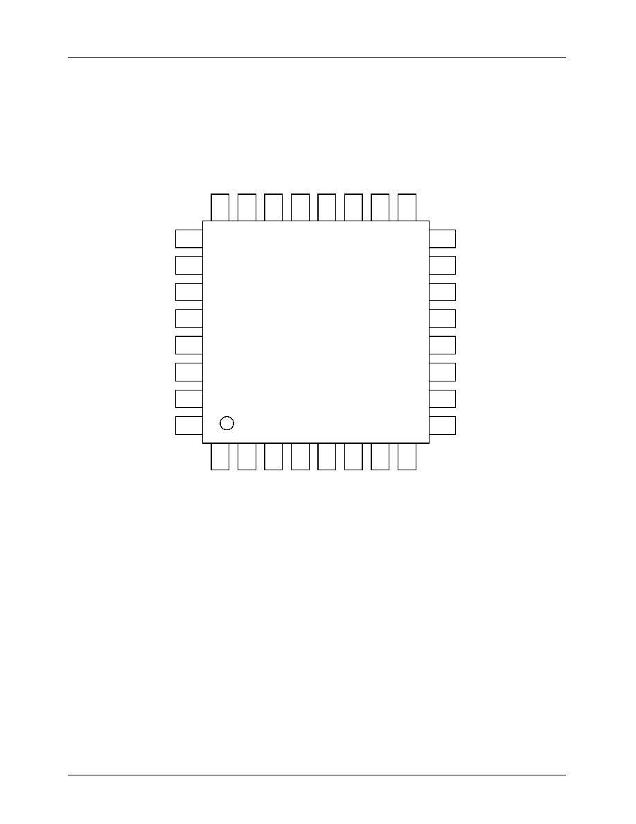
32-LQFP-0707
FAN8700
Camera Motor Drive and Control IC
Typical Applications
∑ Camera system
Ordering Information
Device
Package
Operating Temp.
FAN8700
32-LQFP-0707
-20
∞
C ~ +60
∞
C
FAN8700
2
Pin Assignments
FAN8700
24
23
22
21
20
19
18
17
16
15
14
13
12
11
10
9
8
7
6
5
4
3
2
1
25
26
27
28
29
30
31
32
FMI
DAT1
DAT2
RBT
SGND
VCC
VDI
VDD
VSM
DM2
DM3
NC
PGND
SM1
SM2
SM 5
SM4
FBR
IRO
SVE
PVE
FM
O
PG
ND
DM
1
SEL
CT
L
1
CT
L
2
CT
L
3
PV
E
PG
ND
SM3
PGND
FAN8700
3
Pin Definitions
Pin Number
Pin Name
Pin Function Description
1
SEL
IC Enable Input
2
CTL
1
Operating Mode Control Input1
3
CTL
2
Operating Mode Control Input2
4
CTL
3
Operating Mode Control Input3
5
PGND
Power Ground
6
PV
E
Power V
E
7
PGND
Power Ground
8
SM
3
Stepping Motor Output3
9
SM
4
Stepping Motor Output4 /AE Meter Output
10
SM
5
Stepping Motor Output5 /AE Meter Output
11
SM
2
Stepping Motor Output2
12
SM
1
Stepping Motor Output1
13
PGND
Power Ground
14
NC
No Connection
15
DM
3
DC Motor Output 3
16
DM
2
DC Motor Output 2
17
DM
1
DC Motor Output 1
18
PGND
Power Ground
19
FMO
Step-up Converter Switching Output
20
PV
E
Power V
E
21
SV
E
Signal V
E
22
IRO
IRED drive output
23
FBR
IRED Drive Current Setting Input
24
FMI
Step-up converter switching Clock input
25
DAT
1
Each Mode Output Control Input1
26
DAT
2
Each Mode Output Control Input2
27
RBT
V
E
Voltage Divided Output
28
SGND
Signal Ground
29
V
CC
Low Drop-out Regulator Output
30
V
DI
Setp-up Output Voltage Feedback Input
31
V
DD
Low Drop-out Regulator Output
32
VSM
Stepping Motor Output Voltage Control Input

FAN8700
4
Internal Block Diagram
CONTROL
LOGIC
32
8
9
10
11
12
1
2
3
4
25
26
27
24
6 20 21
7 13
28
17
15
16
29
31
22
23
19
30
SEL CTL
1
CTL
2
CTL
3
DAT
1
RBT FMI
VSM
FMO
VDI
P_GND
S_GND
PVE
SVE
SM3
SM4
SM5 SM2
SM1
IRO
FBR
DM3 DM2 DM1
VCC
VDD
STEP-UP
CONTROL
VDD/VCC
REGULATOR
IRED
FEEDBACK
DRIVER
STEPPING MOTOR
VOLTAGE CONTROL
18
14
NC
5
DAT
2

FAN8700
5
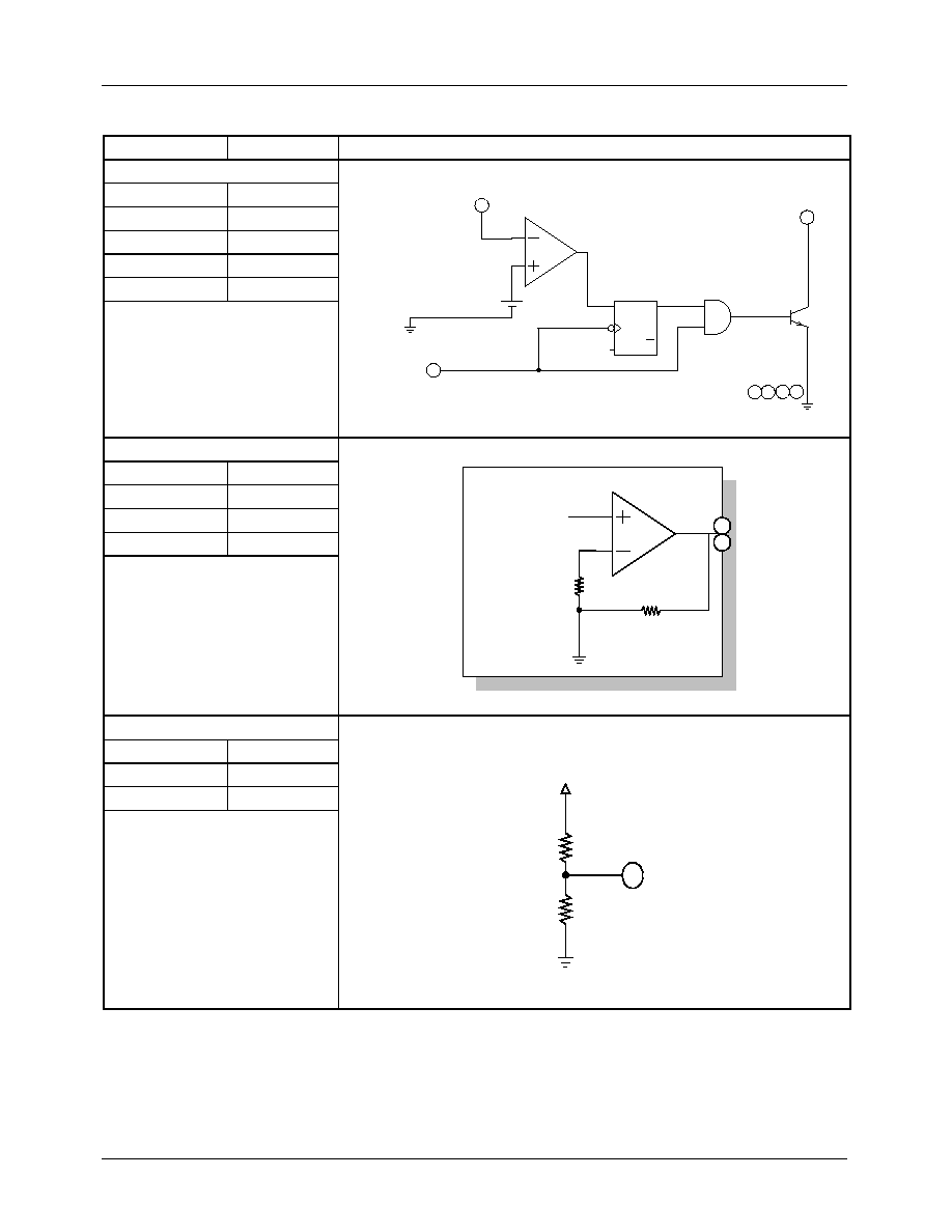
Equivalent Circuits
Description
Pin No.
Internal Circuit
1.5-Channel DC Motor Drive Block
SEL 1
CTL
1
~
3
2~4
DAT
1
~
2
25,26
DM
1
17
DM
2
16
DM
3
15
PVE
6,20
P_GND
5,7,13,18
Step-up Control Block
SEL 1
CTL
1
~
3
2~4
DAT
1
~
2
25,26
SM
1
12
SM
2
11
SM
3
8
SM
4
9
SM
5
10
P_GND
5,7,13,18
IRED Drive Block
SEL 1
CTL
1
~
3
2~4
DAT
1
~
2
25,26
IRO
22
FBR
23
DC Motor Control
Block
CTL1~CTL3
DAT1~DAT2
21
18
4
3
2
20
8
5
P_VE
P_GND
CTL1
26
25
CTL2
CTL3
DAT1
DAT2
17
DM1
16
DM2
15
DM3
M
M
SM4
P_VE
Step Motor
Control Block
CTL1~CTL3
DAT1~DAT2
4
3
2
CTL1
32
26
25
CTL2
CTL3
DAT1
DAT2
VSM
20
6
18
13
P_GND
11
SM2
12
SM1
7
10
SM5
8
SM3
9
2X
5
22
23
IRO
FBR
IRED Control Block
CTL1~3
DAT1~2
4
3
2
26
25
CTL1
CTL2
CTL3
DAT1
DAT2
FAN8700
6
Equivalent Circuits
(Continued)
Description
Pin No.
Internal Circuit
Step-up Control Block
SEL
1
FMI
24
VDI
30
FMO
19
P_GND
5, 7, 13, 18
Regulator Block
SEL
1
VCC
29
VDD
31
P_GND
5, 7, 13, 18
RBT Block
SEL
1
RBT
27
P_GND
5, 7, 13, 18
FMI
30
24
VDI
Vref
D
Q
Q
P_GND
FMO
19
13
7
18
5
INTERNAL
REFERENCE
VOLTAGE
VDD
R
R
29
31
VCC
RBT
R
R
PVE
27
FAN8700
7
Absolute Maximum Ratings (Ta=25
∞
∞
∞
∞
C)
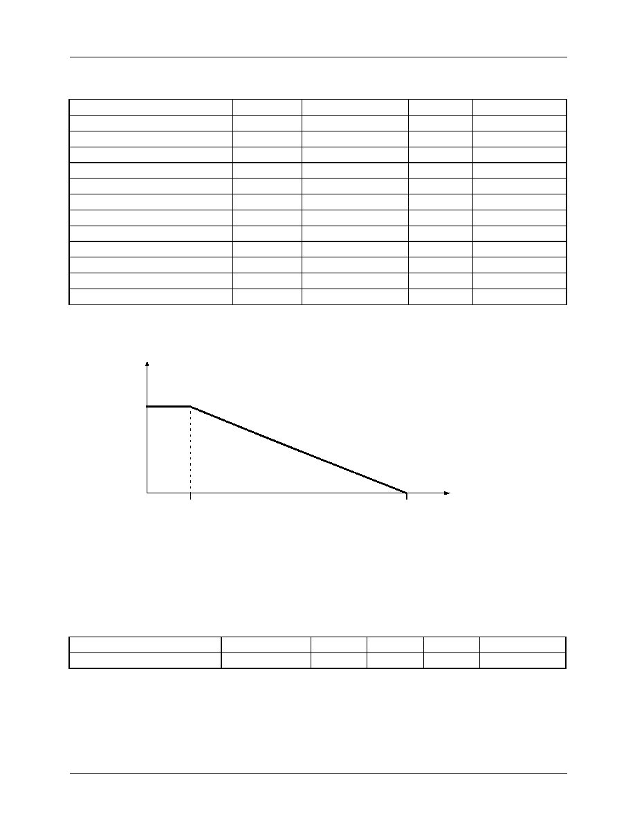
Power Dissipation Curve
Note:
Note:
Note:
Note:
1. PCB Information (Ref. EIA/JSED51-3 and EIA/JSED51-7)
2. Board Layer : 1 Layer
3. Board Thickness : 1.6mm
4. Board Dimension : 76.2 X 114.3 mm
Recommended Operating Conditions (Ta = 25
∞
∞
∞
∞
C)
Parameter
Symbol
Value
Unit
Remark
Supply voltage
V
E
4.5
V
-
V
CC
output current
I
VCC
50
mA
-
V
DD
output current
I
VDD
80
mA
-
Stepping motor output current
I
SM1,2,3,4,5
500
mA
-
DC motor output current
I
DM
2000
mA
500ms
IRED output current
I
IRED
2000
mA
(3000mA/10mS)
Output terminal voltage
V
OUT
5.5
V
500us
Input terminal voltage
V
IN
5.5
V
-
Power dissipation
P
D
1.9
W
-
Thermal resistance
Rja
65
o
C/W
-
Operating temperature range
T
OPR
-20 ~ +60
∞
C
-
Storage temperature range
T
STG
-55 ~ +125
∞
C
-
Parameter
Symbol
Min.
Typ.
Max.
Unit
Operating supply voltage
V
E
2.0
-
4.0
V
Power dissipation (W)
1.9
25
150
Ambient temperature, Ta (
∞
C)

FAN8700
8
Electrical Characteristics
(Ta = -20
∞
C ~ 60
∞
C, V
E
= 2V)
Block
Characteristics
Symbol
Condition
Min. Typ. Max.
Unit
Total
Leakage Current
I
STB
V
E
= 4.0V,V
SEL
= 0V
-
-
1.0
mA
Input Threshold Voltage
V
IT
-
0.75 1.1
1.5
V
Input High Current
I
IH
V
IH
= 3V
-
-
150
mA
Step-up
&
DC-DC
CONVERTER
Minimum Operating Voltage
V
OPR1
-
-
-
1.0
V
Step-up Output Voltage 1
V
VDI1
I
LOAD
=100mA
5.3
5.5
5.7
V
Step-up Output Voltage 2
V
VDI2
I
LOAD
=100mA
8.3
8.6
8.9
FMO Output Voltage 1
V
SAT1/1
I
LOAD
=700mA
-
-
0.3
V
FMO Output Voltage 2
V
SAT1/2
I
LOAD
=1000mA
-
-
0.4
FMI Step-up Clock Range
f
-
39
156 313
KHz
Regulator
V
DD
Output Voltage
V
DD
I
VDD
=60mA
2.85 3.0 3.15
V
V
DD
Drop-out Voltage
V
SAT2/1
I
VDD
=60mA,V
DD
=2V
-
-
0.3
V
CC
Output Voltage
V
CC
I
VCC
=40mA
4.8 5.00 5.2
V
V
CC
Drop-out Voltage
V
SAT2/2
I
VCC
=40mA,V
CC
=3V
-
-
0.3
V
RBT
Minimum Operating Voltage
V
OPR3
-
-
-
1.5
V
Stand-by Output Voltage
V
STB
V
E
=4V,V
SEL
=0V -
-
0.1
V
Output Voltage
V
RBT
-
0.47 0.5 0.53
◊
V
E
Output Voltage Temperature
Coefficient
V
T
-
-
-
2.0
mV/
∞
C
DC Motor
Minimum Operating Voltage
V
OPR4
-
-
-
1.0
V
Output Saturation Voltage
V
SAT4
V
E
=1.6V,I
DM
=400mA
-
-
0.45
V
Step motor
Driver
Minimum Operating Voltage
V
OPR5
-
-
-
1.6
V
Output Saturation Voltage
VSAT5
V
E
=2.6V,I
SM
=
500
mA
-
-
0.7
V
Output Voltage Relative
Difference
DV
V
E
=2.6V
V
SM
=1.0V,R
L
=10
W
SM
1~2
,SM
3~4
-0.1
0
0.1
V
Output Voltage 1
(Output Pin to Ground)
VO
1
V
E
=2.6V,R
L
=10
W,
V
SM
=1.0V
SM
1
,SM
2
,SM
3
,SM
4
1.9
2.0
2.1
V
Output Voltage 2
(Output Pin to Ground)
VO
2
V
E
=2.6V,R
L
=5
W,
V
SM
=1.0V
,
SM
4
,SM
5
1.85 1.95 2.05
V
Ired
Minimum Operating Voltage
V
OPR6
-
-
-
1.5
V
Output Saturation Voltage
V
SAT6
I
IRED
=1000mA
-
-
1.0
V
Output Current
I
IRED
RFBR=0.3
W
0.9
1.0
1.1
A

FAN8700
9
Control Code Table
Mode
Sel
Ctl
1
Ctl
2
Ctl
3
Dat
1
Dat
2
Output Port
Remark
-
-
L
L
L
-
-
-
-
-
-
-
-
-
-
-
-
-
-
SM
1
SM
2
SM
3
SM
4
Stepping
Motor
Drive
H
H
L
H
L
L
L
H
L
H
L
H
L
H
H
L
H
L
H
L
L
H
H
H
H
L
H
L
-
-
-
-
-
-
-
SM4 SM5
-
-
Ae Meter
Drive
H
H
L
L
L
L
OFF OFF
-
-
L
H
H
L
-
-
H
L
L
H
-
-
H
H
L
L
-
-
Ired
H
H
H
H
L
L
-
-
-
-
5.5V Step-up
L
H
-
-
-
-
8.6V Step-up
H
L
-
-
-
-
Ired On Step-up Off
H
H
-
-
-
-
5.5VStep-up
-
-
-
-
-
-
-
CTL DM
1
DM
2
DM
3
-
Dcmotor1
Control
H
L
L
H
L
L
-
OFF OFF OFF
OFF
L
H
-
H
L
OFF
CW
H
L
-
L
H
OFF
CCW
H
H
-
L
L
OFF
Brake
Dcmotor2
Control
H
L
H
L
L
L
-
OFF OFF OFF
OFF
L
H
-
OFF
H
L
CW
H
L
-
OFF
L
H
CCW
H
H
-
OFF
L
L
Brake

FAN8700
10
Test Circuits
9
10
11
12
13
14
15
16
24
23
22
21
20
19
18
17
32
31
30
29
28
27
26
25
FAN8700
SEL
CTL1
CTL2
CTL3
PGND
PVE
PGND
SM3
1
2
3
4
5
6
7
8
SM4
SM5
SM2
SM1
PGND
NC
DM3
DM2
FMI
FBR
IRO
SVE
PVE
FMO
PGND
DM1
VSM
VDD
VDI
VCC
SGND
RBT
DAT2
DAT1
A
sw3
L
L
sw2
sw4
100
10k
H
M
L
sw5
10k
H
L
sw6
10k
H
M
L
10k
100
10k
sw7
sw8
H
M
L
H
M
L
100
10k
sw9
VE
H
L
10k
sw10
H
L
0.2
A
VDI
A
GND
VIN
100
M
H
L
0.25
sw11
I
VDI
I
VE
I
VIN
H
M
M
10k
H
10k
H
L
sw1
M
10k
H
100
V
CC

FAN8700
11
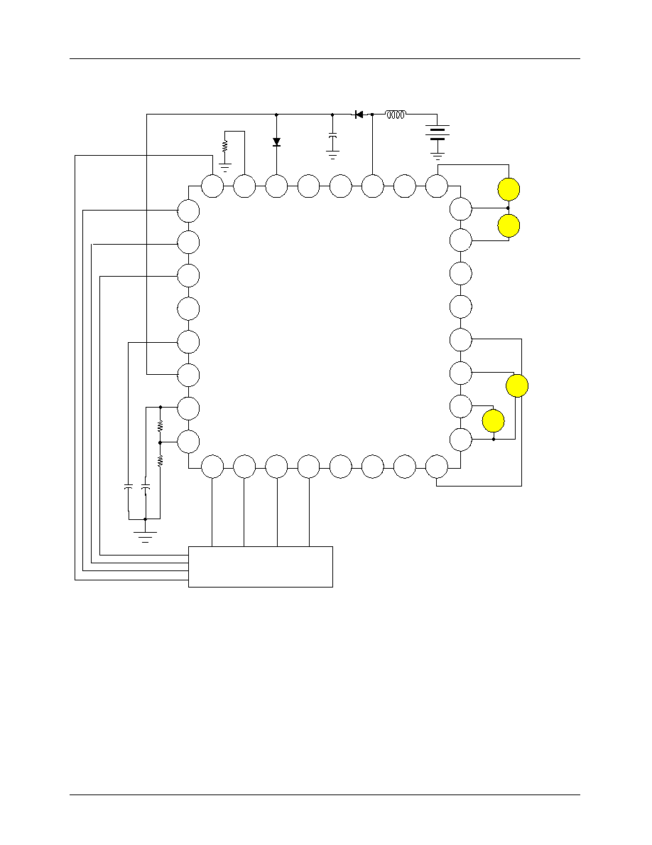
Typical Application Circuits 1
FAN8700
1
4
3
2
5
7
6
26
29
28
27
30
25
32
31
24
21
22
23
20
17
18
19
15
12
13
14
11
16
9
10
M
M
M
Film
Zoom
AF
Actuator
M
Shutter
8
CPU
SEL
CTL1
CTL2
CTL3
PG
PVE
PG
SM3
SM4
SM5
SM2
SM1
PG
NC
DM3
DM2
DM1
PG
FMO
PVE
SVE
IRO
FBR
FMI
DAT1
DAT2
RBT
SG
VCC
VDD
VDI
VSM
PVE&SVE IS
CONNECTED BATTERY
IRED
PG&SG IS
CONNECTED GROUND
FAN8700
12
Typical Application Circuits 2
FAN8700
1
4
3
2
5
7
6
26
29
28
27
30
25
32
31
24
21
22
23
20
17
18
19
15
12
13
14
11
16
9
10
M
M
M
Iris
Zoom
AF
Actuator
M
Shutter
8
CPU
SEL
CTL1
CTL2
CTL3
PG
PVE
PG
SM3
SM4
SM5
SM2
SM1
PG
NC
DM3
DM2
DM1
PG
FMO
PVE
SVE
IRO
FBR
FMI
DAT1
DAT2
RBT
SG
VCC
VDD
VDI
VSM
PVE&SVE IS
CONNECTED BATTERY
LED
PG&SG IS
CONNECTED GROUND

FAN8700
13
Package Dimensions (Unit: mm)
32-LQFP

FAN8700
4/17/02 0.0m 001
Stock#DSxxxxxxxx
" 2002 Fairchild Semiconductor Corporation
LIFE SUPPORT POLICY
FAIRCHILD'S PRODUCTS ARE NOT AUTHORIZED FOR USE AS CRITICAL COMPONENTS IN LIFE SUPPORT DEVICES
OR SYSTEMS WITHOUT THE EXPRESS WRITTEN APPROVAL OF THE PRESIDENT OF FAIRCHILD SEMICONDUCTOR
CORPORATION. As used herein:
1. Life support devices or systems are devices or systems
which, (a) are intended for surgical implant into the
body, or (b) support or sustain life, and (c) whose fail-
ure to
perform when properly used in accordance with
instructions for use provided in the labeling, can be
reasonably expected to result in a significant injury of
the user.
2. A critical component in any component of a life sup-
port
device or system whose failure to perform can be
reasonably expected to cause the failure of the life
support device or system, or to affect its safety or ef-
fectiveness.
www.fairchildsemi.com
DISCLAIMER
FAIRCHILD SEMICONDUCTOR RESERVES THE RIGHT TO MAKE CHANGES WITHOUT FURTHER NOTICE TO ANY
PRODUCTS HEREIN TO IMPROVE RELIABILITY, FUNCTION OR DESIGN. FAIRCHILD DOES NOT ASSUME ANY
LIABILITY ARISING OUT OF THE APPLICATION OR USE OF ANY PRODUCT OR CIRCUIT DESCRIBED HEREIN; NEITHER
DOES IT CONVEY ANY LICENSE UNDER ITS PATENT RIGHTS, NOR THE RIGHTS OF OTHERS.