©2004 Fairchild Semiconductor Corporation
www.fairchildsemi.com
Rev.1.0.3
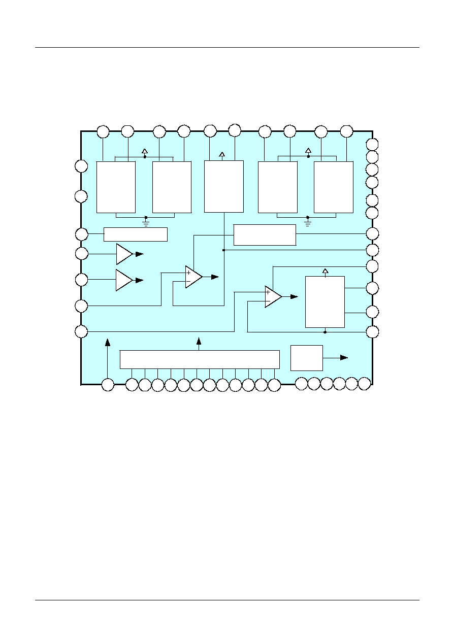
Features
∑ Independent 6-Channel H-Bridge.
∑ Output Current up to 600mA (Each Channel)
∑ Constant Current Control on CH5 and CH6.
∑ Constant Voltage Control on CH1,2,3 and CH4.
∑ Built in Brake Function on CH3,4 and CH6.
∑ Built in Short Through Protection.
∑ Low Saturation Voltage.
∑ Low Voltage operation.
∑ Built in Reference Voltage.
∑ Built in Thermal Shut Down.
Description
The FAN8702 is designed for portable equipment such as
DSC and mobile phone camera. It consists of 2 constant
current and 4 constant voltage drive blocks suitable for shut-
ter, auto-focus, iris and zoom motor drive.
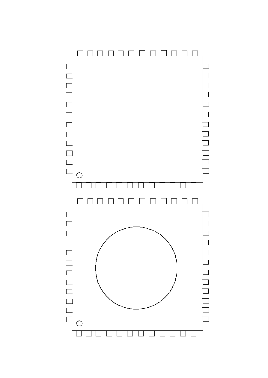
48-LQFP-0707
48MLP7X7
Typical Applications
∑ DSC
∑ Mobile Phone Camera
Ordering Information
Notes
X : Tape & Reel
Device
Package
Operating Temp.
FAN8702MP
48MLP 7X7
-20
∞
C to +80
∞
C
FAN8702MPX
48MLP 7X7
-20
∞
C to +80
∞
C
FAN8702
48-LQFP-0707
-20
∞
C to +80
∞
C
FAN8702B
48-LQFP-0707
-20
∞
C to +80
∞
C
FAN8702/FAN8702B/FAN8702MP
6 Channel DSC Motor Driver

FAN8702/FAN8702B/FAN8702MP
3
Pin Definitions
Pin Number
Pin Name
I/O
Pin Function Description
Remark
FAN8702/B
FAN8702MP
1
12
IN 1
I
Logic Input 1
-
2
11
IN 2
I
Logic Input 2
-
3
10
IN 3
I
Logic Input 3
-
4
9
IN 4
I
Logic Input 4
-
5
8
IN 5
I
Logic Input 5
-
6
7
IN 6
I
Logic Input 6
-
7
6
IN 7
I
Logic Input 7
-
8
5
IN 8
I
Logic Input 8
-
9
4
IN 9
I
Logic Input 9
-
10
3
IN 10
I
Logic Input 10
-
11
2
IN 11
I
Logic Input 11
-
12
1
IN 12
I
Logic Input 12
-
13
48
INHD
I
Voltage Adjust for Vref
-
14
47
SG
P
Signal Ground
-
15
46
NC
-
Non Connection
-
16
45
VDD
P
Supply Voltage (Logic Voltage)
-
17
44
FC2
A
Compensation 2
-
18
43
FC1
A
Compensation 1
-
19
42
NC
-
Non Connection
-
20
41
VCC2
P
Supply Voltage (Current Drive2)
-
21
40
VB2
P
Supply Voltage (Voltage Drive2)
-
22
39
NC
-
Non Connection
-
23
38
PG
P
Power Ground
-
24
37
OUT8
A
Voltage Driver OUT8
-
25
36
OUT7
A
Voltage Driver OUT7
-
26
35
OUT6
A
Voltage Driver OUT6
-
27
34
OUT5
A
Voltage Driver OUT5
-
28
33
OUT12
A
Current Driver OUT12
-
29
32
RFG2
Current Sensing2
-
30
31
OUT11
A
Current Driver OUT11
-
31
30
OUT10
A
Current Driver OUT10
-
32
29
RFG1
Current Sensing1
-
33
28
OUT9
A
Current Driver OUT9
-
34
27
OUT4
A
Voltage Driver OUT4
-
35
26
OUT3
A
Voltage Driver OUT3
-
36
25
OUT2
A
Voltage Driver OUT2
-
37
24
OUT1
A
Voltage Driver OUT1
-
38
23
PG
P
Power Ground
-
39
22
NC
-
Non Connection
-
40
21
VB1
P
Supply Voltage (Voltage Drive1)
-

FAN8702/FAN8702B/FAN8702MP
4
Pin Definitions
(Continued)
Pin Number
Pin Name
I/O
Pin Function Description
Remark
Pin Number
Pin Number
41
20
VCC1
P
Supply Voltage (Current Drive1)
-
42
19
VREF
A
Reference Voltage Out
-
43
18
VC1
A
Voltage Adjust for Out 1~4
-
44
17
VC2
A
Voltage Adjust for Out 5~8
-
45
16
ISH
Voltage Adjust for
Shutter(Out9~10)
-
46
15
IAE
A
Voltage Adjust for IRIS(Out11~12)
-
47
14
NC
-
Non Connection
-
48
13
NC
-
Non Connection
-