©2005 Fairchild Semiconductor Corporation
1
www.fairchildsemi.com
March 2005
FAN8705 Rev. 1.0.1
F
A
N
8705
5 Channel
DS
C Motor Dri
ver
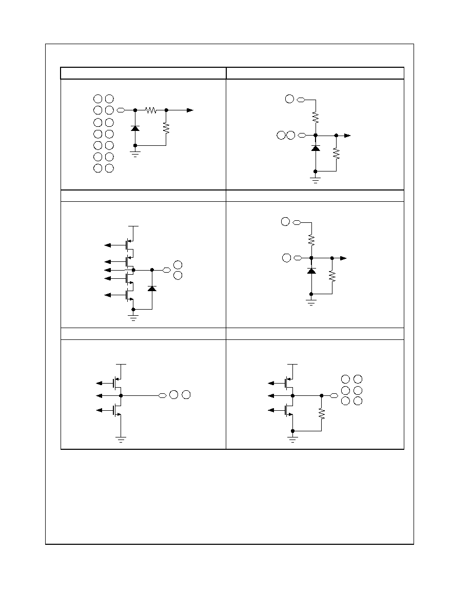
Features
n Built in power save function
n Built in UVLO function.
n Constant current drive for shutter.
n Low Ron resistance (1.1
@ 0.2A
)
n Constant voltage drive for CH1~CH3.
n Pseudo sinewave control for AF.
n Three input 2-2 phase control for AF
n Built in short circuit protection.
n TSD protection.
Applications
n DSC, Mobile phone camera
Description
The FAN8705 is a DSC lens motor driver and it's consist of con-
stant current and constant voltage drive blocks suitable for shut-
ter, single iris,auto-focus and zoom motor drive.
Ordering Information
Device
Package
Operating Temp.
FAN8705
40-MLP
-
25
∞
C ~ 80
∞
C
40MLP5X5
FAN8705
5 Channel DSC Motor Driver
3
www.fairchildsemi.com
FAN8705 Rev. 1.0.1
F
A
N
8705 5
C
h
annel
D
S
C M
o
t
o
r
D
r
i
ver
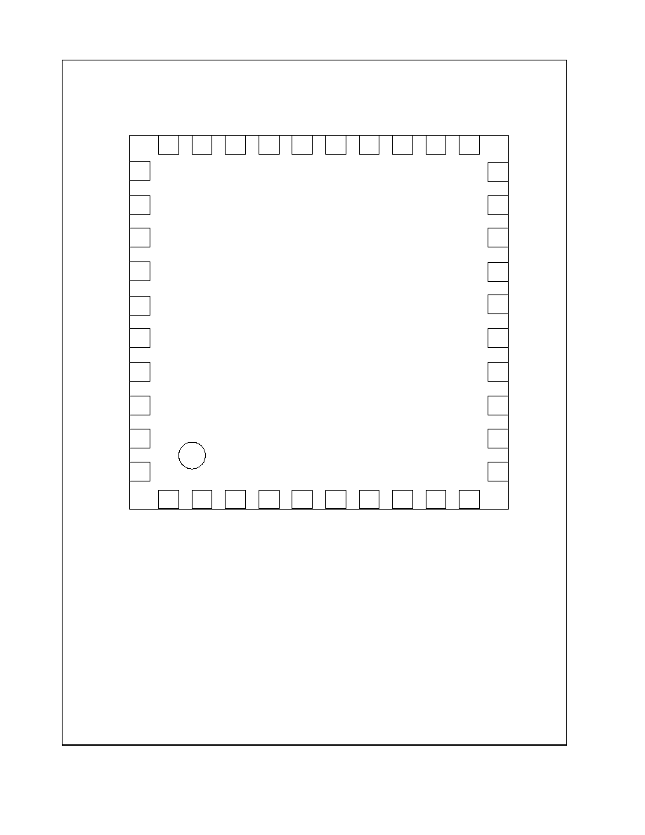
Pin Definitions
Pin Number
Pin Name
I/O
Pin Function Description
Remark
1
IN10
I
Logic input 10
2
PGND1
P
Power ground 1 for Out 1~4
3
OUT1
A
Motor output 1
4
OUT2
A
Motor output 2
5
OUT3
A
Motor output 3
6
OUT4
A
Motor output 4
7
OUT9
A
Motor output 9
8
OUT10
A
Motor output 10
9
FC1
A
Compensation 1
10
RS
A
Motor current sensing for Out9~10
11
FC2
A
Compensation 2
12
GAIN3
I
Gain select for Out9~10
13
VM4
P
Power supply for Out9~10
14
GAIN2
I
Gain select for Out5~6
15
GAIN1
I
Gain select for Out1~4
16
VM3
P
Power supply for Out7~8
17
VDD
P
Logic power supply
18
SEL
I
CH1,2 logic input change
19
PS
I
Power save
20
ADJ3
A
Out9~10 current adjust
21
ADJ2
A
Out5~6 voltage adjust
22
ADJ1
A
Out1~4 voltage adjust
23
VREF
A
Reference output
24
SGND
P
Signal ground
25
OUT8
A
Motor output 8
26
OUT7
A
Motor output 7
27
OUT6
A
Motor output 6
28
OUT5
A
Motor output 5
29
PGND2
P
Power ground 2 for Out5~8
30
IN1
I
Logic input 1
31
IN2
I
Logic input 2
32
IN3
I
Logic input 3
33
VM2
P
Power supply for Out5~6
34
IN4
I
Logic input 4
35
IN5
I
Logic input 5
36
IN6
I
Logic input 6
37
IN7
I
Logic input 7
38
VM1
P
Power supply for Out1~4
39
IN8
I
Logic input 8
40
IN9
I
Logic input 9