ChipFind - документация

Электронный компонент: FAN8728

Скачать:  PDF   ZIP
2002 Fairchild Semiconductor Corporation
www.fairchildsemi.com
Rev. 1.0.0
Features
!
! " !
#$ "% ""
&'($)*+$,$#
" ",-,.
Description
/012*1" "3 %
# " 4+%"
+" +, "
" % & 5/!&5/!0/.6/60
"7" -
48-QFPH-1414
Typical Applications
&"4 7
. "4 7
&"4 7
07"
Ordering Information
Device
Package
Operating Temp
FAN8728
48-QFPH-1414
-
5
C ~ 8
C
FAN8728
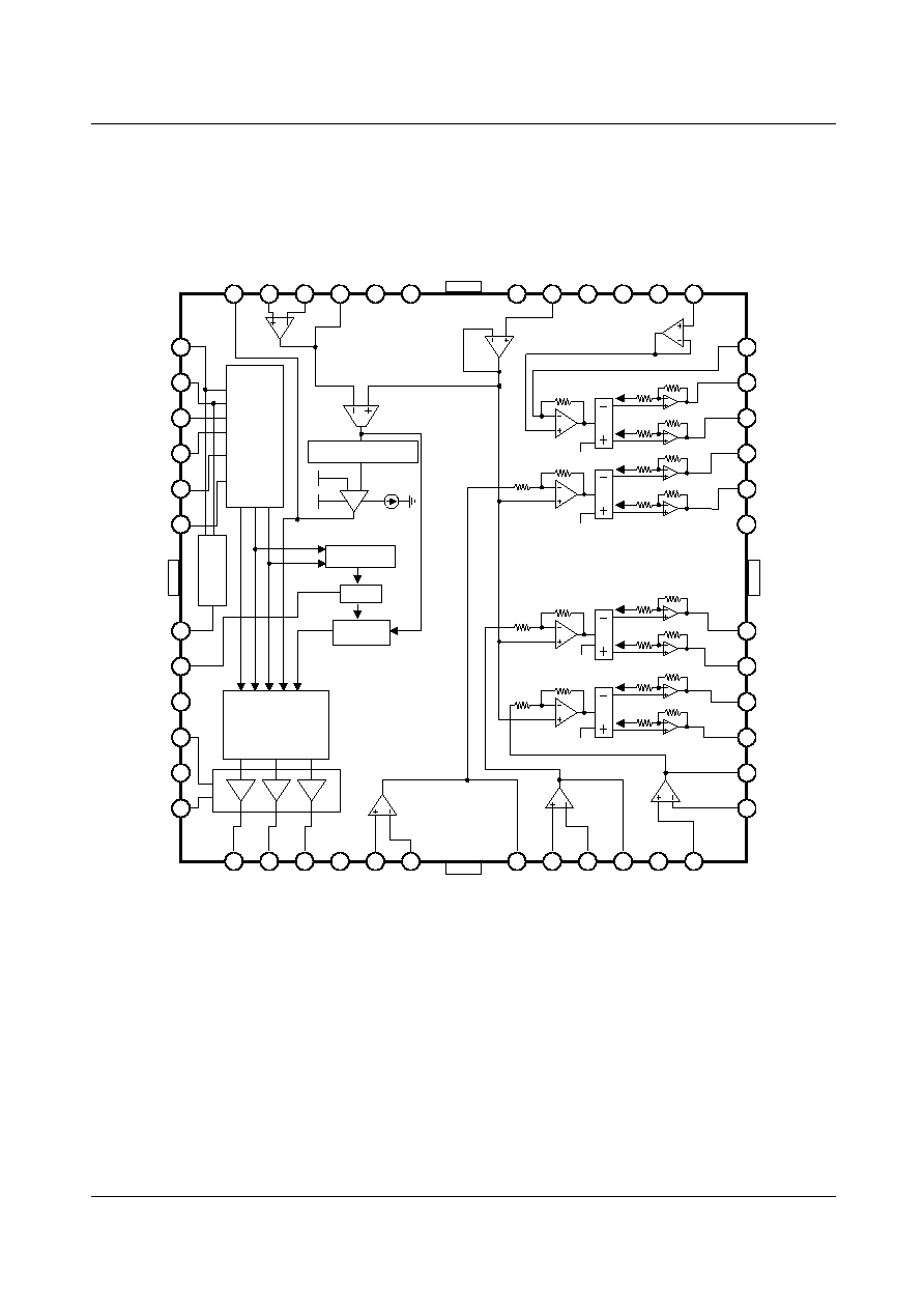
Spindle + 4-CH Input PWM Motor Drive IC
FAN8728
2
Pin Assignments
1
2
3
4
5
6
48
47
46
45
44
43
42
40
39
38
41
37
36
35
34
33
32
31
30
28
27
26
29
25
13
14
15
16
17
18
19
21
22
23
20
24
7
8
9
10
11
12
FAN8728
3
Pin Definitions
Pin Number
Pin Name
I/O
Pin Function Descrition
1
H1+
I
Hall1(+) Input
2
H1-
I
Hall1(-) Input
3
H2+
I
Hall2(+) Input
4
H2-
I
Hall2(-) Input
5
H3+
I
Hall3(+) Input
6
H3-
I
Hall3(-) Input
7
FG
O
FG Output
8
DIR
O
Direction
9
SVCC1
-
SIGNAL VCC1
10
VM1
-
Motor Power Supply
11
CS1
I
Current Sensor
12
PGND1
-
Power Ground
13
A3
O
3-Phase Output 3
14
A2
O
3-Phase Output 2
15
A1
O
3-Phase Output 1
16
SGND
-
Signal Ground
17
IN3+
I
Op-amp CH3 Input(+)
18
IN3-
I
Op-amp CH3 Input(-)
19
OUT3
O
Op-amp CH3 Output
20
IN2+
I
Op-amp CH2 Input(+)
21
IN2-
I
Op-amp CH2 Input(-)
22
OUT2
O
Op-amp CH2 Output
23
VM2
-
BTL CH1,2 Supply Voltage
24
IN2+
I
Op-amp CH2 Input(+)
25
IN2-
I
Op-amp CH2 Input(-)
26
OUT2
O
Op-amp CH2 Output
27
DO1+
O
BTL Drive 1 Output(+)
28
DO1-
O
BTL Drive 1 Output(-)
29
DO2+
O
BTL Drive 2 Output(+)
30
DO2-
O
BTL Drive 2 Output(-)
31
PGND2
-
BTL Power Gnd
32
DO3+
O
BTL Drive 3 Output(+)
33
DO3-
O
BTL Drive 3 Output(-)
FAN8728
4
Pin Definitions
(Continued)
Pin Number
Pin Name
I/O
Pin Function Descrition
34
DO4+
O
BTL Drive 4 Output(+)
35
DO4-
O
BTL Drive 4 Output(-)
36
IN4
I
BTL CH4 Input
37
VREF4
I
BTL CH4 Reference
38
VM4
-
BTL CH4 Motor Supply
39
VM3
-
BTL CH3 Motor Supply
40
SVCC2
-
BTL Signal VCC
41
VREF123
I
BTL CH1,2,3 Rference
42
MUTE123
I
BTL CH1,2,3 Mute
43
MUTE4
I
BTL CH4 Mute
44
SS
I
Spindle Start/Stop
45
OUTS
O
Opamp Spindle Output
46
INS-
I
Opamp Spindle Input(-)
47
INS+
I
Opamp Spindle Input(+)
48
PC1
I
Phase Compesation Cap.
FAN8728
5
Internal Block Diagram
48
45
46
47
43
44
42
41
40
39
38
37
13
16
15
14
18
17
19
20
21
22
23
24
36
33
34
35
31
32
30
29
28
27
26
25
1
4
3
2
6
5
7
8
9
10
11
12
Distributor
Driver
PGND1
CS1
SVCC1
VM1
DIR
FG
H3+
H2-
H2+
H1+
H1-
H3-
PC1
INS-
INS+
A3
A2
A1
VM3
DO3-
SVCC2
M
U
T
E
123
Hall Amp
DO3+
DO2-
DO2+
Absolute Values
Current
Sense Amp
Output
Current Limit
CS1
VM1
FG1X
Generator
Logic
Detection
Reverse
Rotation
PGND2
IN3+
IN2+
IN2-
SGND
OUT2
IN1+
IN3-
OUT3
SS
MUTE4
(LOADING)
DO1-
DO1+
OUT1
VM4
VM3
VM2
VM2
FIN(GND)
FIN(GND)
FIN(GND)
FIN(GND)
VM2
IN1-
VM4
IN4
DO4+
DO4-
VREF4
OUTS
VREF123