
©2003Fairchild Semiconductor Corporation
www.fairchildsemi.com
Rev. 1.0.0
Features
∑ Built-in Power Save Circuit
∑ Built-in Current Limit Circuit
∑ Built-in Thermal Shutdown Circuit (TSD)
∑ Built-in TSD Monitor Circuit
∑ Built-in FG Signal Output Circuit
∑ Built-in Rotational Direction Detecting Circuit
∑ Built-in Protection Circuit For Reverse Rotation
∑ Built-in 4-CH Balanced Transformerless (BTL) Driver
∑ Built-in BTL MUTE Circuit (CH123 and CH4)
∑ Corresponds to 3.3V DSP
Description
The FAN8729 is a monolithic integrated circuit built-in
4Channel BTL motor and spindle motor drivers, which can
drive tracking actuator, focus actuator, sled motor, loading
motor, 3-phase BLDC motor, and it is applicable to DVD-P/
MDP/CAR-MD/CAR-NAVIGATION systems.
48-QFPH-1414
FAN8729
Spindle+4-CH Motor Drive IC
Typical Application
∑ Mini Disk Player
∑ Digital Video Disk Player
∑ Car Mini Disk Player
∑ Car navigation System
Ordering Information
*Note:
NL: Lead free Type
Device
Package
Operating Temperature
FAN8729
48-QFPH-1414
-35
∞C ~ +85∞C
FAN8729_NL*
note
48-QFPH-1414
-35
∞C ~ +85∞C

FAN8729
2
Pin Assignments
DO4-
DO3-
DO3+
NC
PGND2
DO4+
MUTE
4
SS
IN
S-
OU
T
S
PC
1
IN
S
+
VR
E
F
4
SV
CC
2
VM
3
MU
TE1
2
3
VR
EF
12
3
VM4
H1+
PGND1
FG
DIR
SVCC1
VM1
CS1
A3
TS
D
_
M
A1
SG
ND
NC
A2
DO2+
OPOUT
DO1-
DO1+
OPIN-
IN
3
IN
4
OP
IN
+
IN
1
IN
2
VM2
1
2
3
4
5
6
48
47
46
45
44
43
42
40
39
38
41
37
36
35
34
33
32
31
30
28
27
26
29
25
13
14
15
16
17
18
19
21
22
23
20
24
7
8
9
10
11
12
FAN8729
H1-
H2+
H2-
H3+
H3-
DO2-

FAN8729
3
Pin Definitions
Pin Number
Pin Name
I/O
Pin Function Description
1
H1+
I
Hall1(+) Input
2
H1-
I
Hall1(-) Input
3
H2+
I
Hall2(+) Input
4
H2-
I
Hall2(-) Input
5
H3+
I
Hall3(+) Input
6
H3-
I
Hall3(-) Input
7
FG
O
FG Output
8
DIR
O
Direction
9
SVCC1
-
Signal VCC1
10
VM1
-
BLDC Motor Power Supply
11
CS1
I
Current Sensor
12
PGND1
-
Power Ground1
13
A3
O
3-Phase Output 3
14
A2
O
3-Phase Output 2
15
A1
O
3-Phase Output 1
16
SGND
-
Signal Ground
17
NC
-
NC
18
TSD_M
O
TSD Monitor
19
IN4
I
CH4 Input
20
IN3
I
CH3 Input
21
IN2
I
CH2 Input
22
IN1
I
CH1 Input
23
VM2
-
BTL CH1,2 Supply Voltage
24
OPIN+
I
Normal OP-AMP Input(+)
25
OPIN-
I
Normal OP-AMP Input(-)
26
OPOUT
O
Normal OP-AMP Output
27
DO1+
O
BTL Drive 1 Output(+)
28
DO1-
O
BTL Drive 1 Output(-)
29
DO2+
O
BTL Drive 2 Output(+)
30
DO2-
O
BTL Drive 2 Output(-)
31
PGND2
-
BTL Power Ground2
32
DO3+
O
BTL Drive 3 Output(+)
33
DO3-
O
BTL Drive 3 Output(-)

FAN8729
4
Pin Definitions
(Continued)
Pin Number
Pin Name
I/O
Pin Function Description
34
DO4+
O
BTL Drive 4 Output(+)
35
DO4-
O
BTL Drive 4 Output(-)
36
NC
-
NC
37
VREF4
I
BTL CH4 Reference
38
VM4
-
BTL CH4 Motor Supply
39
VM3
-
BTL CH3 Motor Supply
40
SVCC2
-
BTL Signal VCC
41
VREF123
I
BTL CH1,2,3 Reference
42
MUTE123
I
BTL CH1,2,3 Mute
43
MUTE4
I
BTL CH4 Mute
44
SS
I
Spindle Start/Stop
45
OUTS
O
OP-AMP Spindle Output
46
INS-
I
OP-AMP Spindle Input(-)
47
INS+
I
OP-AMP Spindle Input(+)
48
PC1
I
Phase Compesation Cap.

FAN8729
5
Internal Block Diagram
FIN(GND)
48
45
46
47
43
44
42
41
40
39
38
37
13
16
15
14
18
17
19
20
21
22
23
24
36
33
34
35
31
32
30
29
28
27
26
25
1
4
3
2
6
5
7
8
9
10
11
12
Distributor
Driver
PGND1
CS1
SVCC1
VM1
DIR
FG
H3+
H2-
H2+
H1+
H1-
H3-
PC
1
IN
S
-
IN
S+
A3
A2
A1
VM
3
DO3-
SV
CC2
MUTE12
3
Hall
Amp
DO3+
DO2-
DO2+
Absolute Values
Current
Sense Amp
Output
Current Limit
CS
1
VM
1
FG1X
Genera
to
r
Logic
Detection
Reverse
Rotation
PGND2
NC
IN3
IN2
SG
ND
IN
1
OP
IN
+
TSD_M
IN
4
SS
MUTE4
DO1-
DO1+
OPOUT
FIN(GND)
FI
N
(
G
N
D
)
FI
N
(
GN
D)
VM
2
OPIN-
VM
4
NC
EC
ECR
DO4+
DO4-
VRE
F
4
OU
T
S
V
R
EF123
23.5dB
23.5dB
17.5dB
17.5dB
TSD_M
20K
10K
20K
VM2
10K
VM3
VM4
20K
5K
20K
5K
VM2

FAN8729
6
Equivalent Circuits
FG Signal Output
Phase Compensation Capacitor
Current Detector
Start/Stop
BTL Drive Mute
BTL Bias Voltage
7
25
0.5K
48
2K
11
5K
44
25
50K
30K
100K
43
25
50K
42
30K
41
25
50
37

FAN8729
7
Equivalent Circuits
(Continued)
3-Phase Rotational Direction Output
BTL Drive Output
3-Phase Output
TSD_M
BTL Input(CH1,2)
BTL Input(CH3,4)
OP-AMP Input
OP-AMP Output
8
25
27 28
29
33
34 35
32
30K
20K
30
13
14
15
15K
18
25
5K
21
22
25
10K
19
20
2K
1K
1K
2K
2K
2K
SVCC
24
25
SVCC
26

FAN8729
8
Absolute Maximum Ratings (Ta=25
∞C)
Note:
1. When mounted on the PCB (phenolic resin material) of which size is 114mm
◊ 76mm x1.6mm.
2. Power dissipation is reduced with the rate of -21.6mW/
∞C for T
A
25
∞C.
3. Do not exceed Pd and SOA.
Recommended Operating Conditions (Ta=25
∞C)
Parameter
Symbol
Value
Unit
Supply Voltage (Spindle Signal)
Supply Voltage (BTL Signal)
Supply Voltage (Spindle Motor)
Supply Voltage (BTL Motor)
Power Dissipation
Operating Temperature Range
Storge Temperature Range
Maximum Output Current (Spindle Part)
Maximum Output Current (BTL Part)
SV
CC1max
SV
CC2max
V
M1max
V
M2,3,4max
Pd
Topr
Tstg
I
OMAXS
I
OMAXB
7
15
15
15
2.7
note
-35 ~ +85
-55 ~ +150
1.3
1
V
V
V
V
W
∞C
∞C
A
A
Parameter
Symbol
Min.
Type.
Max.
Unit
Operating Supply Voltage (Spindle Signal)
SV
CC1
4.5
-
5.5
V
Operating Supply Voltage (BTL Signal)
SV
CC2
4.5
-
13.2
V
Operating Supply Voltage (Spindle Motor)
V
M1
4.5
-
13.2
V
Operating Supply Voltage (BTL Motor)
V
M2,3,4
4.5
-
SV
CC2
V
1,000
2,000
3,000
0
0
25
50
75
100
125
150
175
Ambient Temperature, Ta[ C]
Pd[mW]
SOA

FAN8729
9
Electrical Characteristics
(Unless otherwise specified, Ta=25
∞C
, SV
CC1
=5V, V
M1
=8V, BTL driver part: SVcc
2
=9V, V
M2
=5V, R
L1
=8
,
V
M3
=8V, V
M4
=9V, R
L2
=15
)
Parameter
Symbol
Condition
Min.
Typ.
Max.
Unit
Circuit Current 2
I
CC2
Start/Stop =5V
-
4.5
-
mA
START/STOP
SS On Voltage Range
V
SSON
L-H Circuit On
2.5
-
-
V
SS Off Voltage Range
V
SSOFF
H-L Circuit Off
-
-
1.0
V
HALL AMP
Hall Bias Current
I
HA
-
-
1
5
uA
Common Mode Voltage Range
V
HAR
-
1.5
-
4.0
V
Minimum In Level
V
INH
-
60
-
-
mVpp
TORQUE CONTROL
EC Input Voltage Range
E
C
0.5
-
3.3
V
Offset Voltage (-)
E
COFF-
E
CR
=1.65V
-100
-50
-20
mV
Offset Voltage (+)
E
COFF+
E
CR
=1.65V
20
50
100
mV
Input Current
E
CIN
E
C
=E
CR
=1.65V
-5
-1
-
uA
In/Output Gain
G
EC
E
CR
=1.65V, R
CS
=0.5
0.56
0.71
0.84
A / V
FG
FG Output Voltage (L)
V
FHL
I
FG
=10uA
-
-
0.5
V
Input Voltage Range
V
FGR
Hn+, Hn- Input D-range
1.5
-
4.0
V
OUTPUT BLOCK
Saturation Voltage (Upper TR)
V
OH
I
O
= -300mA
-
0.9
1.6
V
Saturation Voltage (Lower TR)
V
OL
I
O
=300mA
-
0.2
0.6
V
Torque Limit Current
I
TL
R
CS
=0.5
560
700
840
mA
DIRECTION DETECTOR
DIR Output Voltage (L)
V
DIRL
I
DIR
=10uA
-
-
0.5
V

FAN8729
10
Electrical Characteristics
(continued)
(Unless otherwise specified, Ta=25
∞C
, SV
CC1
=5V, V
M1
=8V, BTL driver part: SVcc
2
=9V, V
M2
=5V, R
L1
=8
,
V
M3
=8V, V
M4
=9V, R
L2
=15
)
Note: Guaranteed field.(No EDS/Final test)
Parameter
Symbol
Condition
Min.
Typ.
Max.
Unit
BTL DRIVE PART
Quiescent Circuit Current
I
CC3
-
-
16.5
-
mA
CH MUTE123 Off Voltage
V
MOFF123
Pin42 = Variation
2.5
-
-
V
CH MUTE123 On Voltage
V
MON123
Pin42 = Variation
-
-
1.0
V
CH MUTE4 Off Voltage
V
MOFF4
Pin43 = Variation
2.5
-
-
V
CH MUTE4 On Voltage
V
MON4
Pin43 = Variation
-
-
1.0
V
CH1,2 Actuator Driver (SV
CC2
=9V V
M2
=5V,R
L1
=8
)
Output Offset Voltage
V
OF1,2
V
IN
= 1.65V
-50
-
+50
mV
Maximum Output Voltage1,2
V
OM1,2
V
IN
= 1.65V
3.6
4.0
-
V
Close Loop Voltage Gain
G
VC1,2
f=1kHz, V
IN
= -0.1Vrms
15.5
17.5
19.5
dB
Ripple Rejection Ratio
*
note
RR1,2
f=120Hz, V
IN
= -20dB
-
60
-
dB
Slew Rate 1,2
*
note
SR1,2
f=120Hz, 2Vp-p
-
1.0
-
V/us
CH3 BTL Driver (SV
CC2
=9V, V
M3
=8V, R
L2
=15
)
Output Offset Voltage3
V
OF3
V
IN
= 1.65V
-100
-
+100
mV
Maximum Output Voltage3
V
OM3
V
IN
= 1.65V
6.5
7.0
-
V
Close Loop Voltage Gain
G
VC3
f= 1kHz, V
IN
= -0.1Vrms
21.5
23.5
25.5
dB
Ripple Rejection Ratio3
*
note
RR
3
f= 120Hz, V
IN
= -20dB
-
60
-
dB
Slew Rate 3
*
note
SR
3
f= 120Hz, 2Vp-p
-
1.0
-
V/us
CH4 BTL Driver (SV
CC2
=9V, V
M4
=9V, R
L2
=15
)
Output Offset Voltage4
V
OF4
V
IN
= 1.65V
-100
-
+100
mV
Maximum Output Voltage4
V
OM4
V
IN
= 1.65V
7.0
7.5
-
V
Close Loop Voltage Gain
G
VC4
f= 1kHz, V
IN
= -0.1Vrms
21.5
23.5
25.5
dB
Ripple Rejection Ratio4
*
note
RR
4
f= 120Hz, V
IN
= -20dB
-
60
-
dB
Slew Rate 4
*
note
SR
4
f= 120Hz, 2Vp-p
-
1.0
-
V/us
OP- AMP
Input Offset Voltage
V
OF
-
-20
-
+20
mV
Input Bias Current
I
B1
-
-
-
300
nA
High Level Output Voltage
V
OHOP
-
8
-
-
V
Low Level Output Voltage
V
OLOP
-
-
-
0.1
V
Output Sink Current
I
SINK
-
-
5.5
-
mA
Output Source Current
I
SOURCE
-
-
4.5
-
mA
Open Loop Voltage Gain
*
note
G
VOOP
f= 1kHz, V
IN
= -75dB
-
75
-
dB
Ripple Rejection Ratio
*
note
RR
OP
f= 120Hz, V
IN
= -20dB
-
65
-
dB
Slew Rate
*
note
SR
OP
f= 120Hz, 2Vp-p
-
1
-
V/us
Common Mode Rejection
Ratio
*
note
CMRR
OP
f= 1kHz, V
IN
= -20dB
-
80
-
dB

FAN8729
11
Application Information
1. MUTE Function
∑ MUTE circuit turns BTL output ON/OFF.
∑ When MUTE terminal (pin42, pin43) is OPEN, or terminal voltage is
lower than 1V, BTL is disable.
∑ When MUTE terminal (pin42, pin43) is voltage is higher than 1.5V,
BTL output operates normally.
∑ Feature Table.
2. TSD Function
∑ TSD circuit intercepts all IC output to protect the IC against high
temperatures.
∑ When chip temperature rises above 165
∞C, BTL and spindle output is
disable.
∑ When chip temperature falls below 140
∞C, BTL and spindle output
operates normally.
∑ TSD has hysteresis of 25
∞C.
3. TSD Monitor Function
∑ TSD monitor circuit displays TSD status.
∑ When TSD is ON, pin18 is HIGH.
∑ When TSD is OFF, pin18 is LOW.
∑ Since output pin(PIN18) is open-collector, pull-up resistance should be
attached outside.
∑ Feature Table.
MUTE circuit voltage
MUTE status
Above 1.5V
OFF
Below 1V or Open
ON
TSD Pin18
TSD On
High
TSD Off
Low
42
43
Output driver
Bias
Q0
SVCC
IREF
Hysteresis
R1
R2
R3
Ihys
20k
Q5
Q6
18
TSD
SVCC
VCC
R(external)

FAN8729
12
4. CH1,2,3,4 Balanced Transformerless (BTL) Drive
∑ Diagram above shows each input/output BTL channel structure.
∑ When BTL input voltage is V
ref
, the output voltage is P
ref
. P
ref
has the value of VM/2.
∑ BTL Channel's output voltage is found as follows;
∑ BTL gain value is found as follows;
LEVEL
SHIFT
M
32
34
29 27
33
35
28
30
P
ref
P
ref
37 41
19 20
21 22
Vref123,4
Vin
R2
R1
R3
R3
R3
R3
DO+
DO-
)
(
)
3
3
1
(
1
2
Pr
)
(
)
3
3
1
(
1
2
Pr
Vref
Vin
R
R
R
R
ef
Do
Vref
Vin
R
R
R
R
ef
Do
-
◊
+
◊
-
=
-
-
◊
+
◊
+
=
+
1
2
4
R
R
Gain
◊
=

FAN8729
13
5. Spindle
∑ The spindle driver circuit consists of 3 section: Torque sense amp, Current sense amp, and Power driver.
∑ Torque sense amp compares and amplifies E
C
and E
CR
signals from SERVO, and sends them to current sense amp. With
voltage comparison, it determines the signal as forward or reverse.
∑ Current sense amp limits the current in Motor(Io) by comparing output current signal from torque sense amp with the
current of R
CS
.
∑ Power driver output the current to the motor based on the current generated form current sense amp.
∑ Feature Table
+
-
Torque sense amp
V
AMP
Driver
E
CR
E
C
Rcs
Gain
Controller
TSD
+
-
Current sense amp
V
RCS
Io
M
VM1
VM1
Power Driver
E
CR
-
E
C
[mV]
V
RNF[V]
3mV
-50
0
+50
Reverse
Forward
Ecoff-
Ecoff+
E
C
< E
CR
Rotation
E
C
> E
CR
Forward rotation
Stop after detecting
reverse rotation

FAN8729
14
6. Calculation of Gain & Torque Current
∑ Toque limit circuit limits the current of spindle motor.
∑ Driver amp circuit limits the current of spindle motor by comparing the voltage detected from R
CS
and the voltage output
from torque sense map.
∑ Output current of the motor can be limited by adjusting the R
CS
value.
∑ Maximum output current of motor is found as follows;
∑ VMAX within IC is fixed at 350mV.
∑ Gm of torque sense amp is set to 0.71.
ER
ECR
VM1
Driver
Current / Voltage
Convertor
VM1
Gm
+
-
Power
Transistors
Commutation
Distributor
+
+
-
+
-
Vin
R1
+
-
Vmax
Absolute
Values
Negative
Feedback loop
H2
H3
H1
Max. output
current limiting
U
V
W
Io
VM1
Rcs
CS1(Pin11)
Io
+
-
Vs
Output
Current sense
Rcs
mV
Rcs
V
mA
Io
350
max
]
[
=
=
FAN8729
15
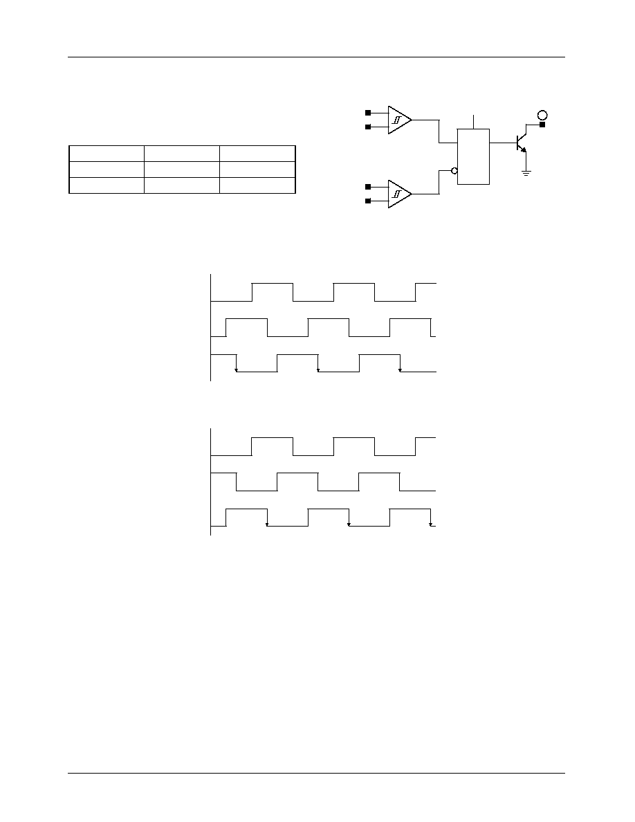
7. Rotational Direction Detecting Function
∑ Rotation detection circuit gives the result to DIR pin by
detecting the MD's rotational direction.
∑ Detects the MD's rotational direction using hall signals H2 and
H3.
∑ Feature Table.
∑ In case of forward rotational detection, the phase of hall signal shows as H3
H2 H1 as follows;
∑ In case of reverse rotational detection, the phase of hall signal shows as H1
H2 H3 as follows;
∑ Forward/Reverse rotational direction is decided as follows. When hall signal H3 is falling edge, if H2 shows "High", the
rotational direction is "Forward", and if H2 shows "Low", rotational direction is "Reverse".
Rotation
DIR
EC < ECR
Forward
Low
EC > ECR
Reverse
High
D
CK
Q
+
-
+
-
R
D-F/F
8
DIR
H2+
H2-
H3+
H3-
H 1
H 2
H 3
(b)
H 1
H 2
H 3
(a)
FAN8729
16
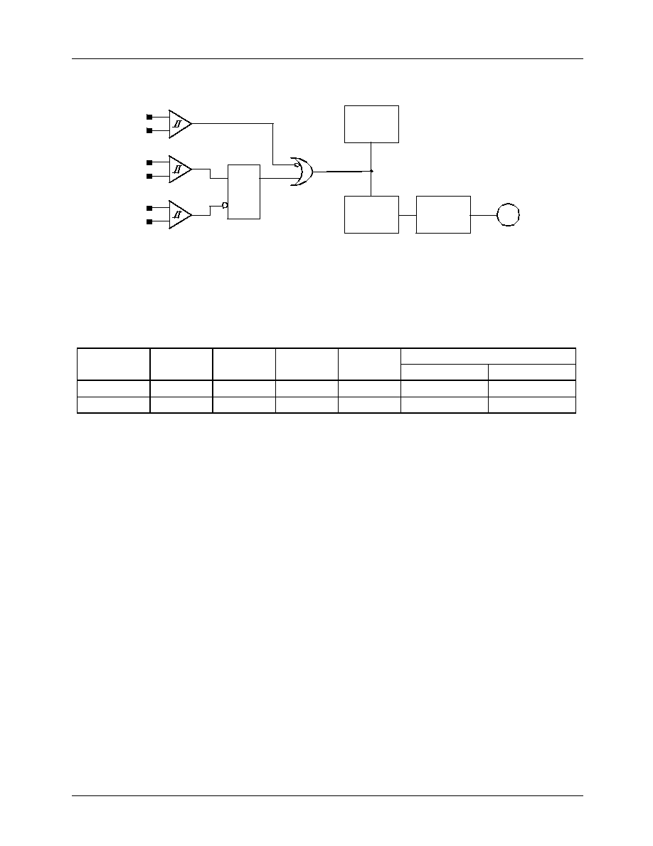
8 Reverse Rotation Preventing Function
∑ Reverse rotation prevention circuit has a function for intercepting the reverse rotation of MD.
∑ When SERVO control input is EC<ECR, MD rotates forward and Q which is the output of D-F/F goes "High".
∑ When SERVO control input is EC>ECR, motor puts on reverse brake and MD speed is rapidly reduced.
∑ When SERVO control input remains EC>ECR, MD rotates reverse and Q which is the output of D-F/F goes "Low", in
result current sense amp is interrupted. Accordingly gain controller goes OFF and motor is stopped.
∑ Feature Table.
Rotation
H2
H3
D-F/F
DIR
Reverse Rotation Preventer
E
C
<E
CR
E
C
>E
CR
Forward
H H
L
H
L
Forward
Brake and Stop
Reverse
L
H
L
L
H
≠
Stop
+
-
+
-
H2+
H2-
H3+
H3-
D
CK
Q
R
D-F/F
+
-
E
C
E
CR
Gain
controller
Current
S ens e
Amp
Driver
M

FAN8729
17
8. FG Output Function
∑ FG circuit outputs the number of motor rotation.
∑ One pulse per rotation is output of FG.
∑ FG uses hall signal H1 as its input, and creates output using hysteresis
comparator.
∑ Input/Output wavelength is shown below;
+
-
FG Output
H1+
H1-
7
H 1
F G

FAN8729
18
9. Hall Input Output Timing Chart
∑ Output voltage and current wavelength of each of the 3-phase hall input is shown below.
∑ The following diagram is the motor's output wavelength in the forward rotation direction.
H1+
H2+
H3+
A1 output current
A1 output voltage
A2 output current
A2 output voltage
A3 output current
A3 output voltage

FAN8729
19
Typical Performance Characteristics
SVCC2 vs ICC3
10.0
11.0
12.0
13.0
14.0
15.0
4.5
5.5
6.5
7.5
8.5
9.5
10.5 11.5 12.5 13.5
SVCC2(V)
ICC3(mA
)
V IN1 vs V OUT1 (V REF=1.65V , V M2=5V )
-6.0
-4.0
-2.0
0.0
2.0
4.0
6.0
0.0
1.0
2.0
3.0
V IN1(V )
VOUT1(V)
V IN2 vs V OUT2 (V REF=1.65V , V M2=5V )
-6.0
-4.0
-2.0
0.0
2.0
4.0
6.0
0.0
0.5
1.0
1.5
2.0
2.5
3.0
V IN2(V )
VOUT2
V IN3 vs V OUT3 (V REF=1.65V , V M3=12V )
-12.0
-8.0
-4.0
0.0
4.0
8.0
12.0
0.0
0.5
1.0
1.5
2.0
2.5
3.0
V IN3(V )
VOUT3(V)
V IN4 vs V OUT4 (V REF=1.65V , V M4=12V )
-12.0
-8.0
-4.0
0.0
4.0
8.0
12.0
0.0
0.5
1.0
1.5
2.0
2.5
3.0
V IN4(V )
VOUT4(V)
SVCC1 vs ICC2
3.00
3.50
4.00
4.50
5.00
5.50
6.00
4.5
4.6
4.7
4.8
4.9
5.0
5.1
5.2
5.3
5.4
5.5
SVCC1(V)
ICC2(mA
)

FAN8729
20
Typical Performance Characteristics
SVCC2 vs GVC1
15.5
16.0
16.5
17.0
17.5
18.0
18.5
19.0
19.5
4.5
5.5
6.5
7.5
8.5
9.5
10.5 11.5 12.5 13.5
SVCC(V)
GCV1(
d
B)
SVCC2 vs GVC2
15.5
16.0
16.5
17.0
17.5
18.0
18.5
19.0
19.5
4.5
5.5
6.5
7.5
8.5
9.5
10.5 11.5 12.5 13.5
SVCC2(V)
GVC2(dB)
SVCC2 vs GVC3
21.5
22.0
22.5
23.0
23.5
24.0
24.5
25.0
25.5
4.5
5.5
6.5
7.5
8.5
9.5
10.5 11.5 12.5 13.5
SVCC2(V)
GVC3(
d
B)
SVCC2 vs GVC4
21.5
22.0
22.5
23.0
23.5
24.0
24.5
25.0
25.5
4.5
5.5
6.5
7.5
8.5
9.5
10.5 11.5 12.5 13.5
SVCC2(V)
GVC4(
d
B)
INS+ vs ITL (V REF=1.65V )
0
200
400
600
800
0.0
0.5
1.0
1.5
2.0
2.5
3.0
INS+(V )
ITL(mA)

FAN8729
21
Test Circuits
FAN8729
A1
SVCC1
H3+
DIR
CS1
H3-
H2-
H2+
H1+
TS
D
_
M
H1-
A2
A3
S
GND
VR
E
F
4
VM
3
DO2+
DO2-
VM
4
VREF12
3
SVC
C
2
MU
T
E
1
2
3
DO3-
DO1+
DO4-
NC
NC
DO1-
DO3+
IN
4
IN
3
IN
2
FG
IN
1
OP
I
N
+ OPIN-
VM1
VM
2
1
2
3
4
5
6
7
8
9
10
11
12
13
14
15
16
17
18
19
21
22
23
20
24
48
47
46
45
44
43
42
40
39
38
41
37
36
35
34
33
32
31
30
28
27
26
29
25
PGND1
SS
OU
TS
INS-
PC1
INS+
MU
T
E
4
PGND2
DO4+
SVCC1
A
VM1
V
A
OPOUT
a
b
c
a
b
c
a
b
c
V
V
V
A
A
A
A
A
A
Hall Signal
Generation
V
V
10uA
V
A
A
V
RL1
RL2
1
2
V
RL1
RL2
1
2
V
RL1
RL2
1
2
V
RL1
RL2
1
2
A
300m
A
3
00m
A
RL
RL
RL
OP
IN+
OP
I
N
-
OP
OUT
OP
IN
+
OP
I
N
-
OP
OUT
V
V
V
V
1M
1M
10
uF
VCC
50
V
OPIN+
OPIN-
OPOUT

FAN8729
22
Typical Application Circuits
Notes:
Radiation pin is connected to the internal GND of the package.
M
Focus
Loadng
VM1
M
Sled
Motor
DO4-
DO3+
DO3-
D04+
PGND2
MU
TE4
SS
INS-
OUT
S
PC
1
INS
+
VRE
F
4
SV
CC2
VM
3
MU
TE
1
2
3
VRE
F
1
2
3
VM
4
H1-
H1+
H2+
H2-
H3+
H3-
PGND1
FG
DIR
SVCC1
VM1
CS1
A3
TS
D
_
M
A1
S
GND
NC
A2
DO2+
OPOUT
DO2-
DO1+
OPIN-
IN
3
IN
4
OP
I
N
+
IN
1
IN
2
VM
2
5
6
48
47
46
45
44
43
42
40
39
38
41
37
36
35
34
33
32
31
30
28
27
26
29
25
13
14
15
16
17
18
19
21
22
23
20
24
7
8
9
10
11
12
FAN8729
DO1-
NC
HALL1
HALL2
HALL3
0.1uF
Tracking
Se
r
v
o
Tor
q
ue
Con
t
rol
Sys
t
e
m
Co
nt
ro
l
CH4
Mu
t
e
CH
123
Mu
t
e
VRE
F
4
VR
EF
Tr
acki
n
g
Foc
u
s
Sl
e
d
Servo Amp
Rotate
Direction
FG
Signal
Lo
ad
i
n
g
1
2
3
4

FAN8729
23
Package Dimensions
#1
#48
(0.825)
17.20
±
0.30
(4.85)
0.10MAX
0.65
14.00
±
0.20
17.20
±
0.30
14.00
±
0.20
+
0.10
-0.05
0.30
0.80
±
0.20
0.10MAX
2.60
±
0.10
3.00MAX
0.00~0.25
0~8
∞
+
0.10
-0.05
0.20
48-QFPH-1414

FAN8729
11/4/03 0.0m 001
Stock#DSxxxxxxxx
2003 Fairchild Semiconductor Corporation
LIFE SUPPORT POLICY
FAIRCHILD'S PRODUCTS ARE NOT AUTHORIZED FOR USE AS CRITICAL COMPONENTS IN LIFE SUPPORT DEVICES
OR SYSTEMS WITHOUT THE EXPRESS WRITTEN APPROVAL OF THE PRESIDENT OF FAIRCHILD SEMICONDUCTOR
CORPORATION. As used herein:
1. Life support devices or systems are devices or systems
which, (a) are intended for surgical implant into the body,
or (b) support or sustain life, and (c) whose failure to
perform when properly used in accordance with
instructions for use provided in the labeling, can be
reasonably expected to result in a significant injury of the
user.
2. A critical component in any component of a life support
device or system whose failure to perform can be
reasonably expected to cause the failure of the life support
device or system, or to affect its safety or effectiveness.
www.fairchildsemi.com
DISCLAIMER
FAIRCHILD SEMICONDUCTOR RESERVES THE RIGHT TO MAKE CHANGES WITHOUT FURTHER NOTICE TO ANY
PRODUCTS HEREIN TO IMPROVE RELIABILITY, FUNCTION OR DESIGN. FAIRCHILD DOES NOT ASSUME ANY
LIABILITY ARISING OUT OF THE APPLICATION OR USE OF ANY PRODUCT OR CIRCUIT DESCRIBED HEREIN; NEITHER
DOES IT CONVEY ANY LICENSE UNDER ITS PATENT RIGHTS, NOR THE RIGHTS OF OTHERS.