©2005 Fairchild Semiconductor Corporation
1
www.fairchildsemi.com
April 2005
FAN8741/FAN8742 Rev. 1.0.1
F
A
N
8741
/F
A
N
8
742
S
p
indl
e mot
o
r
and 6-
CH act
uator dri
ver
FAN8741/FAN8742
FAN8741/FAN8742
FAN8741/FAN8742
FAN8741/FAN8742
Spindle Motor and 6-CH Driver
Spindle Motor and 6-CH Driver
Spindle Motor and 6-CH Driver
Spindle Motor and 6-CH Driver
[Spindle(PWM), Sled 2-CH(PWM) 4-CH(Linear)]
[Spindle(PWM), Sled 2-CH(PWM) 4-CH(Linear)]
[Spindle(PWM), Sled 2-CH(PWM) 4-CH(Linear)]
[Spindle(PWM), Sled 2-CH(PWM) 4-CH(Linear)]
Features
Common
∑ Built-in thermal shutdown circuit (TSD)
∑ 8 Independent voltage sources
∑ Corresponds to 3.3V or 5V DSP
∑ 4 selectable mute inputs
Spindle
∑ Output PWM mode control
∑ FG output: open collector type
∑ Selectable brake(short & reverse brake)
∑ Built-in hall bias
∑ 180
o
commutation(compatible with conventional BLDC spindle
motor)
∑ Built in short-through protection function
BTL(Sled 2-channels)
∑ Output PWM mode control
∑ Built in short-through protection function
BTL(Other 4-channels)
∑ Output linear mode control
Typical Applications
∑ CD-ROM
∑ CD-RW
∑ DVD-ROM
∑ DVD-RAM
∑ DVD Player (DVDP)
∑ Other compact disk media
∑ Game consoles
Description
Suitable for a 3-phase BLDC (Brush-Less Direct Current) spindle
motor driver with PWM, the monolithic FAN8741/FAN8742 IC also
includes 2-ch motor drivers with PWM for sled motors and 4-ch
linear drivers which drive the focus actuator, tracking actuator, tilt
actuator, and loading motor in optical media applications.
Designed specifically for high-speed/high-density optical media
applications, the FAN8741/FAN8742's power stage is created by
D-MOS transistors which have extremely low RDS
ON
. This
enables less heat generation and guarantees improved reliability.
The FAN8741G/FAN8742G is available in a 56-SSOP-HS pack-
age, which has high-power dissipation and the leadframe is
exposed to the top side.
The FAN8741MTF/FAN8742MTF is available in a 56-TSSOP-EP
package, which is very thin and the leadframe is exposed to
the bottom side.
Ordering Information
HS=HeatSlug, EP=ExposedPad
X:Tape & Reel type
FAN8741:FG3X
FAN8742:FG1X
Device
Package
Operating Temp.
FAN8741G
56-SSOP-HS
-
25
∞
C to +75
∞
C
FAN8741GX
56-SSOP-HS
-
25
∞
C to +75
∞
C
FAN8742G
56-SSOP-HS
-
25
∞
C to +75
∞
C
FAN8742GX
56-SSOP-HS
-
25
∞
C to +75
∞
C
FAN8741MTF
56-TSSOP-EP
-
25
∞
C to +75
∞
C
FAN8741MTFX
56-TSSOP-EP
-
25
∞
C to +75
∞
C
FAN8742MTF
56-TSSOP-EP
-
25
∞
C to +75
∞
C
FAN8742MTFX
56-TSSOP-EP
-
25
∞
C to +75
∞
C
2
www.fairchildsemi.com
FAN8741/FAN8742 Rev. 1.0.1
F
A
N
8741
/F
A
N
8
742
S
p
indl
e mot
o
r
and 6-
CH act
uator dri
ver
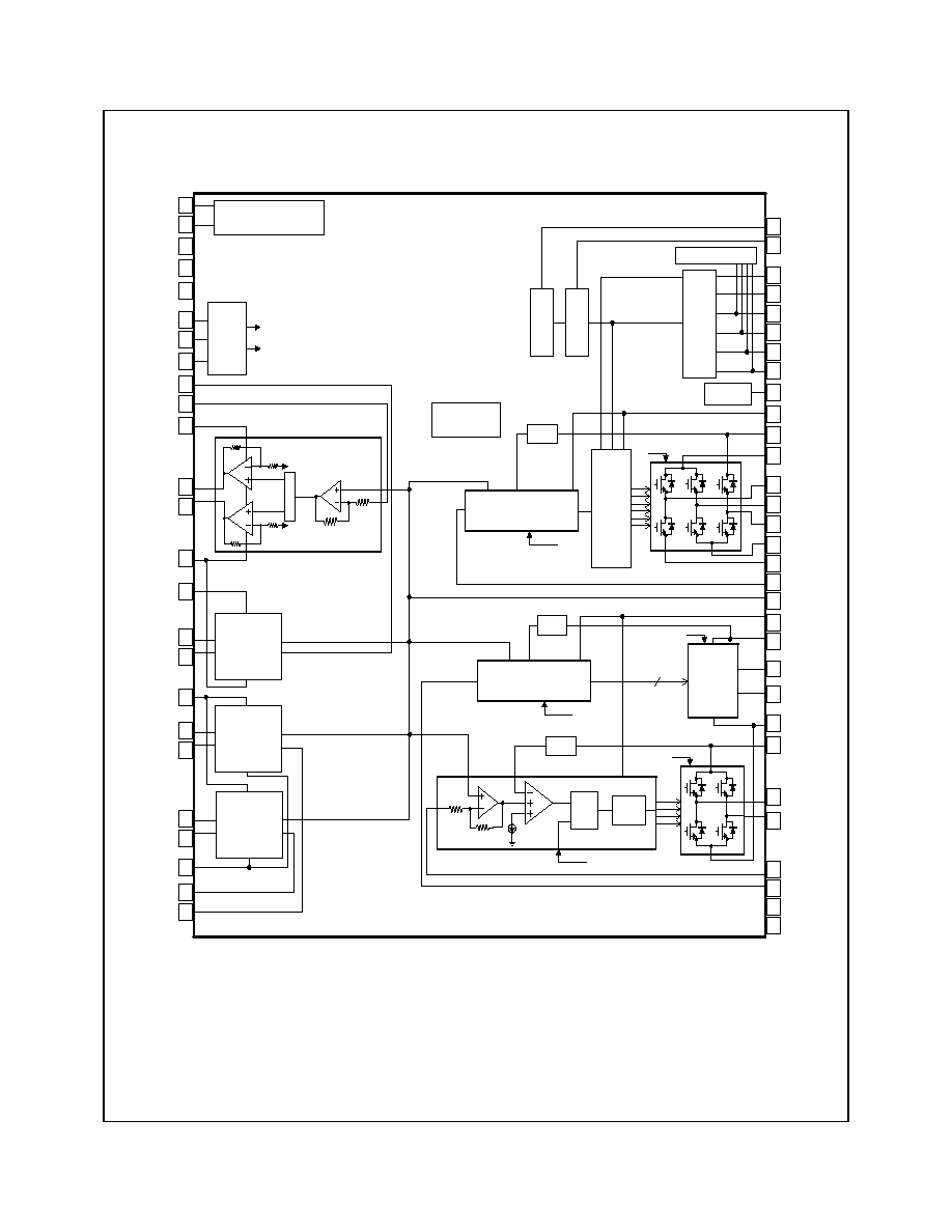
Internal Block Diagram
(Pins numbered according to the FAN8741MTF--Leadframe exposed to the bot
tom)
H-bridge
4
DIR
OSC
OSC
Hall Amp
Com
m
utator
& Pow
e
r dr
ive
Reverse Detect
F
r
egue
nc
y
Ge
n
e
r
a
t
o
r
Sp
i
n
dl
e
Di
r
e
c
t
i
o
n
I
OMAX
Drive
Logic
Flip
Flop
OSC
PWM Control
10k
10k
Lev
el
s
h
i
f
t
20k
10k
BTL driver
43
44
31
40
41
38
39
36
37
32
34
35
BTL
driver
BTL
driver
BTL
driver
33
45
42
46
47
53
54
55
Ch
ar
g
e
pu
m
p
&
O
scil
l
a
t
or
VCP
VCP
VCP
48
REF
PWM Control
OSC
56
H
bridge
PWM Control
52
23
Hall bias
22
Mute Selection
&Spindle brake sel.
TSD
18
19
24
16
17
26
25
29
30
10
12
14
5
6
7
2
3
4
15
11
1
49
50
51
21
13
9
20
27
28
8
FG
HU+
HU
-
HV+
HV
-
HW+
HW
-
VH
VM1
RSP2
RSP1
U
V
W
PGND2
PGND1
SPIN
REF
VM2
RSL1
SL1+
SL1
-
PGND3
RSL2
SL2+
SL2
-
SLIN2
SLIN1
SVCC2
SGND
MUTE1
MUTE2
SVCC1
DGND
VDD
VCP
CP2
CP1
IN3
IN4
PVCC3
DO4
-
DO4+
PGND5
PVCC2
DO3
-
DO3+
PVCC1
DO2
-
DO2+
DO1+
DO1
-
PGND4
IN1
IN2
VCP
LPF
LPF
LPF
3
www.fairchildsemi.com
FAN8741/FAN8742 Rev. 1.0.1
F
A
N
8741
/F
A
N
8
742
S
p
indl
e mot
o
r
and 6-
CH act
uator dri
ver
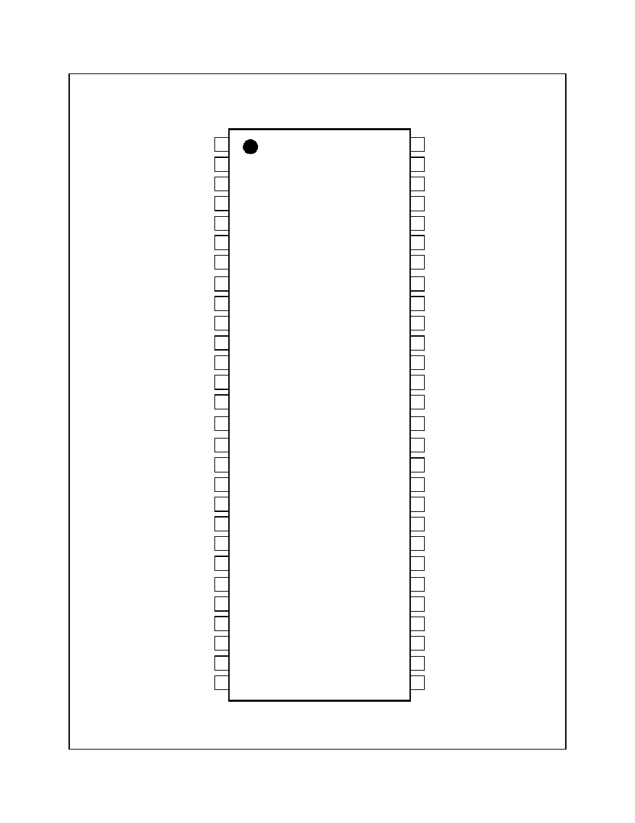
Pin Assignments
(Leadframe exposed to the bottom side)
1
2
3
4
5
6
9
10
11
FAN8741MTF/
12
13
14
7
8
17
18
19
20
21
22
15
16
23
24
25
26
27
28
56
55
54
53
52
51
48
47
46
45
44
43
50
49
40
39
38
37
36
35
42
41
34
33
32
31
30
29
SPIN
VDD
IN3
IN4
PGND5
DO4-
PVCC3
DO3+
DO2-
DO2+
DO1-
DO1+
DO4+
DO3-
IN1
PVCC1
PVCC2
SLIN1
SLIN2
PGND4
IN2
DIR
FG
SVCC1
CP1
CP2
VCP
VM1
HU-
HV+
HV-
HW+
HW-
DGND
HU+
PGND1
RSP1
V
PGND2
W
RSP2
VH
U
SL1-
SL2+
SL2-
PGND3
REF
SL1+
MUTE1
MUTE2
RSL1
RSL2
VM2
SVCC2
SGND
FAN8742MTF
(PAD DOWN)
4
www.fairchildsemi.com
FAN8741/FAN8742 Rev. 1.0.1
F
A
N
8741
/F
A
N
8
742
S
p
indl
e mot
o
r
and 6-
CH act
uator dri
ver
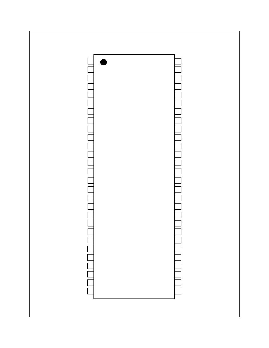
Pin Assignments
(Leadframe exposed to the top side)
1
2
3
4
5
6
9
10
11
FAN8741G/
12
13
14
7
8
17
18
19
20
21
22
15
16
23
24
25
26
27
28
56
55
54
53
52
51
48
47
46
45
44
43
50
49
40
39
38
37
36
35
42
41
34
33
32
31
30
29
SPIN
VDD
IN3
IN4
PGND5
DO4-
PVCC3
DO3+
DO2-
DO2+
DO1-
DO1+
DO4+
DO3-
IN1
PVCC1
PVCC2
SLIN1
SLIN2
PGND4
IN2
DIR
FG
SVCC1
CP1
CP2
VCP
VM1
HU-
HV+
HV-
HW+
HW-
DGND
HU+
PGND1
RSP1
V
PGND2
W
RSP2
VH
U
SL1-
SL2+
SL2-
PGND3
REF
SL1+
MUTE1
MUTE2
RSL1
RSL2
VM2
SVCC2
SGND
FAN8742G
(SHOULD THIS
SAY "PAD UP"
TO MATCH THE
PREVIOUS PAGE?)

5
www.fairchildsemi.com
FAN8741/FAN8742 Rev. 1.0.1
F
A
N
8741
/F
A
N
8
742
S
p
indl
e mot
o
r
and 6-
CH act
uator dri
ver
Pin Definitions
Pin Number
(exposed to bottom)
Pin Number
(exposed to top)
Pin Name
I/O
Pin Function Description
1
56
VM1
P
Power supply for spindle
2
55
HU+
A
Hall signal input(Hu+)
3
54
HU-
A
Hall signal input(Hu-)
4
53
HV+
A
Hall signal input(Hv+)
5
52
HV-
A
Hall signal input(Hv-)
6
51
HW+
A
Hall signal input(Hw+)
7
50
HW-
A
Hall signal input(Hw-)
8
49
VH
A
Hall bias
9
48
PGND1
P
Power ground 1 for spindle channel
10
47
U
A
3-phase output U for spindle
11
46
RSP1
A
Spindle current sensing 1
12
45
V
A
3-phase output V for spindle
13
44
PGND2
P
Power ground 2 for spindle channel
14
43
W
A
3-phase output W for spindle
15
42
RSP2
A
Spindle current sensing 2
16
41
SL1+
A
Sled channel 1 drive output +
17
40
SL1-
A
Sled channel 1 drive output -
18
39
SL2+
A
Sled channel 2 drive output +
19
38
SL2-
A
Sled channel 2 drive output -
20
37
PGND3
P
Power ground for sled channels
21
36
REF
A
Reference voltage input
22
35
MUTE1
A
Mute input 1
23
34
MUTE2
A
Mute input 2
24
33
RSL1
A
Sled current sensing 1
25
32
RSL2
A
Sled current sensing 2
26
31
VM2
P
Power supply for sled
27
30
SVCC2
P
Power supply for BTL Pre driver
28
29
SGND
P
Signal ground for BTL signal block
29
28
SLIN2
A
Sled channel 2 input
30
27
SLIN1
A
Sled channel 1 input
31
26
PVCC2
P
Power supply for BTL CH3
32
25
PVCC1
P
Power supply for BTL CH1/2
33
24
IN2
A
Channel 2 input
34
23
IN1
A
Channel 1 input
35
22
PGND4
P
Power ground for BTL CH1/2
36
21
DO1 +
A
Channel 1 drive output +
37
20
DO1 -
A
Channel 1 drive output -
38
19
DO2 +
A
Channel 2 drive output +
39
18
DO2 -
A
Channel 2 drive output -
40
17
DO3 +
A
Channel 3 drive output +
41
16
DO3 -
A
Channel 3 drive output -
42
15
PVCC3
P
Power supply for BTL CH4
6
www.fairchildsemi.com
FAN8741/FAN8742 Rev. 1.0.1
F
A
N
8741
/F
A
N
8
742
S
p
indl
e mot
o
r
and 6-
CH act
uator dri
ver
Pin Definitions(continued)
Pin Number
(exposed to bottom)
Pin Number
(exposed to top)
Pin Name
I/O
Pin Function Description
43
14
DO4 +
A
Channel 4 drive output +
44
13
DO4 -
A
Channel 4 drive output -
45
12
PGND5
P
Power ground for BTL CH3/4
46
11
IN4
A
Channel 4 input
47
10
IN3
A
Channel 3 input
48
9
VDD
P
Power supply for digital block
49
8
SPIN
A
Spindle channel input
50
7
DIR
O
Spindle rotational direction output
51
6
FG
O
Spindle frequency generator
FAN8741MTF=3X, FAN8742MTF=1X
52
5
SVCC1
P
Power supply for signal block
53
4
CP1
A
Charge pump capacitor1
54
3
CP2
A
Charge pump capacitor2
55
2
VCP
A
Charge pumped voltage
56
1
DGND
P
Ground for digital block
7
www.fairchildsemi.com
FAN8741/FAN8742 Rev. 1.0.1
F
A
N
8741
/F
A
N
8
742
S
p
indl
e mot
o
r
and 6-
CH act
uator dri
ver
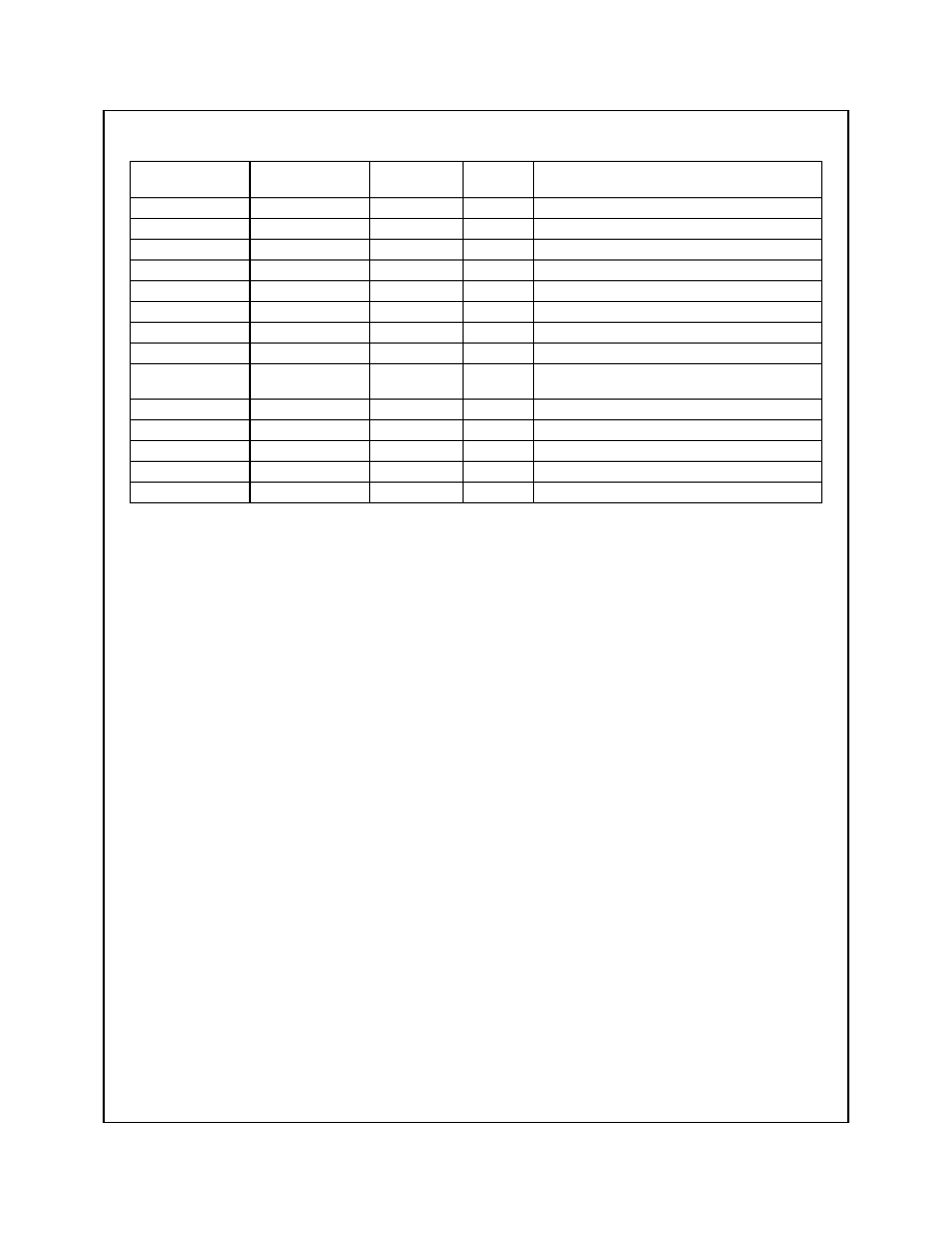
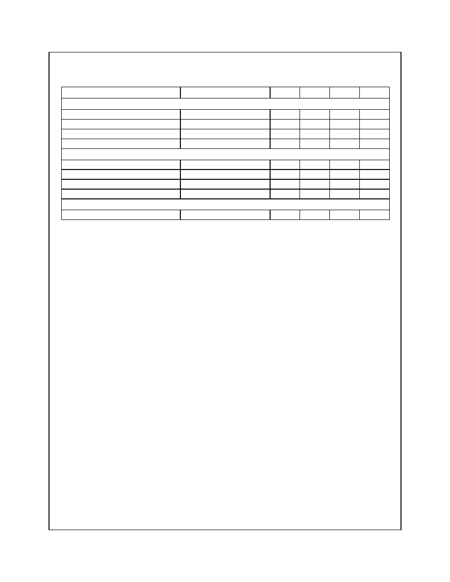
Absolute Maximum Ratings (Ta = 25
∞
C)
NOTE
:
Parameter
Value
Unit
Supply Voltage (Signal block)
7
V
Supply Voltage (Digital block)
7
V
Supply Voltage (Spindle/Sled/BTL/BTL pre driver)
15
V
Power
D
issipation (56-TSSOP-EP)
1.6 / 3.2 / 4.1
W
Power
D
issipation (56-SSOP-HS)
3.1 / 4.7
W
Operating Temperature Range
-20 to +75
∞
C
Storage
T
emperature Range
-40
to +150
∞
C
Maximum Output Current (Spindle)
2.0
A
Maximum Output Current (CH1/2/3/4, Sled)
1.0
A
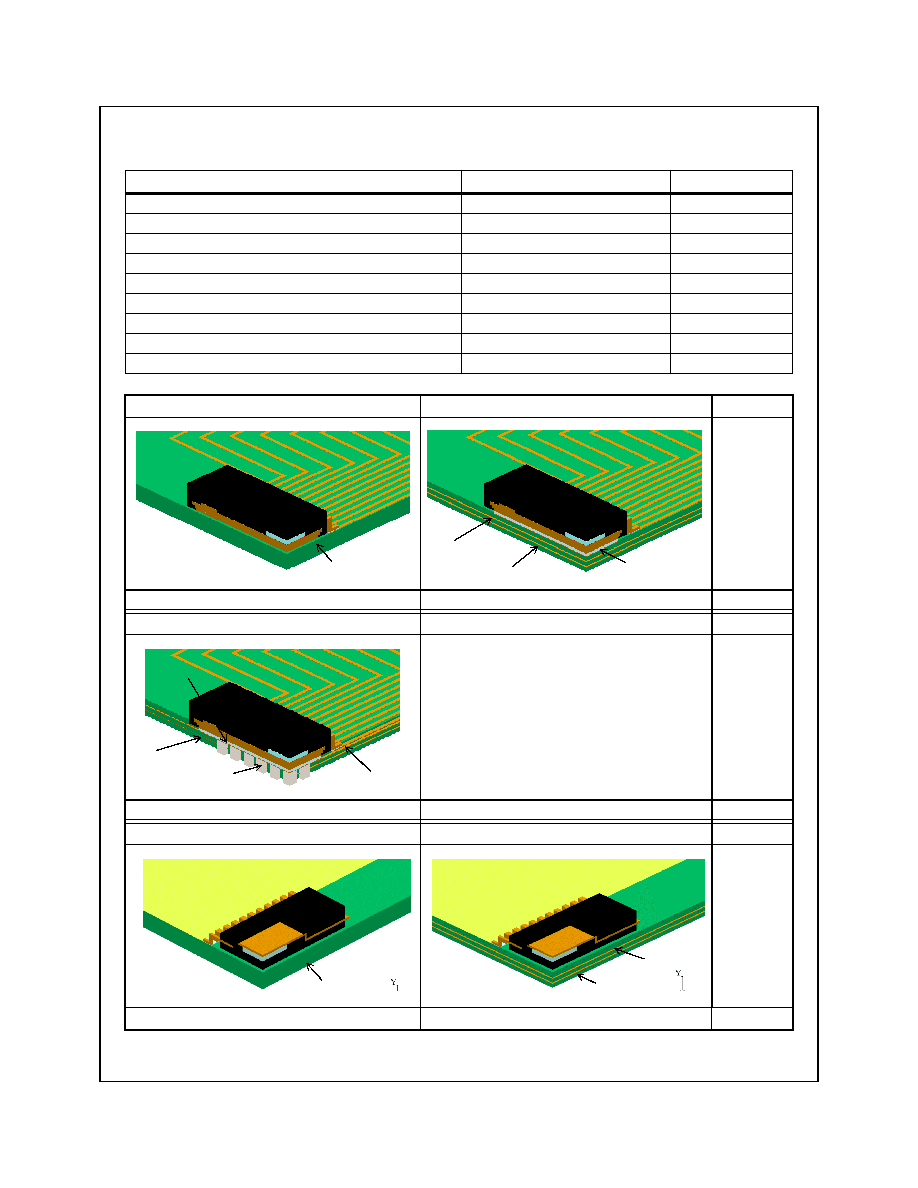
56-TSSOP-EP, Case 1
56-TSSOP-EP, Case 2
Remark
Pd is mea-
sured base on
the JEDEC/
STD(JESD
51-2)
Pd=1.6 W
Pd=3.2 W
56-TSSOP-EP, Case 3
Pd=4.1 W
56-SSOP-HS, Case 1
56-SSOP-HS, Case 2
Pd=3.1W
Pd=4.7W
soldering
Power plane(Cu)
VIA hole
GND plane(Cu)
Power plane(Cu)
soldering
PCB(glass-epoxy)
Power
plane(Cu)
GND plane(Cu)
PCB(glass-epoxy)
GND plane(Cu)
8
www.fairchildsemi.com
FAN8741/FAN8742 Rev. 1.0.1
F
A
N
8741
/F
A
N
8
742
S
p
indl
e mot
o
r
and 6-
CH act
uator dri
ver
1. 56-TSSOP-EP, Case 1: Single layer PCB with 1 signal plane only, PCB size is 76mm
◊
114mm
◊
1.6mm.
2. 56-TSSOP-EP, Case 2: Multi layer PCB with 1 signal, 1 power and 1 ground planes, PCB size is 76mm
◊
114mm
◊
1.6mm, Cu
plane sizes for power and ground is 74mm
◊
62mm
◊
0.035mm. Down pad of IC is soldered on the PCB.
3. 56-TSSOP-EP, Case 3: PCB condition is same to case 2 except via holes, which penetrate PCB all layers. Down pad of IC is sol-
dered on the PCB.
4. 56-SSOP-HS, Case 1: Single layer PCB with 1 signal plane only, PCB size is 76mm
◊
114mm
◊
1.6mm.
5. 56-SSOP-HS, Case 2: Multi layer PCB with 1 signal, 1 power and 1 ground planes, PCB size is 76mm
◊
114mm
◊
1.6mm, Cu
plane sizes for power and ground is 74mm
◊
62mm
◊
0.035mm.
6. Power dissipation is reduced by -12.8mW/
∞
C for using above Ta=25
∞
C in 56-TSSOP-EP, case 1.
7. Power dissipation is reduced by -25.6mW/
∞
C for using above Ta=25
∞
C in 56-TSSOP-EP, case 2.
8. Power dissipation is reduced by -32.8mW/
∞
C for using above Ta=25
∞
C in 56-TSSOP-EP, case 3.
9. Power dissipation is reduced by -24.8mW/
∞
C for using above Ta=25
∞
C in 56-SSOP-HS, case 1.
10. Power dissipation is reduced by -37.6mW/
∞
C for using above Ta=25
∞
C in 56-SSOP-HS, case 2.
11. Do not exceed P
D
and SOA (Safe Operating Area).
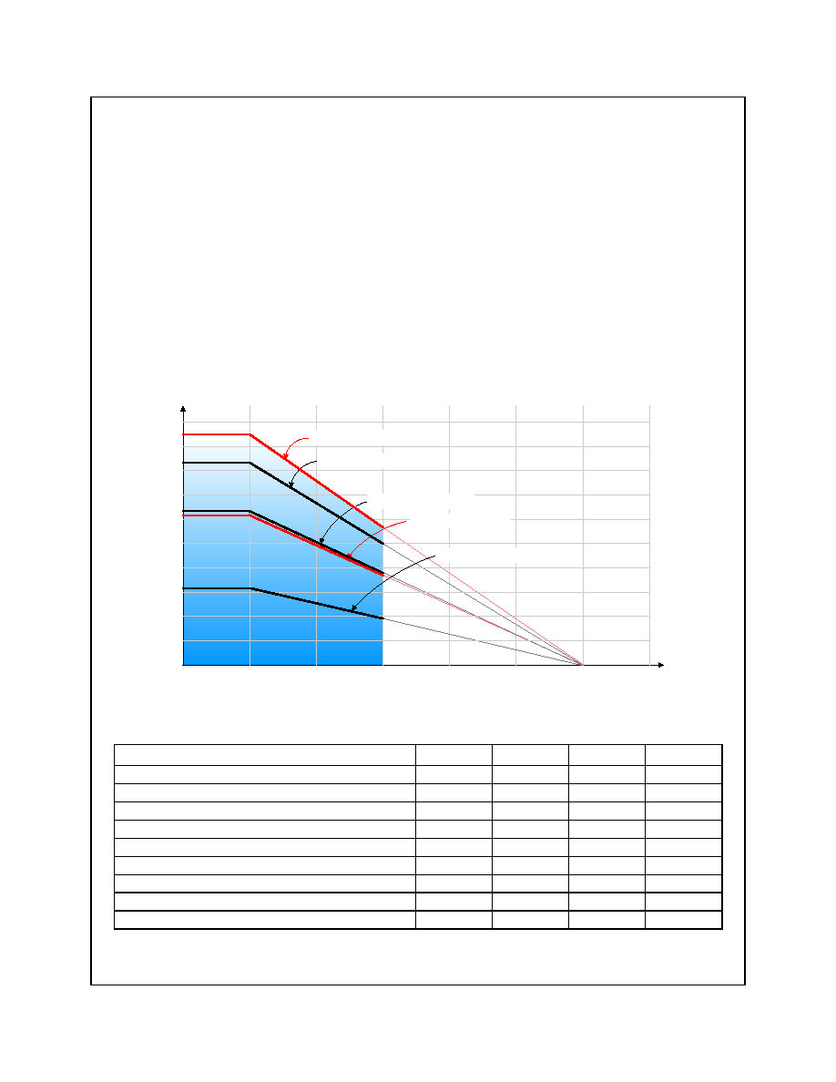
Power Dissipation Curve
Recommended Operating Conditions (Ta = 25
∞
C)
Parameter
Min.
Typ.
Max.
Unit
Supply Voltage (Spindle Signal block)
4.5
5
5.5
V
Supply Voltage (Digital block)
4.5
5
5.5
V
Supply Voltage (Spindle driver)
4.5
12
13.2
V
Supply Voltage (Sled driver)
4.5
12
13.2
V
Supply Voltage (BTL driver)
4.5
12
SV
CC2
V
Supply Voltage (BTL signal block)
4.5
12
13.2
V
Output current(Spindle)
-
1.0
1.5
A
Output current(Focus, Tracking, Loading)
-
0.5
0.8
A
Output current(Sled)
-
0.5
0.8
A
25
50
75
100
125
150
175
1
2
3
4
5
Ambient temperature, [
o
C]
Power dissipation, [W]
SOA
56-SSOP-HS,case2
56-TSSOP-EP,case3
56-TSSOP-EP,case2
56-SSOP-HS,case1
56-TSSOP-EP,case1
9
www.fairchildsemi.com
FAN8741/FAN8742 Rev. 1.0.1
F
A
N
8741
/F
A
N
8
742
S
p
indl
e mot
o
r
and 6-
CH act
uator dri
ver
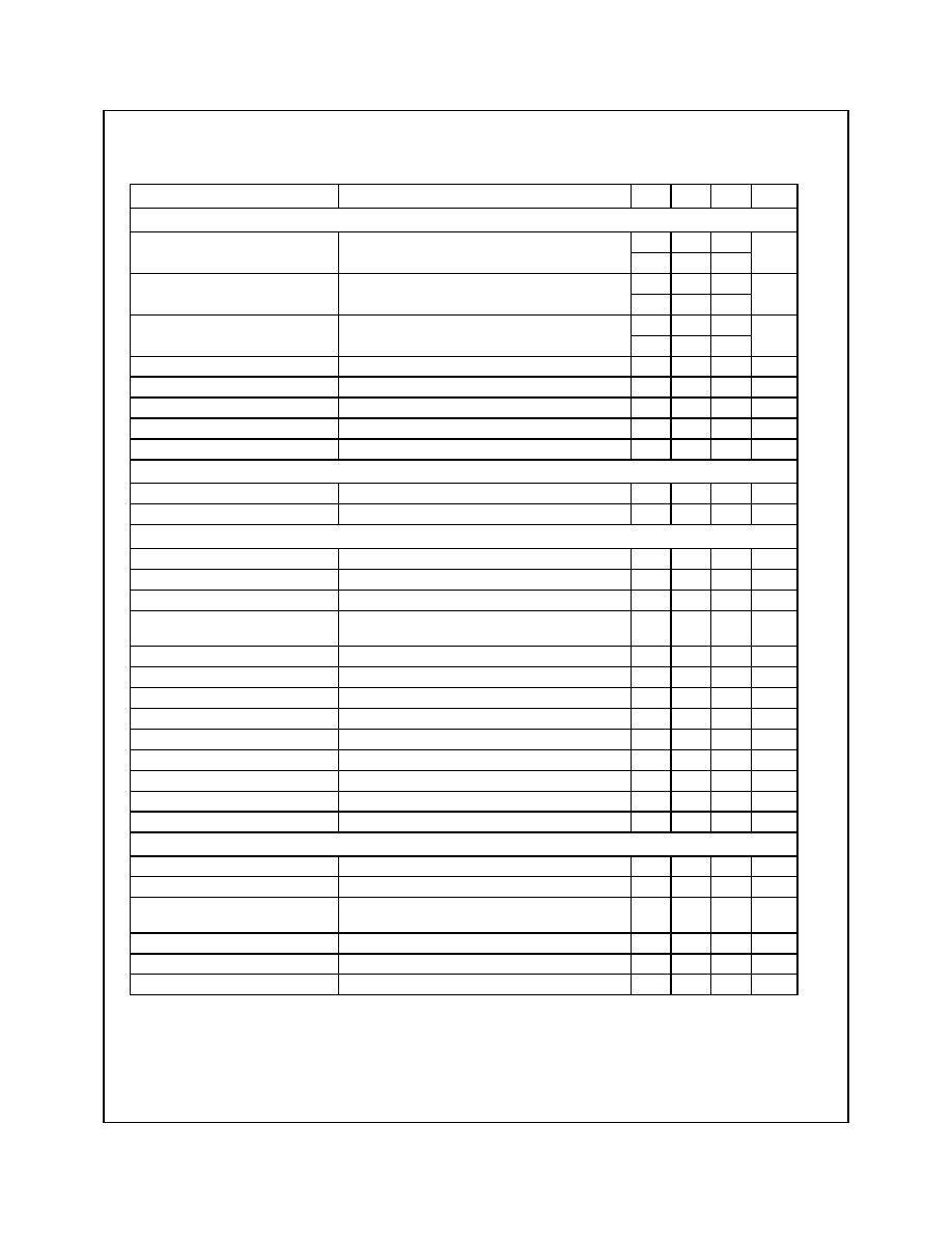
ELECTRICAL CHARACTERISTICS (Ta = 25
∞
c)
(Ta=25
∞
C, SVCC1=VDD=PVCC1=VM2=5V,VM1=SVCC2=PVCC2=PVCC3=12V unless otherwise noted)
* : Design guarantee specification
Parameter
Condition
Min. Typ. Max. Units
COMMON PART
Quiescent Circuit Current 1
Mute1=L, Mute2=L
-
1
-
mA
-
1
-
Quiescent Circuit Current 2
Mute1=L, Mute2=H
-
1.5
-
mA
-
9.5
-
Quiescent Circuit Current 3
Mute1=H, Mute2=H
-
4
-
mA
-
13
-
Mute Low Voltage
MUTE=variation
-
-
0.8
V
Mute High Voltage
MUTE=variation
3.0
-
-
V
Mute Input Current
MUTE=5V
-
130
-
µ
A
Charge Pump Voltage 1
I
PUMP
=0mA
-
19
-
V
Charge Pump Voltage 2
I
PUMP
=-1mA
-
18
-
V
THERMAL SHUTDOWN
Operating Temperature*
-
-
150
-
o
C
Hysteresis Temperature*
-
-
25
-
o
C
SPINDLE DRIVE PART
Control Input Deadzone11
SPIN>VREF
20
50
100
mV
Control Input Deadzone12
SPIN<VREF
-100
-50
-20
mV
Control Voltage Input Range
0
-
5
V
Output Gain
G
MSP
=G
VO
/RCS
SP
,
RCS
SP
=0.33
,
G
VO
=1[V/V]
2.55
3.0
3.45
A/V
Output On Resistance(upper)
Io=500mA
-
0.4
-
Output On Resistance(lower)
Io=500mA
-
0.4
-
Output Limit Current
RCS
SP
=0.33
-
1.5
-
A
Hall Amp Common Mode Input Range -
1
-
4
V
Minimum Hall Input Level*
-
50
-
-
mV
Hall Bias Output Voltage
I
HB
=10mA
0.5
1.0
1.5
V
Hall Bias Input Current
-
1
5
µ
A
FG Low Voltage
I
FG
=3mA
-
-
0.5
V
DIR Low Voltage
I
DIR
=3mA
-
-
0.5
V
SLED DRIVE PART
Control Input Deadzone21
SLIN1/SLIN2 > VREF
0
15
30
mV
Control Input Deadzone22
SLIN1/SLIN2 < VREF
-30
-15
0
mV
Output Gain
G
MSL
=G
VO
/RCS
SL
,
RCS
SL
=1
,
G
VO
=1[V/V]
0.85
1.0
1.15
A/V
Output On Resistance(upper)
Io=250mA
-
1.0
-
Output On Resistance(lower)
Io=250mA
-
1.0
-
Output Limit Current
RCS
SL
=1
-
0.5
-
A
10
www.fairchildsemi.com
FAN8741/FAN8742 Rev. 1.0.1
F
A
N
8741
/F
A
N
8
742
S
p
indl
e mot
o
r
and 6-
CH act
uator dri
ver
ELECTRICAL CHARACTERISTICS (Ta = 25
∞
C, continued)
(Ta=25
∞
C, SVCC1=VDD=PVCC1=VM2=5V,VM1=SVCC2=PVCC2=PVCC3=12V unless otherwise noted)
Parameter
Condition
Min.
Typ.
Max.
Units
CH1,CH2 DRIVE PART (TYPICALLY ACTUATOR DRIVER)
Output Saturation Voltage H
I
O
=500mA
0.5
V
Output Saturation Voltage L
I
O
=500mA
0.5
V
Closed Loop Voltage Gain
-
16.5
18
19.5
dB
Output Offset Voltage
VREF=IN1=IN2=1.65V
-50
-
50
mV
CH3,CH4 DRIVE PART (TYPICALLY TILT,LOADING DRIVER)
Output Saturation Voltage H
I
O
=500mA
1.0
V
Output Saturation Voltage L
I
O
=500mA
0.5
V
Closed Loop Voltage Gain
-
16.5
18
19.5
dB
Output Offset Voltage
VREF=IN3=IN4=1.65V
-50
-
50
mV
CH1,CH3 GAIN DIFFERENCE SPEC (TYPICALLY FOCUS,TILT DRIVER)
CH1-CH3 Gain Difference
G
VFT12
- G
VFT34
-0.5
0
0.5
dB
11
www.fairchildsemi.com
FAN8741/FAN8742 Rev. 1.0.1
F
A
N
8741
/F
A
N
8
742
S
p
indl
e mot
o
r
and 6-
CH act
uator dri
ver
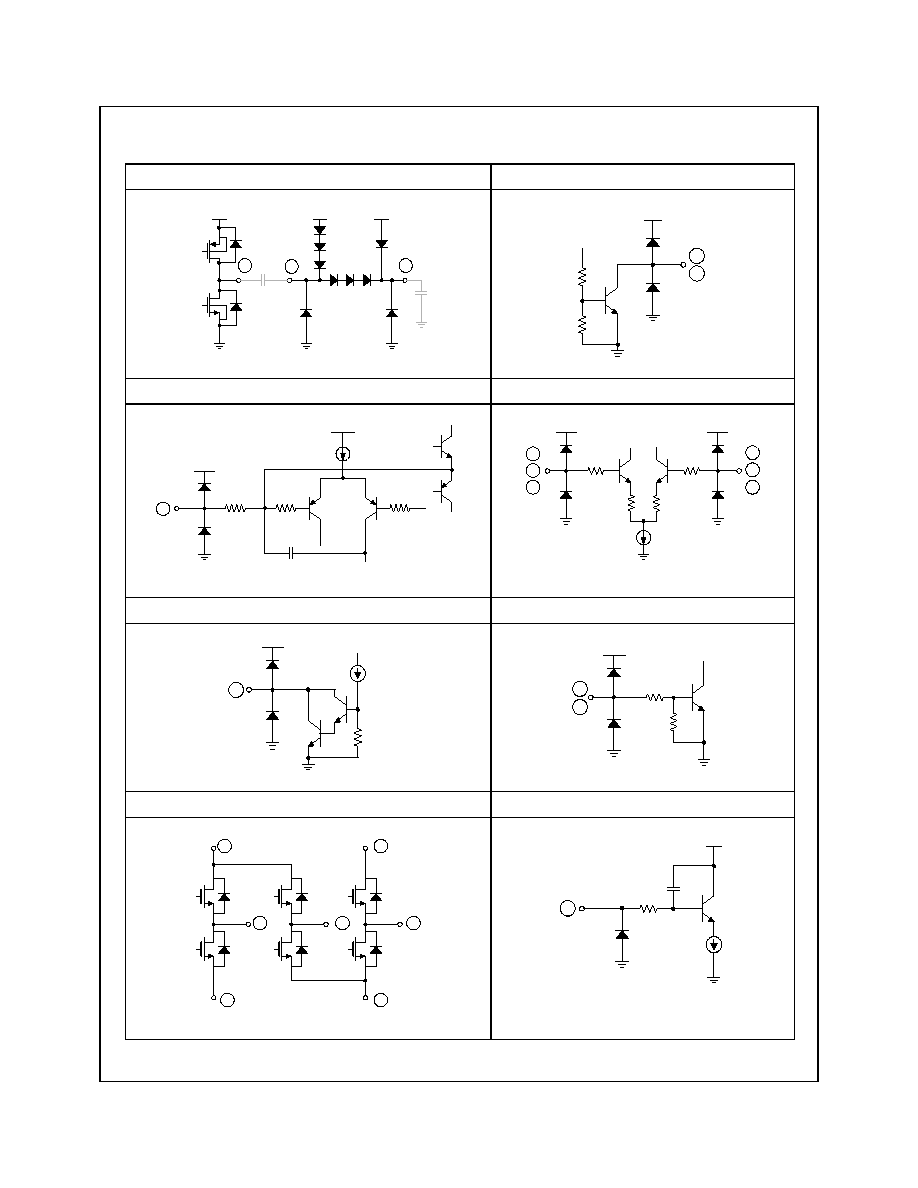
Equivalent Circuits
(Pins numbered according to FAN8741MTF)
Charge Pump Outputs
FG/DIR Outputs
Spin Input
Hall Inputs
Hall Bias Input
Mute1 & 2 Inputs
Spindle Drive Outputs
Spindle Current Sensing Input
53
SVCC2
SVCC2
55
SVCC2
54
SVCC1
50
51
10K
1K
1K
SVCC1
49
SVCC1
Ref
2
3
4
5
6
7
3K
SVCC1
3K
SVCC1
1K
1K
60K
SVCC1
8
40K
40K
22
23
SVCC2
14
15
13
12
10
11
9
15
VM1
12
www.fairchildsemi.com
FAN8741/FAN8742 Rev. 1.0.1
F
A
N
8741
/F
A
N
8
742
S
p
indl
e mot
o
r
and 6-
CH act
uator dri
ver
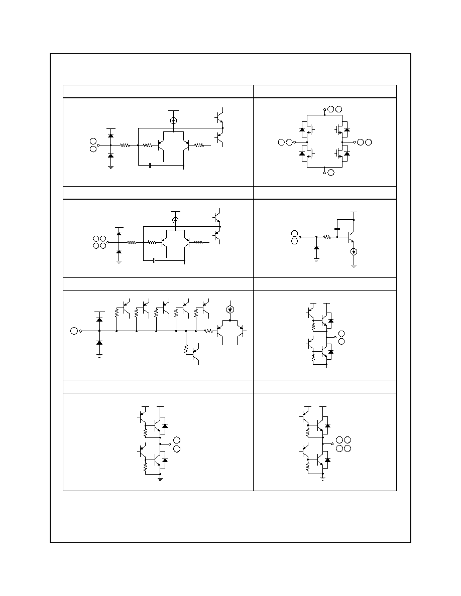
Equivalent Circuits(continued)
(Pins numbered according to FAN8741MTF)
Sled 1 & 2 Inputs
Sled Drive Outputs
CH1/2/3/4 (BTL Channels) Inputs
Sled 1 & 2 Current Sensing Inputs
Reference Input
CH4 Outputs
CH3 Outputs
CH1 & 2 Outputs
10K
1K
1K
SVCC2
29
SVCC2
Ref
30
24 25
16 18
17 19
20
10K
1K
1K
SVCC2
34
SVCC2
Ref
47
33
46
24
VM2
25
1K
SVCC2
21
43
44
SVCC2 PVCC3
40
41
SVCC2 PVCC2
36
38
SVCC2 PVCC1
37
39
13
www.fairchildsemi.com
FAN8741/FAN8742 Rev. 1.0.1
F
A
N
8741
/F
A
N
8
742
S
p
indl
e mot
o
r
and 6-
CH act
uator dri
ver
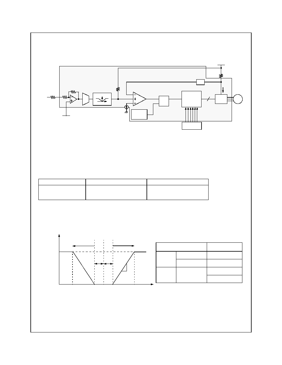
Application Information
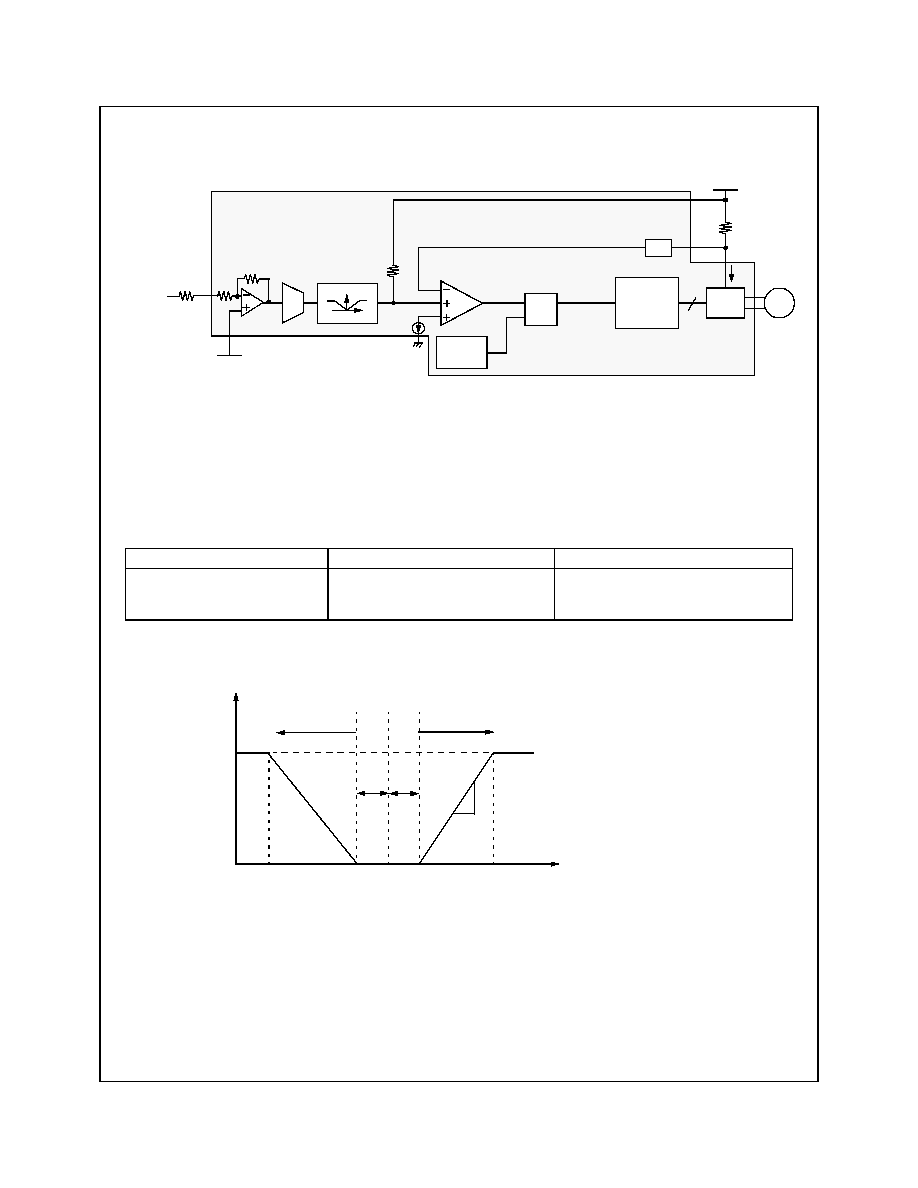
1. Torque Control & Output Current Control of 3-phase Bldc Motor
1) By amplifying the voltage difference between V
REF
and SPIN from Servo IC(or DSP), the Torque AMP produces the input
voltage(V
AMP
) which means input current command.
2) The output current (I
O
) is converted into the voltage (V
CS
) through the sense resistor (R
CS
) and compared with the V
AMP
.
3) The clock generator always make the RS latch become set periodically, this enables the output driver's on state, when the V
CS
and the V
AMP
are equal the state becomes off.
4) By the negative feedback loop, the sensed output voltage V
CS
equals to the V
AMP
.
5) Commuting sequence is selected by hall sensor input, and the minimum hall input is 50mV.
6) The gain and limit currents are calculated as shown in the table below.(Gvo=V
AMP
/(SPIN-V
REF
)=1[V/V]).
7) Spindle block adopts 180
o
commutation methodology which is fully compatible with a conventional BLDC spindle motor. Users
don't need to change or modify their spindle motor.
8) The range of the input voltage is as shown below when Rcs=0.33
, R
EXT1
=0.
Limit current
Input/Output gain[A/V]
Remark
is gain scaler
Torque AMP
V
REF
SPIN
Commutator
Driver
M
Rcs
Vcs
+
-
Io
V
AMP
+
-
LPF
R
S
Q
Clock
Generator
Hall sensor
R
EXT1
VM1
Inside IC
IOMAX
6
10K
10K
0.5
Rcs
-----------
10K
R
EXT1
10K
+
-------------------------------------------
G
VO
RCS
--------------
∑
10K
R
EXT1
10K
+
-------------------------------------------
Forward
Dead
Reverse
[A]
0
SPIN-V
REF
1.5
50mV
-50mV
zone-
G
MSP
=G
VO
/ R
CS
Dead
zone+
Current
Rotation
MUTE2
=H
SPIN
> V
REF
Forward rotation
SPIN
< V
REF
Reverse brake
MUTE2
=L,open
-
Short brake
Short brake
14
www.fairchildsemi.com
FAN8741/FAN8742 Rev. 1.0.1
F
A
N
8741
/F
A
N
8
742
S
p
indl
e mot
o
r
and 6-
CH act
uator dri
ver
2. Torque Control & Output Current Control Of Sled Motor(2-phase Step Motor)
1) By amplifying the voltage difference between V
REF
and SLIN1(or SLIN2) from Servo IC(or DSP), the Torque AMP produces
the input voltage(V
AMP
) which means input current command.
2) The output current (I
O
) is converted into the voltage (V
CS
) through the sense resistor (R
CS
) and compared with the V
AMP
.
3) The clock generator always make the RS latch become set periodically, this enables the output driver's on state, when the V
CS
and the V
AMP
are equal the state becomes off.
4) By the negative feedback loop, the sensed output voltage V
CS
equals to the V
AMP
.
5) To avoid output upper and lower transistor's short through, a switch trick is needed. Turn on delay time is 1usec, so the phase
delay time,when changing the current direction, is 1usec.
6) The gain and limit currents are calculated as shown in the table below.(Gvo=V
AMP
/[SLIN1(or SLIN2)-V
REF
]=1[V/V]
7)
The range of the torque voltage is as shown below when Rcs=1W, R
EXT1
=0
.
Torque limit current
Input/Output gain[A/V]
Remark
is gain scaler
Torque AMP
SLIN1
Driver
M
Rcs
Vcs
+
-
Io
VM2
V
AMP
+
-
LPF
R
S
Q
Clock
Generator
Drive Logic
Inside IC
I
OMAX
4
(or SLIN2)
V
REF
R
EXT1
10K
10K
0.5
Rcs
-----------
10K
R
EXT1
10K
+
-------------------------------------------
G
VO
R
CS
--------------
∑
10K
R
EXT1
10K
+
-------------------------------------------
Forward
Dead
Reverse
[A]
0
SLIN1(or SLIN2)-V
REF
0.5
15mV
-15mV
zone-
G
MSL
=G
VO
/ R
CS
Dead
zone+
15
www.fairchildsemi.com
FAN8741/FAN8742 Rev. 1.0.1
F
A
N
8741
/F
A
N
8
742
S
p
indl
e mot
o
r
and 6-
CH act
uator dri
ver
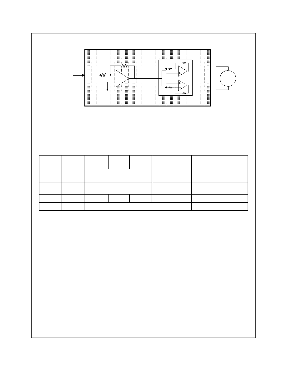
3. Channel 1~4 Schematic
∑ The reference voltage(ref) is given externally through pin21.
∑ The input OP-amp output signal is amplified by (20K/10K) times and then fed to the power amplifier. The gain of power amplifier is
4 so the total max gain of channels 1 through 4 is 8.
4. Mute Inputs
FAN8741 has 2 independent mute pins: Pin #22(MUTE1) and Pin #23(MUTE2). Details are shown below.
Note:
To make the spindle short brake, MUTE2 goes low and the spindle command must not be in deadzone(±50mV). When the spindle
command is within the deadzone, the spindle block enters disable mode even though MUTE2 is low.
MUTE1
MUTE2
SPIN-
DLE
SLED
CH1/2/3
CH4(typ. load-
ing driver)
SPINDLE brake type
H
H
Enable
Disable
Reverse brake when
SPIN<VREF
H
L
Enable
Disable
Short brake
SPIN
VREF
(note)
L
H
Disable
Enable
Disable
Enable
-
L
L
Disable
-
L
e
v
e
l sh
if
t
20k
10k
ref
power amp
M
Command
16
www.fairchildsemi.com
FAN8741/FAN8742 Rev. 1.0.1
F
A
N
8741
/F
A
N
8
742
S
p
indl
e mot
o
r
and 6-
CH act
uator dri
ver
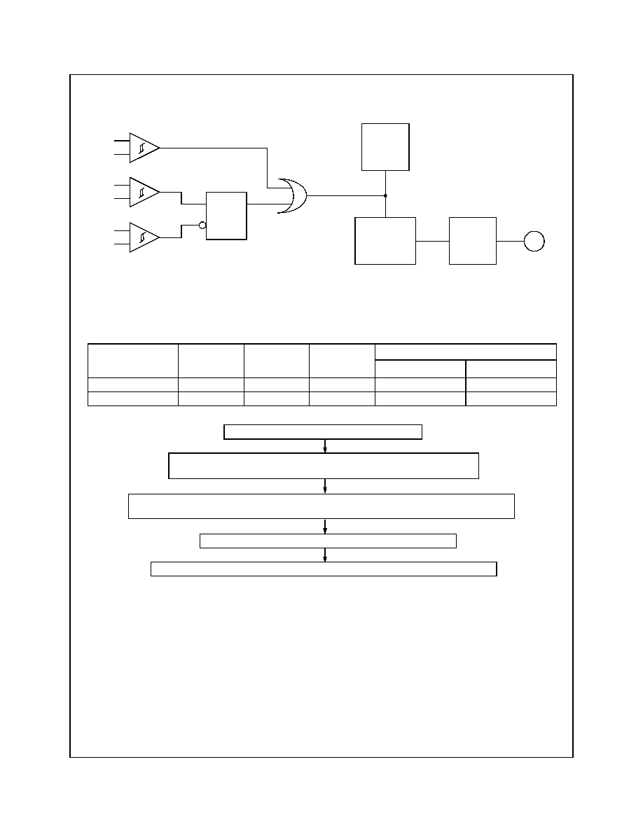
5. Reverse Rotation Prevention(Spindle)
1) As in the state of the forward rotation, the D-F/F output, Q is HIGH and the motor rotates normally. At this state, if the control
input is changed such that VREF>SPIN, then the motor rotates slowly by the reverse commutation in the driver. When the
motor begins to rotate in the reverse direction, the D-F/F output becomes Low and the OR Gate output becomes Low. This
prevents the motor from continuing to rotate in the reverse direction. This operation principle is shown in the following table
and flow chart.
Rotation
HV
HW
D-F/F
(Q)
Reverse Rotation Preventer
V
REF
<SPIN
V
REF
>SPIN
Forward
H
H
L
H
Forward
-
Reverse
L
H
L
L
-
Brake and Stop
+
-
+
-
+
-
Current
Sense
Amp
Gain
Controller
Driver
D-F/F
M
D
Q
CK
HW+
HW-
HV+
HV-
SPIN
VREF
A
Low Active
Forward rotation at VREF< SPIN
Rotating speed is decreased due to reverse torque at VREF>SPIN
At the moment that the motor rotates in reverse, the reverse rotation preventer makes
Motor rotates in reverse for short time due to motor inertia
and appropriate mute combination. (Motor still rotates forward)
the output power stage equal to the short brake which is lower ,and three power transistors are fully turned on.
Power stage remains in short brake scheme until forward rotation command is received.
17
www.fairchildsemi.com
FAN8741/FAN8742 Rev. 1.0.1
F
A
N
8741
/F
A
N
8
742
S
p
indl
e mot
o
r
and 6-
CH act
uator dri
ver
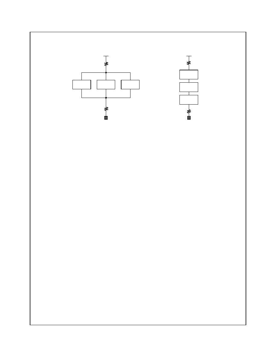
6. Hall Sensor Connection
7. PWM frequency
The PWM operation of the spindle and sled channels are controlled by an internal clock generator with a typical frequency of 100KHz.
8. ETC
1) FG and DIR output s are open-collector types.
2) By-pass capacitors are recommended at hall sensor and power supply inputs.
SVcc1
VH
HALL 1
HALL 2
HALL 3
VH
SVcc1
HALL 1
HALL 2
HALL 3
18
www.fairchildsemi.com
FAN8741/FAN8742 Rev. 1.0.1
F
A
N
8741
/F
A
N
8
742
S
p
indl
e mot
o
r
and 6-
CH act
uator dri
ver
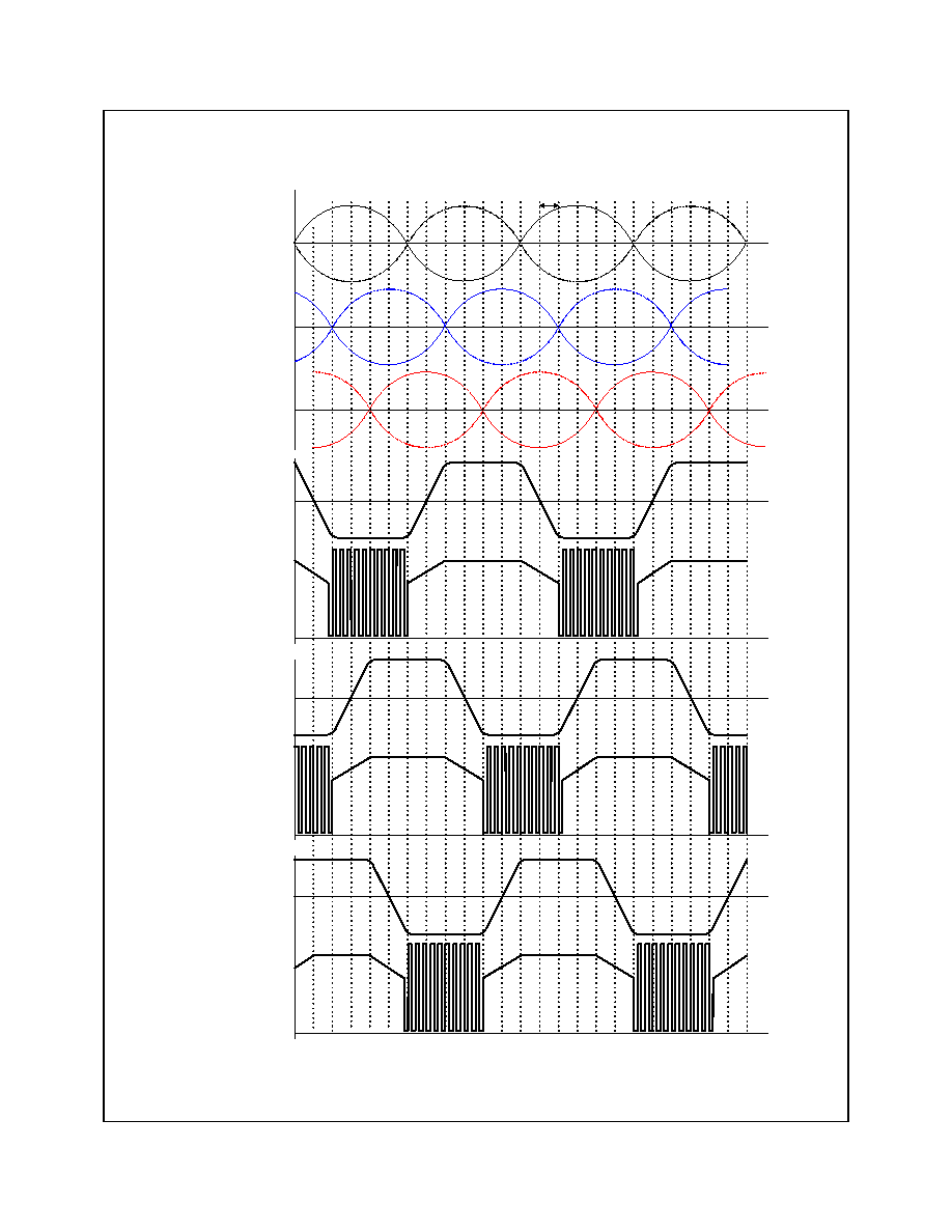
9. Spindle Part Input-output Timing Chart
30
o
HU
HV
HW
U current
(HU-)+(HV+)
U voltage
V current
(HV-)+(HW+)
V voltage
HU+
HU-
HV+
HV-
HW+
HW-
W current
(HW-)+(HU+)
W voltage
0[A]
0[V]
0[A]
0[V]
0[A]
0[V]
19
www.fairchildsemi.com
FAN8741/FAN8742 Rev. 1.0.1
F
A
N
8741
/F
A
N
8
742
S
p
indl
e mot
o
r
and 6-
CH act
uator dri
ver
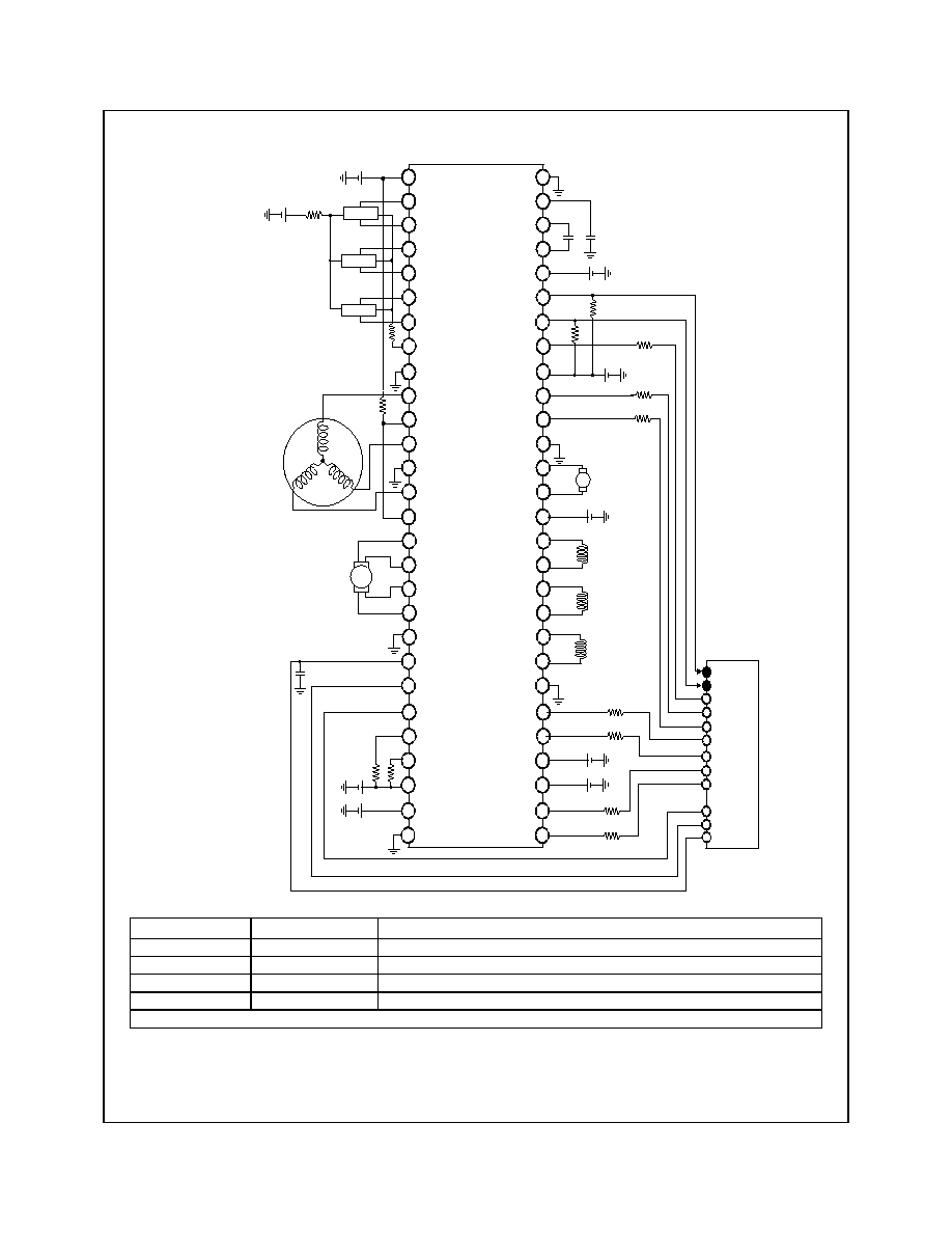
Typical Application Circuits(FAN8741MTF example)
Component
Reference value
Remark
R1~R7
10k
Gain scaling resistors. Please refer to pages 12,13, and 14.
R_hall1,R_hall2
100
Hall bias resistors
RSL1,RSL2
1
Rcs at sled driver. (I_limit=0.5A,Gain=0.5A/V@R6,R7 are 10k
)
RSP
0.33
Rcs at spindle driver. (I_limit=1.5A,Gain=1.5A/V@R1 is 10k
)
Bypass electrolytic capacitors(47~100
µ
F) are recommended at power supply inputs.
M
HALL-U
HALL-V
HALL-W
5V
3-Phase
BLDC Motor
Sled(stepping)
Motor
Focus
actuator
VM2
(for sled, 5~12V)
FAN
8
7
4
1
M
TF/
FA
N
8
7
42M
TF
(pad
do
wn
)
DO2
-
PVCC3
DO3
-
DO4+
IN4
IN3
VDD
SPIN
PGND5
DO4
-
48
47
46
45
44
43
42
41
40
39
38
37
36
35
DO3+
DIR
CP1
CP2
VCP
DGND
SVCC1
FG
56
55
54
53
52
51
50
49
DO1
-
34
33
32
31
DO2+
30
29
9
10
11
12
13
14
15
16
17
18
19
20
21
22
1
2
3
4
5
6
7
8
23
24
25
26
27
28
IN1
DO1+
PGND4
PVCC1
IN2
PVCC2
SLIN2
SLIN1
SL2+
RSP2
SL1+
W
RSP1
U
PGND1
VH
V
PGND2
SL1
-
HW
-
HV+
HU
-
HU+
VM1
HV
-
HW+
PGND3
SL2
-
MUTE2
REF
MUTE1
RSL2
RSL1
VM2
SGND
SVCC2
VM1
(for spindle,12V)
SVCC2(5~12V)
(SVCC2
!
!
!
!
PVCC1,2,3)
Tracking
actuator
Tilt actuator
M
Loading
motor
PVCC2(5~12V)
PVCC1(5~12V)
PVCC3(5~12V)
VDD (5V)
SVCC1(5V)
D
SP or
co
ntrol
l
e
r
10
k
(f
u
l
l
up
R)
10
k
(f
u
l
l
u
p
R)
0.1
µ
F
RSL1
RSL2
RSP
R_hall2
R_hall1
0.
1
µ
F
0.
1
µ
F
R1
R2
R3
R4
R5
R6
R7
20
www.fairchildsemi.com
FAN8741/FAN8742 Rev. 1.0.1
F
A
N
8741
/F
A
N
8
742
S
p
indl
e mot
o
r
and 6-
CH act
uator dri
ver
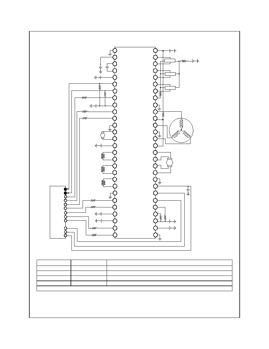
Typical Application Circuits(FAN8741G example)
Component
Reference value
Remark
R1~R7
10k
Gain scaling resistors. Please refer to 12,13,14 pages.
R_hall1,R_hall2
100
Hall bias resistors
RSL1,RSL2
1
Rcs at sled driver. (I_limit=0.5A,Gain=0.5A/V@R6,R7 are 10k
)
RSP
0.33
Rcs at spindle driver. (I_limit=1.5A,Gain=1.5A/V@R1 is 10k
)
Bypass electrolytic capacitors(47~100
µ
F) are recommended at power supply inputs.
M
HALL-U
HALL-V
HALL-W
5V
3-Phase
BLDC Motor
Sled(stepping)
Motor
Focus
actuator
VM2
(for sled, 5~12V)
FA
N8741
G/
FA
N8742G
DO2
-
PVCC3
DO3
-
DO4+
IN4
IN3
VDD
SPIN
PGND5
DO4
-
9
10
11
12
13
14
15
16
17
18
19
20
21
22
DO3+
DIR
CP1
CP2
VCP
DGND
SVCC1
FG
1
2
3
4
5
6
7
8
DO1
-
25
26
DO2+
27
28
48
47
46
45
44
43
42
41
40
39
38
37
36
35
56
55
54
53
52
51
50
49
34
33
32
31
30
29
IN1
DO1+
PGND4
PVCC1
IN2
PVCC2
SLIN2
SLIN1
SL2+
RSP2
SL1+
W
RSP1
U
PGND1
VH
V
PGND2
SL1
-
HW
-
HV+
HU
-
HU+
VM1
HV
-
HW+
PGND3
SL2
-
MUTE2
REF
MUTE1
RSL2
RSL1
VM2
SGND
SVCC2
VM1
(for spindle,12V)
SVCC2(5~12V)
(SVCC2
!
!
!
!
PVCC1,2,3)
Tracking
actuator
Tilt actuator
M
Loading
motor
PVCC2(5~12V)
PVCC1(5~12V)
PVCC3(5~12V)
VDD (5V)
SVCC1(5V)
DS
P or
con
t
r
o
l
l
er
10k
(
f
ul
l
up
R)
10k
(
f
ul
l
up R
)
0.1
µ
F
RSL1
RSL2
RSP
R_hall2
R_hall1
0.1
µ
F
0.1
µ
F
R1
R2
R3
R4
R5
R6
R7
23
24
21
www.fairchildsemi.com
FAN8741/FAN8742 Rev. 1.0.1
F
A
N
8741
/F
A
N
8
742
S
p
indl
e mot
o
r
and 6-
CH act
uator dri
ver
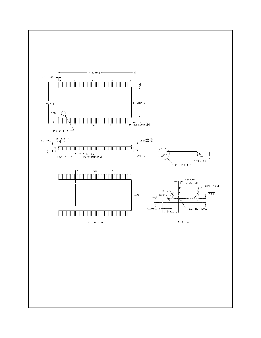
Package Dimensions of 56-TSSOP-EP
(lead frame is exposed to the bottom)
56-TSSOP-EP
unit=mm
22
www.fairchildsemi.com
FAN8741/FAN8742 Rev. 1.0.1
F
A
N
8741
/F
A
N
8
742
S
p
indl
e mot
o
r
and 6-
CH act
uator dri
ver
Package Dimensions of 56-SSOP-HS
(lead frame is exposed to the top)
56-SSOP-HS
unit=mm
23
www.fairchildsemi.com
FAN8741/FAN8742 Rev. 1.0.1
F
A
N
8741
/F
A
N
8
742
S
p
indl
e mot
o
r
and 6-
CH act
uator dri
ver