 | –≠–ª–µ–∫—Ç—Ä–æ–Ω–Ω—ã–π –∫–æ–º–ø–æ–Ω–µ–Ω—Ç: FAN8902 | –°–∫–∞—á–∞—Ç—å:  PDF PDF  ZIP ZIP |
©2002 Fairchild Semiconductor Corporation
www.fairchildsemi.com
Rev. 1.0.3
Features
∑ Built-in PWM Current Control Circuit
∑ Built-in 5V Regulator
∑ Low Supply Current
∑ Stalled Motor Current Limitation
∑ Built-in Over Voltage Protection (OVP)
∑ Built-in Over Current Protection (OCP)
∑ Built-in Load Dump Protection
∑ Built-in Thermal Shutdown (TSD) Circuit
∑ Built-in Under Voltage Lockout (UVLO) Circuit
Description
The FAN8902 is a monolithic integrated circuit, designed
for the PWM control of a DC fan motor current in an
automotive systems. It allows the fan motor speed to be
controlled linearly and efficiently.
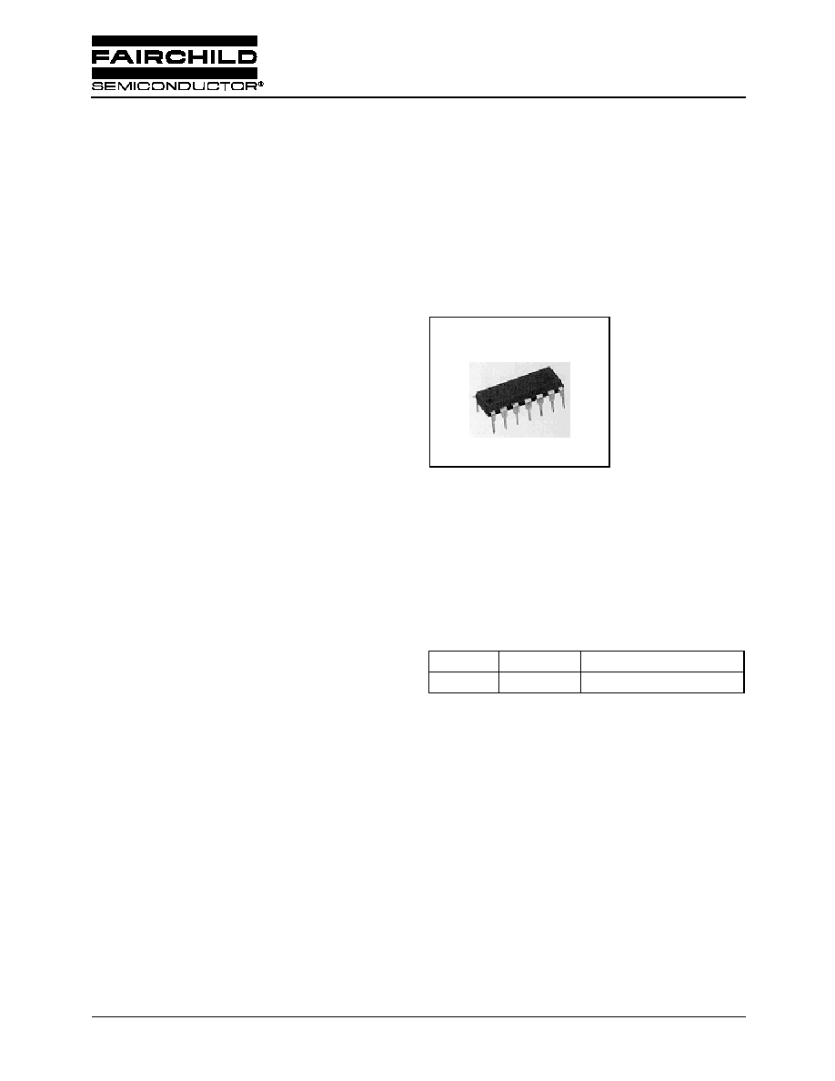
14-DIP-300
Typical Application
∑ DC for Motor Control for Automotive
Ordering Information
Device
Package
Operating Temperature
FAN8902
14-DIP-300
-40
∞
C ~ +90
∞
C
FAN8902(KA3902)
DC FAN Motor Controller
FAN8902(KA3902)
2
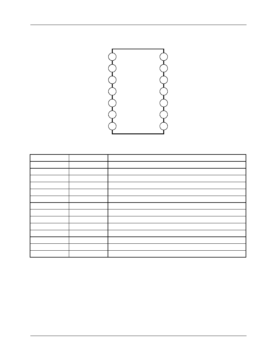
Pin Assignments
Pin Definitions
Pin Number
Pin Name
Pin Function Description
1
CMD
Motor Current Command Input
2
CMDa
Optional OP Amplifier Output
3
CMDb
Optional OP Amplifier (-) Input
4
SGND
Signal GND
5
R
T
/ C
T
Oscillator Time Constant
6
VREF
Voltage Reference (5V)
7
CH
Maximum Current Reference Input
8
NC
No Connection
9
CL
Minimum Current Reference Input
10
CS
Motor Current Sense Voltage Input
11
PGND
Power GND
12
OUT
Drive Output
13
V
CC
V
CC
14
La
Motor Current Maximum Reference Input
1
2
3
4
5
6
7
8
9
10
11
12
13
14
CMD
CMDa
CMDb
SG
R
T
/ C
T
VREF
CH
La
VCC
OUT
PG
CS
CL
NC
F A N 8 9 0 2
FAN8902(KA3902)
3
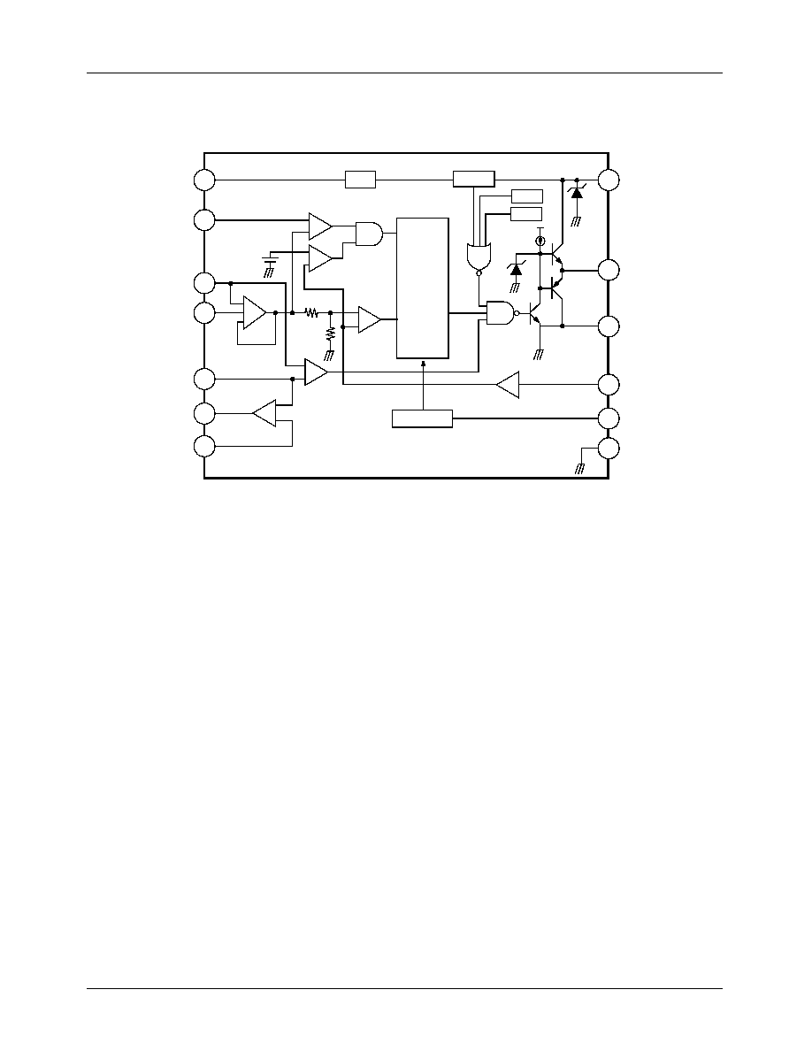
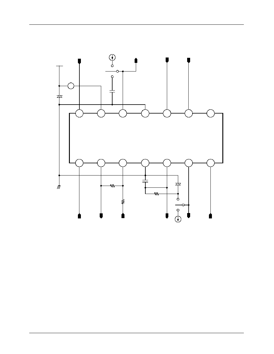
Internal Block Diagram
+
-
6
7
1
14
9
2
3
Vref
+
-
+
-
+
+
-
+
-
+
-
Oscillator
PWM
LOGIC
OVP
UVLO
TSD
PWM
Comparator
◊
5
1.3V
36V
4R
R
13
12
11
10
5
4
V
CC
OUT
PGND
CS
R
T
/C
T
SGND
Vref
CH
CMD
La
CL
CMDa
CMDb
FAN8902(KA3902)
4
Absolute Maximum Ratings
Operating Voltage
Temperature Characteristics
Parameter
Symbol
Value
Unit
Supply Voltage
V
CC
32
V
CMD Input Voltage
V
CMD
6
V
Peak Output Current
I
OPK
±
0.8
A
Power Dissipation
P
D
1
W
Parameter
Symbol
Min.
Typ.
Max
Unit
Power Supply Voltage
V
CC
9.0
12.0
32.0
V
Parameter
Symbol
Temp
Value
Unit
Vref Temperature Stability
V
ST
-40 ~ +90
∞
C
200
∞
C
Frequency Stability
F
ST
-40 ~ +90
∞
C
20 ~ 30
∞
C
Operating Temperature
T
OPR
-
-40 ~ +90
∞
C
Storage Temperature
T
STG
-
-60 ~ +150
∞
C
FAN8902(KA3902)
5
Electrical Characteristics
(Unless otherwise, Ta=25
∞
C, V
CC
=5V, V
M
=12V)
Parameter
Symbol
Conditions
Min.
Typ.
Max.
Unit
REFERENCE
Reference Voltage
Vref
Iref=1mA
4.75
5.0
5.25
V
Line Regulation
Vref1
V
CC
=9V ~ 32V
-
50
150
mV
Load Regulation
Vref2
Iref=1mA ~ 10mA
-
10
50
mV
UNDER VOLTAGE LOCKOUT (UVLO)
Start Threshold Voltage
V
TH(ST)
-
7.5
8.0
8.5
V
Threshold Hysteresis
V
HYS
-
1.0
1.2
1.4
V
PROTECTION
Over Voltage
O
VP
-
33
36
-
V
OSCILLATOR (R
T
=75k
, C
T
=1
n
F)
Frequency
fosc
-
20
25
30
kHz
Duty Cycle
Duty
-
90
95
-
%
CURRENT SENSING INPUT
Threshold Voltage
V
TH(ST)
V
CMD
= 5V
0.19
0.20
0.21
V
OUTPUT DRIVER
Output Voltage Switching Limit
V
OLIM
V
CC
= 18V, Cld =1nF
-
15
-
V
Low Output Voltage
V
OL1
Iout = 20mA
-
-
0.4
V
V
OL2
Iout = 200mA
-
-
2.2
V
High Output Voltage
V
OH1
Iout = -20mA
10.0
-
-
V
V
OH2
Iout = -200mA
9.0
-
-
V
Rising Time
Tr
Cld = 1nF
-
100
200
ns
Falling Time
Tf
Cld = 1nF
-
100
200
ns
TOTAL STANDBY CURRENT
Start-up Current
I
ST
V
CC
= 7V
-
1.0
1.5
mA
Operating Supply Current
I
CC
V
CC
= 9V
-
6.0
8.0
mA
FAN8902(KA3902)
6
Application Information
1. Under Voltage Lockout (UVLO)
2. Current Sensing Circuit
The peak current, I
M(MAX)
=V
S
/R
S
For example, if a required maximum current, I
M(MAX)
=20[A]
3. Thermal Shutdown (Tsd)
When the chip, temperature rises up to 150
∞
C, the thermal shutdown (TSD) circuit is activated and the output driver turn off,
and then turn on again at 125
∞
C.
T
H(ST)
T
HYS
8.0V
1.2V
13
Vref &
output driver
FAN8902
I
CC
6mA
1mA
6.8V
8V
V
TH(ST)
PWM
Logic
◊
5
Imax=1V
+
-
Current amplifier
FAN8902
PWM comparator
12
10
M
R5
V
BAT
I
M
R
S
V
S
R
S
1V 5
/
20A
---------------
10 m
[
]
=
=
FAN8902(KA3902)
7
4. Oscillator Component Selection
The oscillator timing components can be calculated as follows:
For example, if fosc = 25kHz and duty = 95%
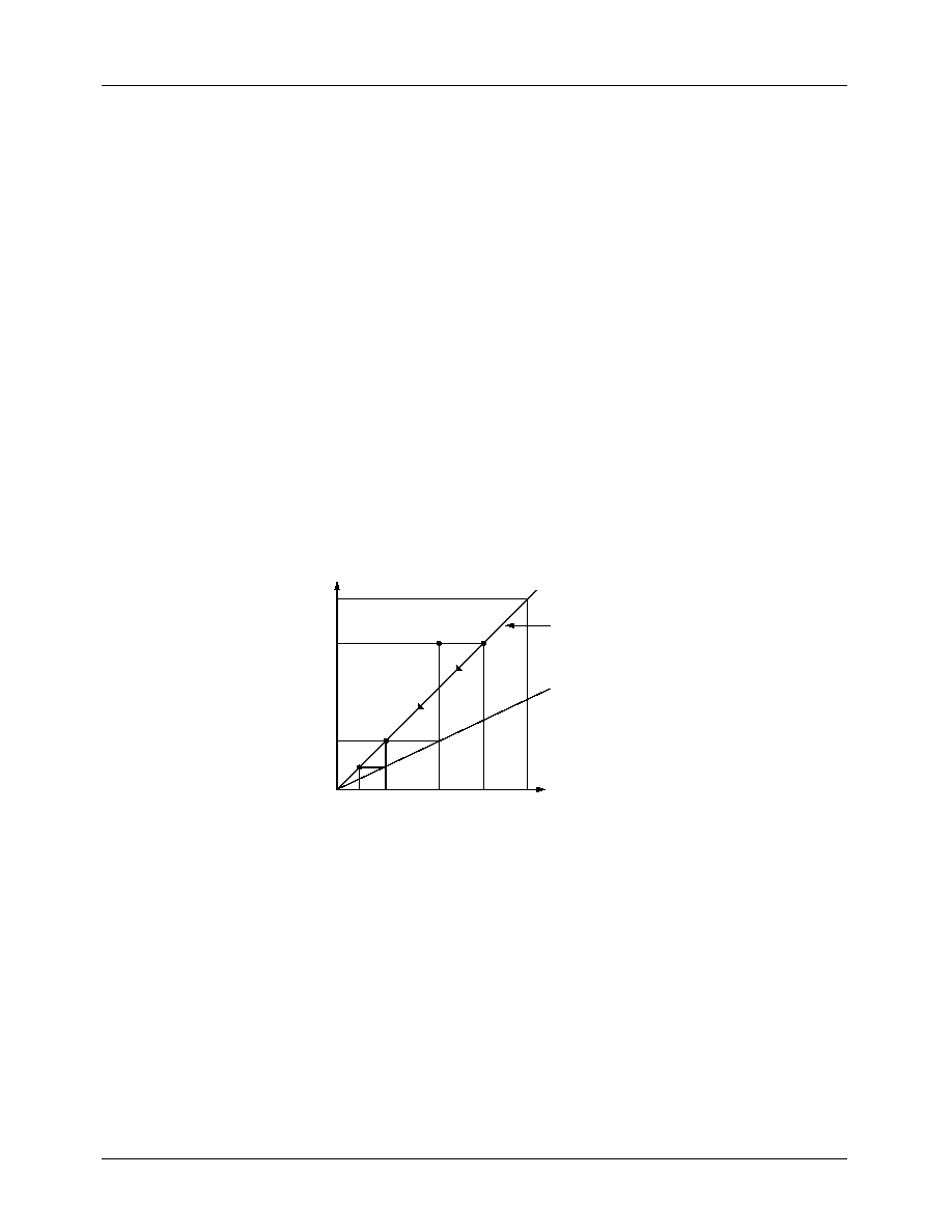
5. Current Command Input Section
The current command I* selects the lower value between V
CMD
and V
La
.
V
H
V
L
I
D
C
T
R
T
V/C
T
Vref
Logic
+
-
V
CT
[V]
V
H
=3.0
V
L
=1.75
T=40.0
T
C
=39.0
Td=1.0
t [
µ
s]
T
C
R
T
C
T
◊
In Vref V
L
≠
(
)
Vref V
H
≠
(
)
/
[
]
◊
=
T
D
C
T
V
H
V
L
≠
(
)
I
D
/
[
]
◊
=
fosc
1 T
C
T
D
+
(
)
/
=
1.875 R
T
C
T
◊
(
)
/
=
Duty
T
C
fosc
◊
100
◊
=
C
T
T
D
I
D
◊
(
)
V
H
V
L
≠
(
)
/
=
1000 pF
[
]
=
R
T
1.875 fosc C
T
◊
(
)
/
=
1.875 25kHz 1000pF
◊
(
)
/
=
75 k
[
]
=
+
-
+
-
+
14
1
CMD
V
CMD
La
V
La
4R
R
Logic
I*
FAN8902
FAN8902(KA3902)
8
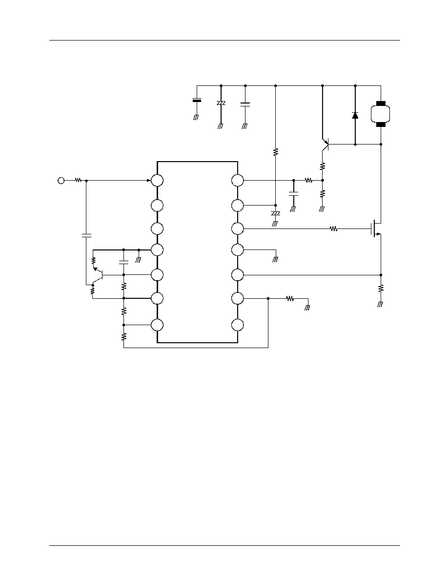
6. Slope Compensation
An unconditional instability of the inner current loop exists for any fixed frequency current-mode converter operating above
50% duty cycle. Therefore, to guarantee current loop stability, the slope of the compensation ramp must be greater than
one-half of the down slope of the current waveform. The ramp voltage for slope compensation is as follow,
7. Motor Stall Current Limitation
VRAMP
R14
R11
-----------
=
VOSC
◊
OSC
FAN8902
1
6
5
TR2
R11
C2
R12
R14
Vref
To PWM
Comparator
+
_
V
CMD
Slop Compensation
+
-
+
-
+
◊
5
1
14
10
12
M
VBAT
C1
C2
Q1
D1
IM
Q2
V
RS
R
S
R5
4R
R
V
CMD
R3
C4
R2
V
GS
R10
I*
Logic
PWM
COMP
Buffer-OP-amp
V
CS
V
LA
FAN8902
CMD
+
FAN8902(KA3902)
9
In the steady state, the terminal voltage on a motor is consisted of a back EMF and the voltage drop on the armarture resistors.
When the motor happens to be stalled, the back EMF becomes zero, and the motor current (I
M
) is quickly increased until a
maximum values.
Therefore the duty of the pin #12 output becomes lower because of the increase of the sense voltage (V
RS
). Also it makes the
voltage (V
La
) be lowered, then it makes the duty become lower again.
This mechanism makes the motor current hold very low value in the stalled motor state.
The voltage on pin #14 (V
La
) ia calculated as follows:
We can choose the ratio of the resistors, R2 and R3, as follows:
- Applied the rated voltage on motor, and then measured the current IRAT
- Matched the maximum command current, V
CMD,MAX
to I
RAT
.
V
CMD,MAX
= V
La,MAX
= R
S
◊
I
RAT
◊
5
◊
5
for example, if R
S
= 10m
and I
RAT
= 20[A] at V
BAT
= 13[V],
V
CMD,MAX
= V
La,MAX
= 10m
◊
20
◊
25 = 5V
- V
La,MAX
= 5V = V
BAT
◊
1
◊
R3 / (R2 + R3)
Ratio = R3 / (R2 + R3) = V
CMD,MAX
/ V
BAT
= 5 / 13
Therefore, R2 : R3 = 8 : 5
The buffer OP-amp selects the lower command between V
CMD
and V
La
so as to limit the stalled motor current to very low in
the above figure. Because of much larger V
La
than V
CMD
, the motor operating point stays at A. But the point gradually moves
toward B' and then B" through the curve from the instance of stall as the below figure.
V
La
V
BAT
D
◊
R3
R2 R3
+
----------------------
◊
=
Assumed the saturation voltage of Q1 is zero.
VLa curve
◊
(1 / R)
The voltage drop
on the amarture resistance
V
LA
V
CMD
I
RAT
V
MOTOR,STALL
V
BAT
V
LA
V
LA
V
MOTOR
Operating curve
A
B
B
'
B
"
FAN8902(KA3902)
10
8. Operational Mode Selection
The FAN8902 has three operation modes as follows:
- STOP: Turned-off the power MOSFET
- LINEAR: Linearly controlled the power MOSFET
- FULL-ON: Fully turned-on the power MOSFET
The voltage, V
SRT (PIN #9)
and V
MAX (PIN #7)
, in the application circuit are as follows:
- V
SRT (PIN #9)
= Vref
◊
R7 / (R5 + R6 + R7)
- V
MAX (PIN #7)
= Vref
◊
(R6 + R7) / (R5 + R6 + R7)
9. Over Voltage Protector (Ovp)
If the voltage, V
BAT
36[V], the output (pin #12) is grounded, and the switching device (power MOSFET) is turned-off, and
the motor is stopped. Then if the voltage, V
BAT
36[V], the switching device is turned-on again, and the motor is operated.
10. Totem-pole Output
The FAN8902 has a single totem-pole output driver which can be drive current to peak
±
0.8[A].
Motor current
Normal operation
Stalled state
Reduced switch-on time
V
CMD
V
CS
V
La
Uncontrolled without the FAN8902
Controlled with the FAN8902
I
MAX
current
[A]
I
SRT
V
SRT
V
CMD
[V]
V
MAX
V
BAT
FULL-ON
STOP
LINEAR
Motor
FAN8902(KA3902)
11
Test Circuit
1
2
3
4
5
6
7
8
9
10
11
12
13
14
R2
10k
R1
10k
R
T
75k
C2
+
22
µ
F
SW 1
C
T
1nF
IN 1
TP 1
IN 2
TP 2
Iout
TP 3
IN 3
IN 4
IN 5
IN 6
Iout
Cid
1
µ
F
C
O
47
µ
F
V
CC
SW 2
+
TP 4
A
F A N 8 9 0 2
CMD
CMDa
CMDb
SG
R
T
/ C
T
VREF
CH
La
VCC
OUT
PG
CS
CL
NC
FAN8902(KA3902)
12
Typical Application
1
2
3
4
5
6
7
8
9
10
12
11
13
14
M
NC
NC
Current
command
C
T
R
T
R5
R6
R7
NC
R
S
R4
C4
R3
R2
R10
R1
C3
+
+
V
BAT
Q1
D1
C1
C2
CMD
CMDa
CMDb
SG
R
T
/ C
T
VREF
CH
La
VCC
OUT
PG
CS
CL
NC
F A N 8 9 0 2
R14
R11
R12

FAN8902(KA3902)
13

FAN8902(KA3902)
9/17/02 0.0m 001
Stock#DSxxxxxxxx
2002 Fairchild Semiconductor Corporation
LIFE SUPPORT POLICY
FAIRCHILD'S PRODUCTS ARE NOT AUTHORIZED FOR USE AS CRITICAL COMPONENTS IN LIFE SUPPORT DEVICES
OR SYSTEMS WITHOUT THE EXPRESS WRITTEN APPROVAL OF THE PRESIDENT OF FAIRCHILD SEMICONDUCTOR
CORPORATION. As used herein:
1. Life support devices or systems are devices or systems
which, (a) are intended for surgical implant into the body,
or (b) support or sustain life, and (c) whose failure to
perform when properly used in accordance with
instructions for use provided in the labeling, can be
reasonably expected to result in a significant injury of the
user.
2. A critical component in any component of a life support
device or system whose failure to perform can be
reasonably expected to cause the failure of the life support
device or system, or to affect its safety or effectiveness.
www.fairchildsemi.com
DISCLAIMER
FAIRCHILD SEMICONDUCTOR RESERVES THE RIGHT TO MAKE CHANGES WITHOUT FURTHER NOTICE TO ANY
PRODUCTS HEREIN TO IMPROVE RELIABILITY, FUNCTION OR DESIGN. FAIRCHILD DOES NOT ASSUME ANY
LIABILITY ARISING OUT OF THE APPLICATION OR USE OF ANY PRODUCT OR CIRCUIT DESCRIBED HEREIN; NEITHER
DOES IT CONVEY ANY LICENSE UNDER ITS PATENT RIGHTS, NOR THE RIGHTS OF OTHERS.