 | ÐлекÑÑоннÑй компоненÑ: FDB4020P | СкаÑаÑÑ:  PDF PDF  ZIP ZIP |
Äîêóìåíòàöèÿ è îïèñàíèÿ www.docs.chipfind.ru
FDP4020P
FDP4020P Rev. A
FDP4020P/FDB4020P
P-Channel 2.5V Specified Enhancement Mode Field Effect Transistor
General Description
This P-Channel low threshold MOSFET has been
designed for use as a linear pass element for low voltage
outputs. In addition, the part may be used as a low voltage
load switch when switching outputs on or off for power
management.The part may also be used in conjunction
with DC-DC converters requiring P-Channel.
February 1999
PRELIMINARY
Features
· -16 A, -20 V. R
DS(on)
= 0.08
@ V
GS
= -4.5 V
R
DS(on)
= 0.11
@ V
GS
= -2.5 V.
· Critical DC electrical parameters specified at elevated
temperature.
· High density cell design for extremely low R
DS(on)
.
· TO-220 and TO-263 (D2PAK) package for both
through hole and surface mount applications.
· 175
°
C maximum junction temperature rating.
©
1999 Fairchild Semiconductor Corporation
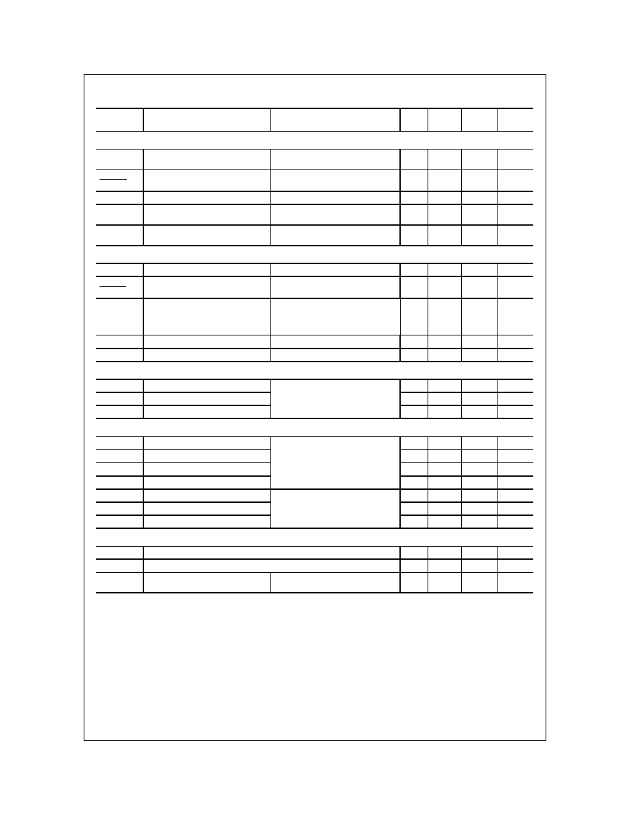
Absolute Maximum Ratings
T
A
= 25°C unless otherwise noted
Symbol
Parameter
FDP4020P
FDB4020P
Units
V
DSS
Drain-Source Voltage
-20
V
V
GSS
Gate-Source Voltage
±
8
V
I
D
Drain Current
- Continuous
-16
A
- Pulsed
-48
Total Power Dissipation @ T
C
= 25
°
C
37.5
W
P
D
Derate above 25
°
C
0.25
W/
°
C
T
J
, T
STG
Operating and Storage Junction Temperature Range
-65 to +175
°
C
Thermal Characteristics
R
JC
Thermal Resistance, Junction-to- Case
4
°
C/W
R
JA
Thermal Resistance, Junction-to- Ambient
(Note 1)
62.5
40
°
C/W
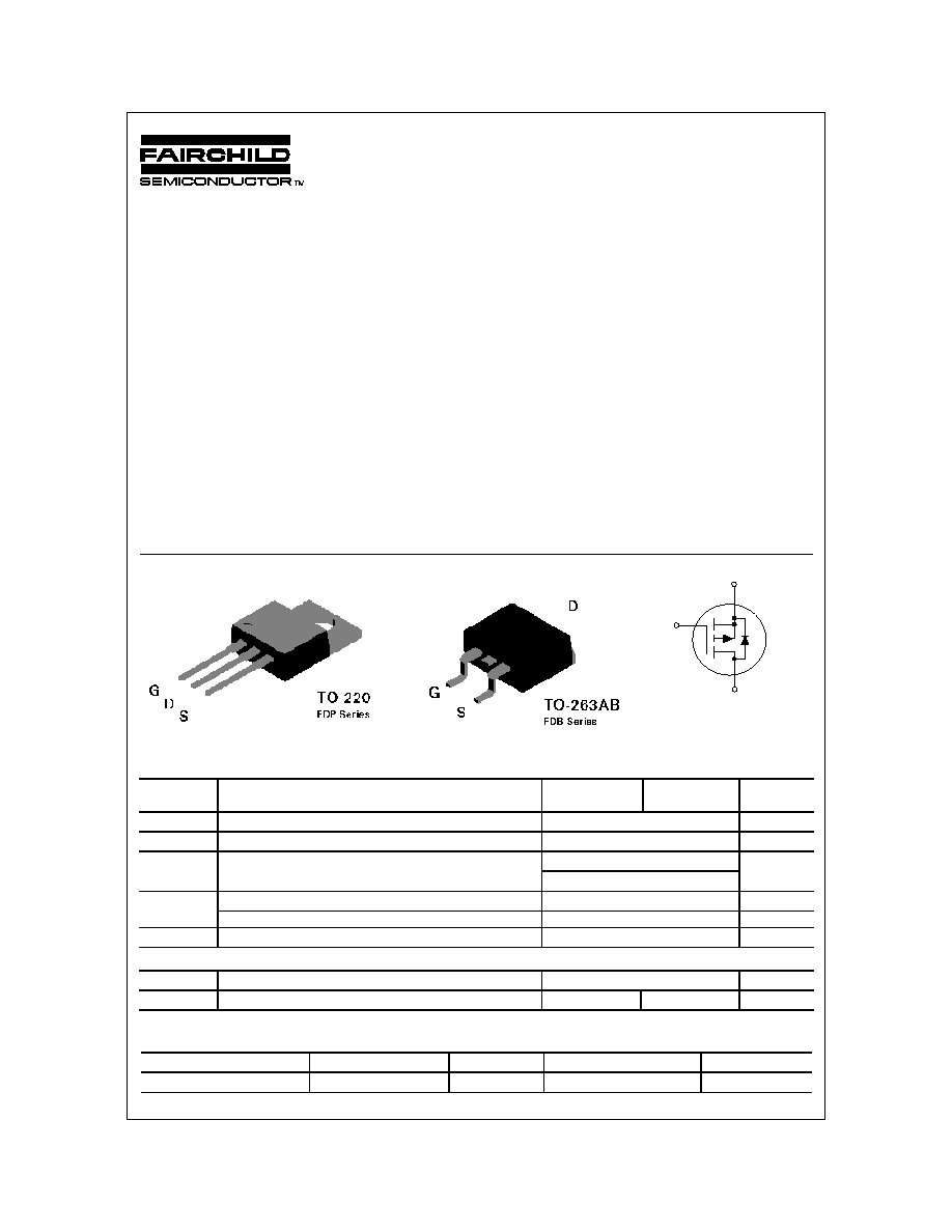
Package Outlines and Ordering Information
Device Marking
Device
Reel Size
Tape Width
Quantity
FDP4020P
FDP4020P
13''
12mm
2500 units
S
D
G
FDP4020P
FDP4020P Rev. A
Electrical Characteristics
T
A
= 25°C unless otherwise noted
Symbol
Parameter
Test Conditions
Min
Typ
Max
Units
Off Characteristics
BV
DSS
Drain-Source Breakdown
Voltage
V
GS
= 0 V, I
D
= -250
µ
A
-20
V
BV
DSS
T
J
Breakdown Voltage
Temperature Coefficient
I
D
= -250
µ
A, Referenced to 25
°
C
-28
mV/
°
C
I
DSS
Zero Gate Voltage Drain Current
V
DS
= -16 V, V
GS
= 0 V
-1
µ
A
I
GSSF
Gate-Body Leakage Current,
Forward
V
GS
= 8 V, V
DS
= 0 V
100
nA
I
GSSR
Gate-Body Leakage Current,
Reverse
V
GS
= -8 V, V
DS
= 0 V
-100
nA
On Characteristics
(Note 2)
V
GS(th)
Gate Threshold Voltage
V
DS
= V
GS
, I
D
= -250
µ
A
-0.4
-0.58
-1
V
V
GS(th)
T
J
Gate Threshold Voltage
Temperature Coefficient
I
D
= -250
µ
A, Referenced to 25
°
C
2
mV/
°
C
R
DS(on)
Static Drain-Source
On-Resistance
V
GS
= -4.5 V,I
D
= -8 A,
V
GS
= -4.5 V,I
D
= -8 A,T
J
=125
°
C
V
GS
= -2.5 V,I
D
= -7 A
0.068
0.098
0.096
0.08
0.13
0.110
I
D(on)
On-State Drain Current
V
GS
= -4.5 V, V
DS
= -5 V
-20
A
g
FS
Forward Transconductance
V
DS
= -5 V, I
D
= -8 A
14
S
Dynamic Characteristics
C
iss
Input Capacitance
665
pF
C
oss
Output Capacitance
270
pF
C
rss
Reverse Transfer Capacitance
V
DS
= -10 V, V
GS
= 0 V,
f = 1.0 MHz
70
pF
Switching Characteristics
(Note 2)
t
d(on)
Turn-On Delay Time
8
16
ns
t
r
Turn-On Rise Time
24
38
ns
t
d(off)
Turn-Off Delay Time
50
80
ns
t
f
Turn-Off Fall Time
V
DD
= -5 V, I
D
= -1 A,
V
GS
= -4.5 V, R
GEN
= 6
29
45
ns
Q
g
Total Gate Charge
9.5
13
nC
Q
gs
Gate-Source Charge
1.3
nC
Q
gd
Gate-Drain Charge
V
DS
= -5 V,
I
D
= -16 A, V
GS
= -4.5 V
2.2
nC
Drain-Source Diode Characteristics and Maximum Ratings
I
S
Maximum Continuous Drain-Source Diode Forward Current
(Note 2)
-16
A
I
SM
Maximum Pulsed Drain-Source Diode Forward Current
(Note 2)
-48
V
SD
Drain-Source Diode Forward
Voltage
V
GS
= 0 V, I
S
= -16 A
(Note 2)
-1.2
V
Notes:
1. R
JA
is the sum of the juntion-to-case and case-to-ambient thermal resistance.For T0-263 the device is mounted on circuit board with a 1in
2
pad
of 2 oz. copper.
2. Pulse Test: Pulse Width
300
µ
s, Duty Cycle
2.0%
FDP4020P
FDP4020P Rev. A
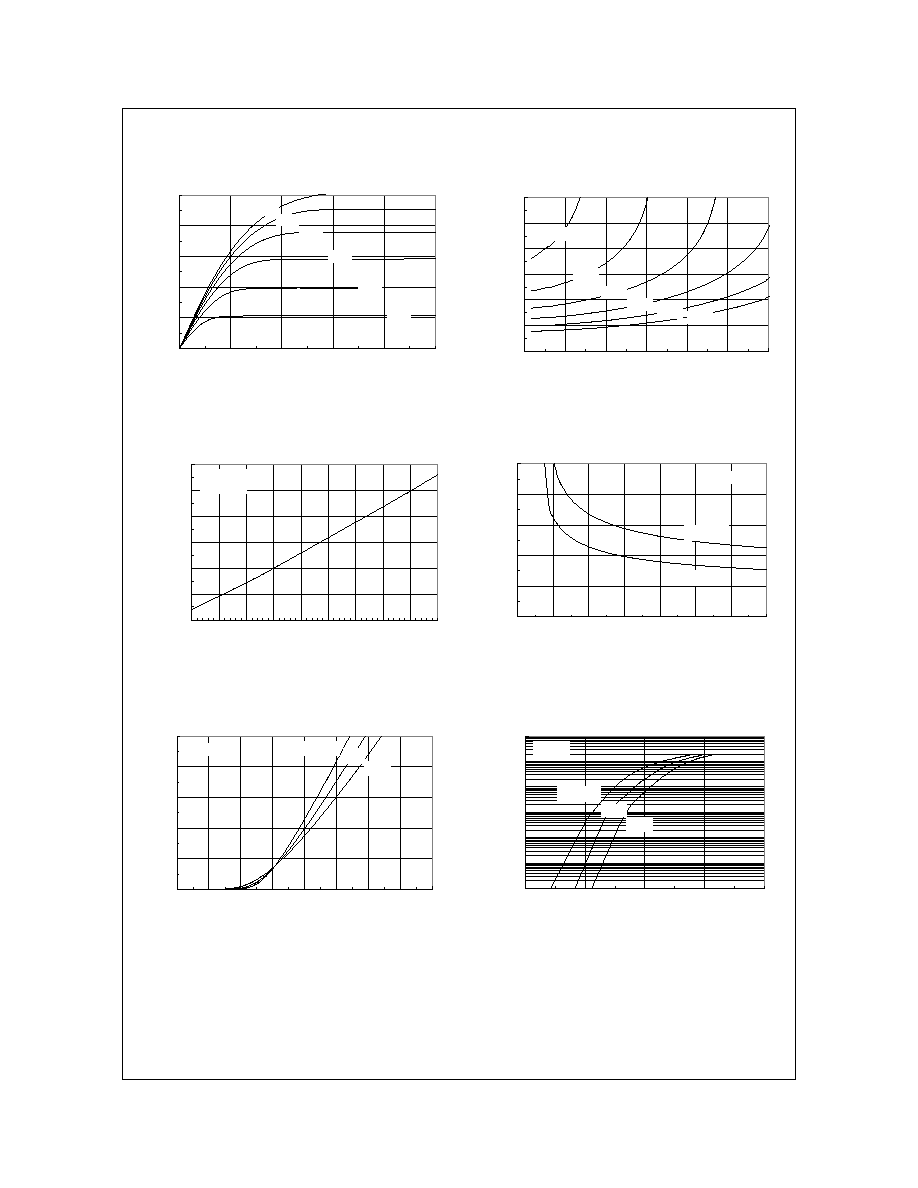
Typical Characteristics
Figure 1. On-Region Characteristics.
Figure 2. On-Resistance Variation
with Drain Current and Gate Voltage.
Figure 3. On-Resistance Variation
with Temperature.
Figure 4. On-Resistance Variation
with Gate-to-Source Voltage.
Figure 5. Transfer Characteristics.
Figure 6. Body Diode Forward Voltage
Variation with Source Current
and Temperature.
0
8
16
24
32
40
0
2
4
6
8
10
-V
DS
, DRAIN-SOURCE VOLTAGE (V)
-I
D
,
DRAI
N CURRE
NT
(A)
-2.0V
-2.5V
-3.0V
-3.5V
V
GS
= -4.5V
-4.0V
0.8
1
1.2
1.4
1.6
1.8
2
0
5
10
15
20
25
30
-I
D
, DIRAIN CURRENT (A)
R
D
S(O
N
)
,
NO
RM
ALI
ZE
D
DRA
IN-
S
O
URC
E
O
N
-
R
E
S
I
S
T
ANCE
V
GS
= -2.0V
-2.5V
-3.0V
-3.5V
-4.0V
-4.5V
0
4
8
12
16
20
0
0.5
1
1.5
2
2.5
3
3.5
4
-V
GS
, GATE TO SOURCE VOLTAGE (V)
-I
D
,
DRA
IN
CURRE
NT
(
A
)
T
A
= -55
o
C
25
o
C
125
o
C
V
DS
= -5V
0.0001
0.01
1
100
0
0.4
0.8
1.2
1.6
-V
SD
,
BODY DIODE FORWARD VOLTAGE (V)
-I
S
, RE
V
E
RS
E
DRAIN
CURRE
NT (
A
)
V
GS
= 0V
T
A
= 125
o
C
25
o
C
-55
o
C
0
0.04
0.08
0.12
0.16
0.2
1.5
2
2.5
3
3.5
4
4.5
5
-V
GS
, GATE TO SOURCE VOLTAGE (V)
R
D
S(O
N
)
,
ON
-R
ESI
S
T
A
N
C
E
(OH
M
)
I
D
= -8A
T
A
= 125
o
C
T
A
= 25
o
C
0.6
0.8
1
1.2
1.4
1.6
1.8
-50
-25
0
25
50
75
100
125
150
175
T
J
, JUNCTION TEMPERATURE (
o
C)
R
DS(ON)
, NORMALIZED
DRAIN-SOURCE ON-RESISTANCE
I
D
= -16A
V
GS
= -4.5V
FDP4020P
FDP4020P Rev. A
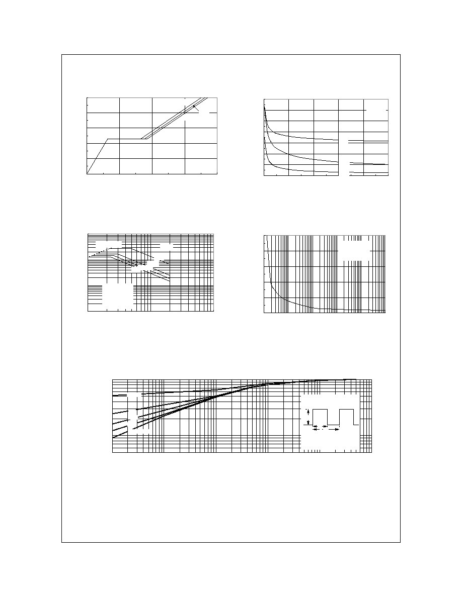
Typical Characteristics
(continued)
Figure 7. Gate-Charge Characteristics.
Figure 8. Capacitance Characteristics.
Figure 9. Maximum Safe Operating Area.
Figure 10. Single Pulse Maximum
Power Dissipation.
Figure 11. Transient Thermal Response Curve.
Thermal characterization performed using the conditions described in Note 1.
Transient themal response will change depending on the circuit board design.
0
200
400
600
800
1000
0.0001
0.001
0.01
0.1
1
10
SINGLE PULSE TIME (SEC)
POW
ER
(W
)
SINGLE PULSE
R
JC
= 4
o
C/W
T
A
= 25
o
C
0.1
1
10
100
1
10
100
-V
DS
, DRAIN-SOURCE VOLTAGE (V)
-I
D
, DRAIN CURRE
NT
(
A
)
R
DS(ON)
LIMIT
V
GS
= -4.5V
SINGLE PULSE
R
JC
= 4
o
C/W
T
A
= 25
o
C
DC 100ms
10ms
1ms
100
µ
s
0
200
400
600
800
1000
1200
1400
0
4
8
12
16
20
-V
DS
, DRAIN TO SOURCE VOLTAGE (V)
CAP
ACITA
NCE
(
p
F)
C
ISS
C
OSS
C
RSS
f = 1 MHz
V
GS
= 0 V
0.0001
0.001
0.01
0.1
1
10
0.05
0.1
0.2
0.5
1
t , TIME (sec)
T
R
A
N
SI
E
N
T
T
H
ER
MA
L
R
ESI
ST
A
N
C
E
1
Single Pulse
D = 0.5
0.1
0.05
0.2
r
(
t
)
, N
O
R
M
A
L
IZ
E
D
E
F
F
E
C
T
IV
E
Duty Cycle, D = t / t
1
2
R (t) = r(t) * R
R =
4°C/W
JC
JC
JC
T - T = P * R (t)
JC
A
J
P(pk)
t
1
t
2
0
1
2
3
4
5
0
3
6
9
12
Q
g
, GATE CHARGE (nC)
-V
GS
, GATE-SOURCE VOLTAGE (V)
I
D
= -16A
V
DS
= -5V
-10V
-15V
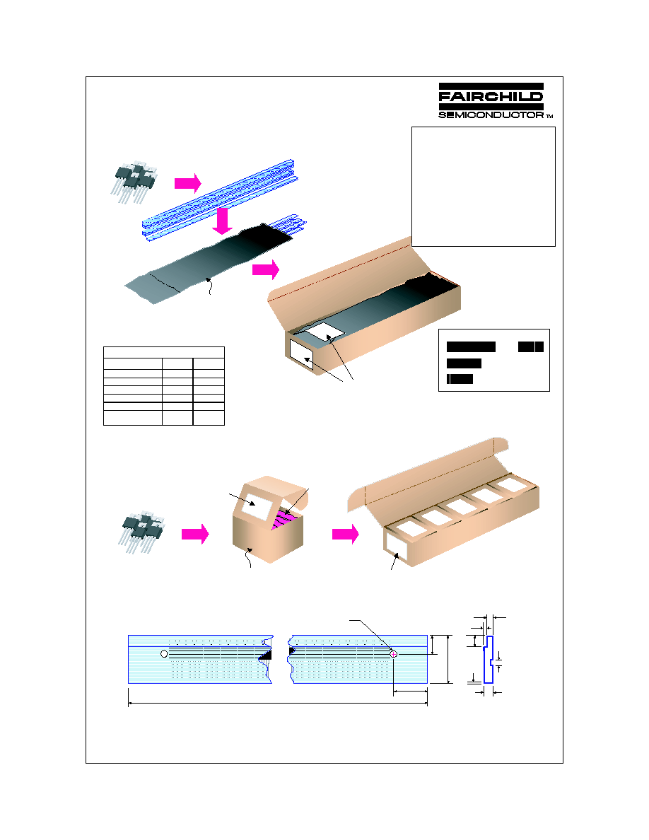
TO-220 Tape and Reel Data and Package Dimensions
August 1999, Rev. B
0.165
TO-220 Tube Packing
Configuration: Figur e 1.0
Note/Comments
Packaging Option
TO-220 Packaging Information
Standard
(no
f l ow code )
Packaging type
Rail/Tube
Qty per Tube/Box
45
Box Dimension (mm)
530x130x83
Max qty per Box
1,080
Weight per unit (gm)
1.4378
S62Z
BULK
300
114x102x51
1,500
1.4378
FSCINT Label
FSCINT Label
114mm x 102mm x 51mm
EO70 Immed iate Box
530mm x 130mm x 83mm
Intermediate bo x
300 units per
EO70 box
5 EO70 boxe s per per
Interm ediate Bo x
1500 uni ts maxi mum
qu ant it y per intermediate box
An ti-stati c
Bubbl e Sheet s
45 un it s per Tube
Conduct ive Plas ti c B ag
1080 uni ts maxi mum
qu ant it y per bo x
530mm x 130mm x 83mm
Intermediate bo x
FSCINT Label
12 Tube s per Bag
Note: All dim ensions are in inches
F9852
NDP4060L
F9852
NDP4060L
F9852
NDP4060L
F9852
NDP4060L
F9852
NDP4060L
F9852
NDP4060L
F9852
NDP4060L
F9852
NDP4060L
F9852
NDP4060L
F9852
NDP4060L
F9852
NDP4060L
F9852
NDP4060L
1.300
±
.015
0.080
0.032
±
.003
0.275
0.275
0.160
0.800
0.450
±
.030
20.000
+0.031
-0.065
0.123
+0.001
-0.003
LOT:
CBVK741B019
NSID:
FDP7060
D/C1:
D9842
SPEC REV:
B2
SPEC:
QTY:
1080
QA REV:
FAIRCHILD SEMICONDUCTOR CORPORATION
HTB:B
(FSCINT)
FSCINT Labe l samp le
TO-220 Tube
Configuration: Figure 4.0
TO-220 Packaging
Information: Figure 2.0
TO-220 bulk Packing
Configuration: Figure 3.0
2 bag s per Box
Packaging Description:
TO-220 parts are ship ped normally in tube. The tube is
made of PVC plastic treated with anti -stati c agent.These
tubes in standard option are placed inside a dissipative
plastic bag, barcode labeled, and placed inside a box
made of recyclable corrugated pa per. One box contains
two ba gs maximum (see fig. 1.0). And one or several o f
these boxes are placed inside a labeled shipp ing bo x
whic h c omes in different sizes dependi ng on the nu mber
of parts ship ped. The other option comes in bulk as
described in the Packagin g Information table. The unit s in
this option are placed inside a small box laid w ith anti-
static bubble sheet. These smaller boxes are individually
labeled and placed ins ide a larger box (see fig. 3.0).
These larger or intermediate boxes then will b e placed
finally inside a labeled shipping box whic h still comes in
different sizes depending on the number of units shipped.
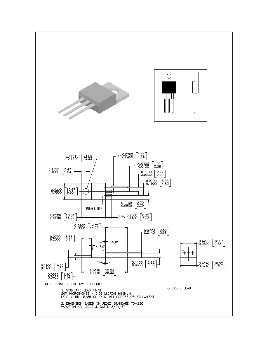
TO-220 (FS PKG Code 37)
TO-220 Tape and Reel Data and Package Dimensions, continued
September 1998, Rev. A
1:1
Scale 1:1 on letter size paper
Dimensions shown below are in:
inches [millimeters]
Part Weight per unit (gram): 1.4378

TRADEMARKS
ACExTM
CoolFETTM
CROSSVOLTTM
E
2
CMOS
TM
FACTTM
FACT Quiet SeriesTM
FAST
®
FASTrTM
GTOTM
HiSeCTM
The following are registered and unregistered trademarks Fairchild Semiconductor owns or is authorized to use and is
not intended to be an exhaustive list of all such trademarks.
LIFE SUPPORT POLICY
FAIRCHILD'S PRODUCTS ARE NOT AUTHORIZED FOR USE AS CRITICAL COMPONENTS IN LIFE SUPPORT
DEVICES OR SYSTEMS WITHOUT THE EXPRESS WRITTEN APPROVAL OF FAIRCHILD SEMICONDUCTOR CORPORATION.
As used herein:
1. Life support devices or systems are devices or
systems which, (a) are intended for surgical implant into
the body, or (b) support or sustain life, or (c) whose
failure to perform when properly used in accordance
with instructions for use provided in the labeling, can be
reasonably expected to result in significant injury to the
user.
2. A critical component is any component of a life
support device or system whose failure to perform can
be reasonably expected to cause the failure of the life
support device or system, or to affect its safety or
effectiveness.
PRODUCT STATUS DEFINITIONS
Definition of Terms
Datasheet Identification
Product Status
Definition
Advance Information
Preliminary
No Identification Needed
Obsolete
This datasheet contains the design specifications for
product development. Specifications may change in
any manner without notice.
This datasheet contains preliminary data, and
supplementary data will be published at a later date.
Fairchild Semiconductor reserves the right to make
changes at any time without notice in order to improve
design.
This datasheet contains final specifications. Fairchild
Semiconductor reserves the right to make changes at
any time without notice in order to improve design.
This datasheet contains specifications on a product
that has been discontinued by Fairchild semiconductor.
The datasheet is printed for reference information only.
Formative or
In Design
First Production
Full Production
Not In Production
DISCLAIMER
FAIRCHILD SEMICONDUCTOR RESERVES THE RIGHT TO MAKE CHANGES WITHOUT FURTHER
NOTICE TO ANY PRODUCTS HEREIN TO IMPROVE RELIABILITY, FUNCTION OR DESIGN. FAIRCHILD
DOES NOT ASSUME ANY LIABILITY ARISING OUT OF THE APPLICATION OR USE OF ANY PRODUCT
OR CIRCUIT DESCRIBED HEREIN; NEITHER DOES IT CONVEY ANY LICENSE UNDER ITS PATENT
RIGHTS, NOR THE RIGHTS OF OTHERS.
TinyLogicTM
UHCTM
VCXTM
ISOPLANARTM
MICROWIRETM
POPTM
PowerTrenchTM
QFETTM
QSTM
Quiet SeriesTM
SuperSOTTM-3
SuperSOTTM-6
SuperSOTTM-8