 | –≠–ª–µ–∫—Ç—Ä–æ–Ω–Ω—ã–π –∫–æ–º–ø–æ–Ω–µ–Ω—Ç: FDC6322 | –°–∫–∞—á–∞—Ç—å:  PDF PDF  ZIP ZIP |
November 1997
FDC6322C
Dual N & P Channel , Digital FET
General Description
Features
Absolute Maximum Ratings
T
A
= 25
o
C unless other wise noted
Symbol
Parameter
N-Channel
P-Channel
Units
V
DSS
, V
CC
Drain-Source Voltage, Power Supply Voltage
25
-25
V
V
GSS
, V
IN
Gate-Source Voltage,
8
-8
V
I
D
, I
O
Drain/Output Current
- Continuous
0.22
-0.46
A
- Pulsed
0.5
-1
P
D
Maximum Power Dissipation
(Note 1a)
0.9
W
(Note 1b)
0.7
T
J
,T
STG
Operating and Storage Tempature Ranger
-55 to 150
∞C
ESD
Electrostatic Discharge Rating MIL-STD-883D
Human Body Model (100pf / 1500 Ohm)
6
kV
THERMAL CHARACTERISTICS
R
JA
Thermal Resistance, Junction-to-Ambient
(Note 1a)
140
∞C/W
R
J
C
Thermal Resistance, Junction-to-Case
(Note 1)
60
∞C/W
FDC6322C.Rev B1
N-Ch 25 V, 0.22 A, R
DS(ON)
= 5
@ V
GS
= 2.7 V.
P-Ch 25 V, -0.46 A, R
DS(ON)
= 1.5
@ V
GS
= -2.7 V.
Very low level gate drive requirements allowing direct
operation in 3 V circuits. V
GS(th)
< 1.5 V.
Gate-Source Zener for ESD ruggedness.
>6kV Human Body Model
Replace NPN & PNP digital transistors.
These dual N & P Channel logic level enhancement mode field
effec transistors are produced using Fairchild's proprietary,
high cell density, DMOS technology. This very high density
process is especially tailored to minimize on-state resistance.
The device is an improved design especially for low voltage
applications as a replacement for bipolar digital transistors in
load switching applications. Since bias resistors are not
required, this dual digital FET can replace several digital
transistors with difference bias resistors.
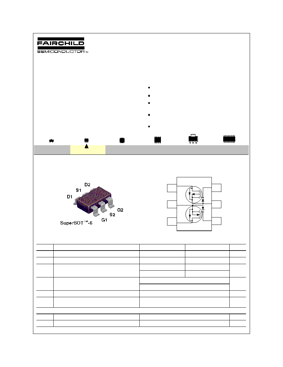
Mark: .322
SOT-23
SuperSOT
TM
-8
SOIC-16
SO-8
SOT-223
SuperSOT
TM
-6
1
5
3
2
6
4
© 1997 Fairchild Semiconductor Corporation
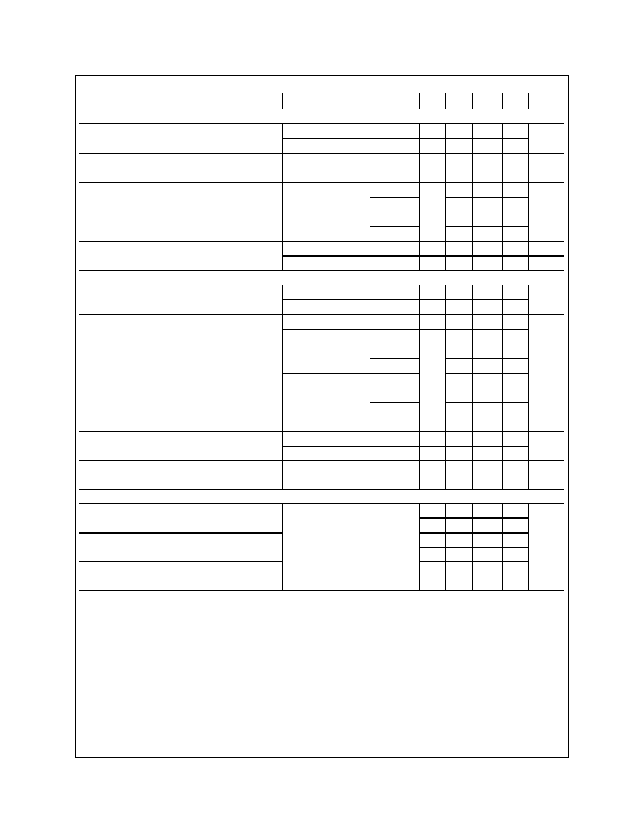
DMOS Electrical Characteristics
(
T
A
= 25
O
C unless otherwise noted )
Symbol
Parameter
Conditions
Type
Min
Typ
Max
Units
OFF CHARACTERISTICS
BV
DSS
Drain-Source Breakdown Voltage
V
GS
= 0 V, I
D
= 250 µA
N-Ch
25
V
V
GS
= 0 V, I
D
= -250 µA
P-Ch
-25
BV
DSS
/
T
J
Breakdown Voltage Temp. Coefficient
I
D
= 250 µA, Referenced to 25
o
C
N-Ch
25
mV /
o
C
I
D
= -250 µA, Referenced to 25
o
C
P-Ch
-22
I
DSS
Zero Gate Voltage Drain Current
V
DS
= 20 V, V
GS
= 0 V,
N-Ch
1
µA
T
J
= 55∞C
10
I
DSS
Zero Gate Voltage Drain Current
V
DS
=-20 V, V
GS
= 0 V,
P-Ch
-1
µA
T
J
= 55∞C
-10
I
GSS
Gate - Body Leakage Current
V
GS
= 8 V, V
DS
= 0 V
N-Ch
100
nA
V
GS
= -8 V, V
DS
= 0 V
P-Ch
-100
nA
ON CHARACTERISTICS
(Note 2)
V
GS(th)
/
T
J
Gate Threshold Voltage Temp. Coefficient
I
D
= 250 µA, Referenced to 25
o
C
N-Ch
-2.1
mV /
o
C
I
D
= -250 µA, Referenced to 25
o
C
P-Ch
2.1
V
GS(th)
Gate Threshold Voltage
V
DS
= V
GS
, I
D
= 250 µA
N-Ch
0.65
0.85
1.5
V
V
DS
= V
GS
, I
D
= -250 µA
P-Ch -0.65
-0.86
-1.5
R
DS(ON)
Static Drain-Source On-Resistance
V
GS
= 2.7 V, I
D
= 0.2 A
N-Ch
3.8
5
T
J
=125∞C
6.3
9
V
GS
= 4.5 V, I
D
= 0.4 A
3.1
4
V
GS
= -2.7 V, I
D
= -0.25 A
P-Ch
1.22
1.5
T
J
=125∞C
1.65
2.4
V
GS
= -4.5 V, I
D
= -0.5 A
0.87
1.1
I
D(ON)
On-State Drain Current
V
GS
= 2.7 V, V
DS
= 5 V
N-Ch
0.2
A
V
GS
= -2.7 V, V
DS
= -5 V
P-Ch
-0.5
g
FS
Forward Transconductance
V
DS
= 5 V, I
D
= 0.4 A
N-Ch
0.2
S
V
DS
= -5 V, I
D
= -0.5 A
P-Ch
0.8
DYNAMIC CHARACTERISTICS
C
iss
Input Capacitance
N-Channel
N-Ch
9.5
pF
V
DS
= 10 V, V
GS
= 0 V,
P-Ch
62
C
oss
Output Capacitance
f = 1.0 MHz
N-Ch
6
P-Channel
P-Ch
35
C
rss
Reverse Transfer Capacitance
V
DS
= -10 V, V
GS
= 0V,
N-Ch
1.3
f = 1.0 MHz
P-Ch
9.5
FDC6322C.Rev B1

SWITCHING CHARACTERISTICS
(Note 2)
Symbol
Parameter
Conditions
Type
Min
Typ
Max
Units
t
D(on)
Turn - On Delay Time
N-Channel
N-Ch
5
10
nS
V
DD
= 6 V, I
D
= 0.5 A,
P-Ch
7
14
t
r
Turn - On Rise Time
V
Gs
= 4.5 V, R
GEN
= 50
N-Ch
4.5
10
nS
P-Ch
8
16
t
D(off)
Turn - Off Delay Time
P-Channel
N-Ch
4
8
nS
V
DD
= -6 V, I
D
= -0.5 A,
P-Ch
55
90
t
f
Turn - Off Fall Time
V
Gen
= -4.5 V, R
GEN
= 50
N-Ch
3.2
7
nS
P-Ch
35
55
Q
g
Total Gate Charge
N-Channel
N-Ch
0.49
0.7
nC
V
DS
= 5 V, I
D
= 0.2 A,
P-Ch
1
1.5
Q
gs
Gate-Source Charge
V
GS
= 4.5 V
N-Ch
0.22
nC
P- Channel
P-Ch
0.32
Q
gd
Gate-Drain Charge
V
DS
= -5 V, I
D
= -0.25 A,
N-Ch
0.07
nC
V
GS
= -4.5 V
P-Ch
0.25
DRAIN-SOURCE DIODE CHARACTERISTICS AND MAXIMUM RATINGS
I
S
Maximum Continuous Drain-Source Diode Forward Current
N-Ch
0.5
A
P-Ch
-0.5
V
SD
Drain-Source Diode Forward Voltage
V
GS
= 0 V, I
S
= 0.5 A
(Note 2)
N-Ch
0.97
1.3
V
V
GS
= 0 V, I
S
= -0.5 A
(Note 2)
P-Ch
-0.88
-1.2
Notes:
1. R
JA
is the sum of the junction-to-case and case-to-ambient thermal resistance where the case thermal reference is defined as the solder mounting surface of the drain pins. R
JC
is guaranteed by
design while R
CA
is determined by the user's board design. R
JA
shown below for single device operation on FR-4 in still air.
Scale 1 : 1 on letter size paper
2. Pulse Test: Pulse Width < 300µs, Duty Cycle < 2.0%.
FDC6322C.Rev B1
b. 180
O
C/W on a 0.005 in
2
of pad
of 2oz copper.
a. 140
O
C/W on a 0.125 in
2
pad of
2oz copper.
FDC6322C.Rev B1
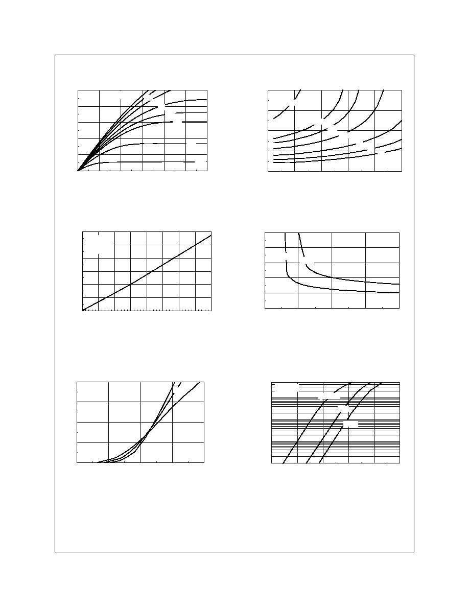
Typical Electrical Characteristics: N-Channel
0
0.1
0.2
0.3
0.4
0.5
0.6
0.8
1
1.2
1.4
I , DRAIN CURRENT (A)
DRAIN-SOURCE ON-RESISTANCE
V = 2.0V
GS
2.7
3.0
4.0
4.5
D
3.5
2.5
R
DS(on
)
, NORMALIZED
Figure 1. On-Region Characteristics.
Figure 2. On-Resistance Variation with
Drain Current and Gate Voltage.
Figure 3. On-Resistance Variation
with Temperature.
0.5
1
1.5
2
2.5
0
0.05
0.1
0.15
0.2
V , GATE TO SOURCE VOLTAGE (V)
I , DRAIN CURRENT (A)
25∞C
125∞C
V = 5.0V
DS
GS
D
T = -55∞C
J
Figure 5. Transfer Characteristics.
0.2
0.4
0.6
0.8
1
1.2
0.0001
0.001
0.01
0.1
0.2
0.5
V , BODY DIODE FORWARD VOLTAGE (V)
I , REVERSE DRAIN CURRENT (A)
T = 125∞C
J
25∞C
-55∞C
V = 0V
GS
SD
S
Figure 6. Body Diode Forward Voltage
Variation with Source Current and
Temperature.
Figure 4. On Resistance Variation with
Gate-To- Source Voltage.
2
2.5
3
3.5
4
0
3
6
9
12
15
V , GATE TO SOURCE VOLTAGE (V)
I = 0.2A
GS
R , ON-RESISTANCE (OHM)
DS(on)
125∞C
25∞C
D
-50
-25
0
25
50
75
100
125
150
0.6
0.8
1
1.2
1.4
1.6
1.8
T , JUNCTION TEMPERATURE (∞C)
DRAIN-SOURCE ON-RESISTANCE
J
V = 2.7 V
GS
I = 0.2A
D
R , NORMALIZED
DS(ON)
0
0.5
1
1.5
2
2.5
3
0
0.1
0.2
0.3
0.4
0.5
V , DRAIN-SOURCE VOLTAGE (V)
I , DRAIN-SOURCE CURRENT (A)
3.5
2.7
2.5
V = 4.5V
GS
4.0
2.0
1.5
DS
D
3.0
FDC6322C.Rev B1
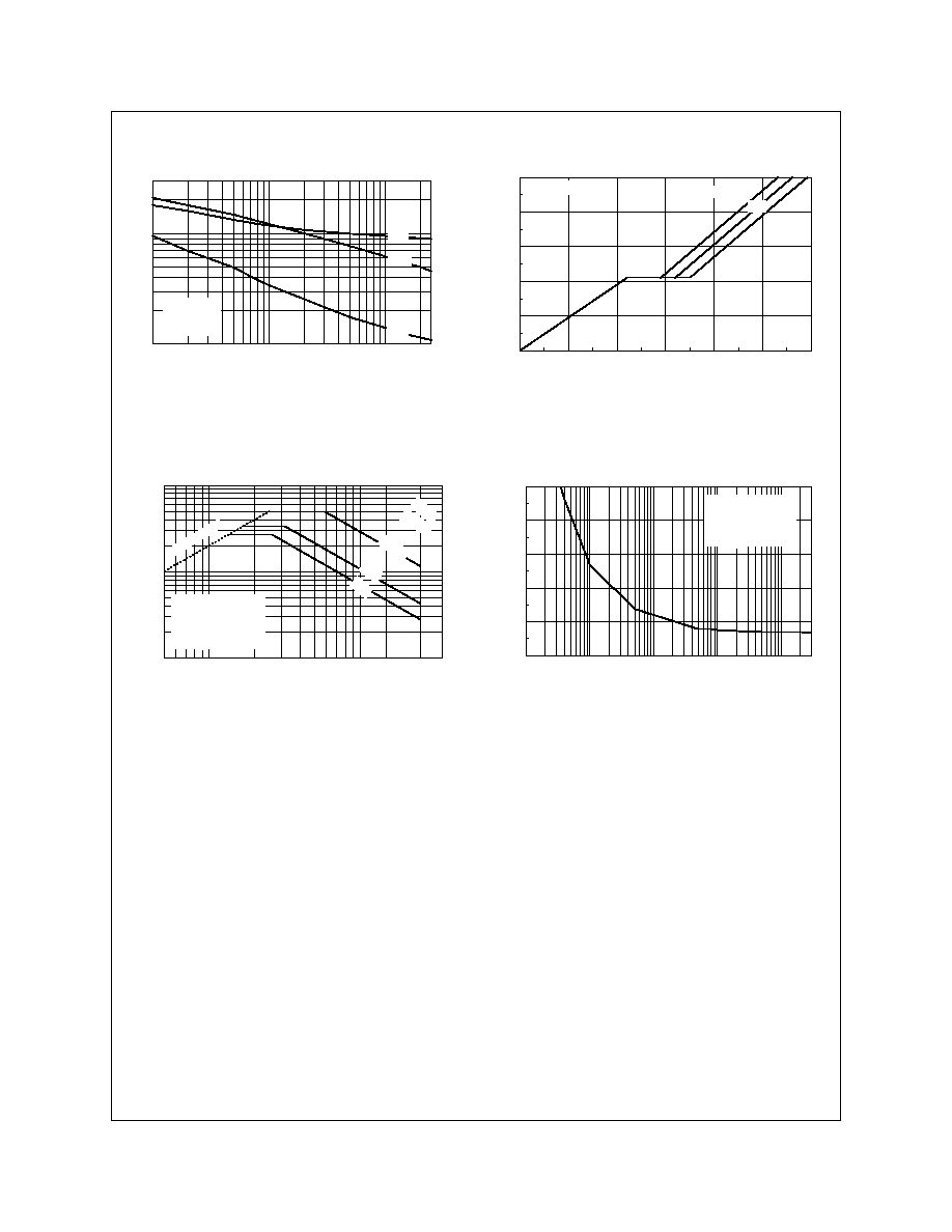
Figure 9. Maximum Safe Operating Area.
Figure 8. Gate Charge Characteristics
.
0.1
0.5
1
2
5
1 0
2 5
1
2
3
5
1 0
2 0
3 0
V , DRAIN TO SOURCE VOLTAGE (V)
CAPACITANCE (pF)
DS
C iss
f = 1 MHz
V = 0V
GS
C oss
C rss
Figure 7. Capacitance Characteristics.
Typical Electrical Characteristics: N-Channel
(continued)
0
0.1
0.2
0.3
0.4
0.5
0.6
0
1
2
3
4
5
Q , GATE CHARGE (nC)
V , GATE-SOURCE VOLTAGE (V)
g
GS
I = 0.2A
D
15V
V = 5V
DS
10V
0.5
1
2
5
10
15
25
35
0.01
0.02
0.05
0.1
0.2
0.5
1
V , DRAI N-SOURCE VOLTAGE (V)
I , DRAIN CURRENT (A)
DS
D
DC
1s
100ms
1ms
RDS(ON) LIMIT
V = 2.7V
SINGLE PULSE
R =See note 1b
T = 25∞C
GS
A
JA
10ms
0.01
0.1
1
10
100
300
0
1
2
3
4
5
SINGLE PULSE TIME (SEC)
POWER (W)
SINGLE PULSE
R =See note 1b
T = 25∞C
JA
A
Figure 10. Single Pulse Maximum Power
Dissipation.