 | ÐлекÑÑоннÑй компоненÑ: FDC6327C | СкаÑаÑÑ:  PDF PDF  ZIP ZIP |
Äîêóìåíòàöèÿ è îïèñàíèÿ www.docs.chipfind.ru
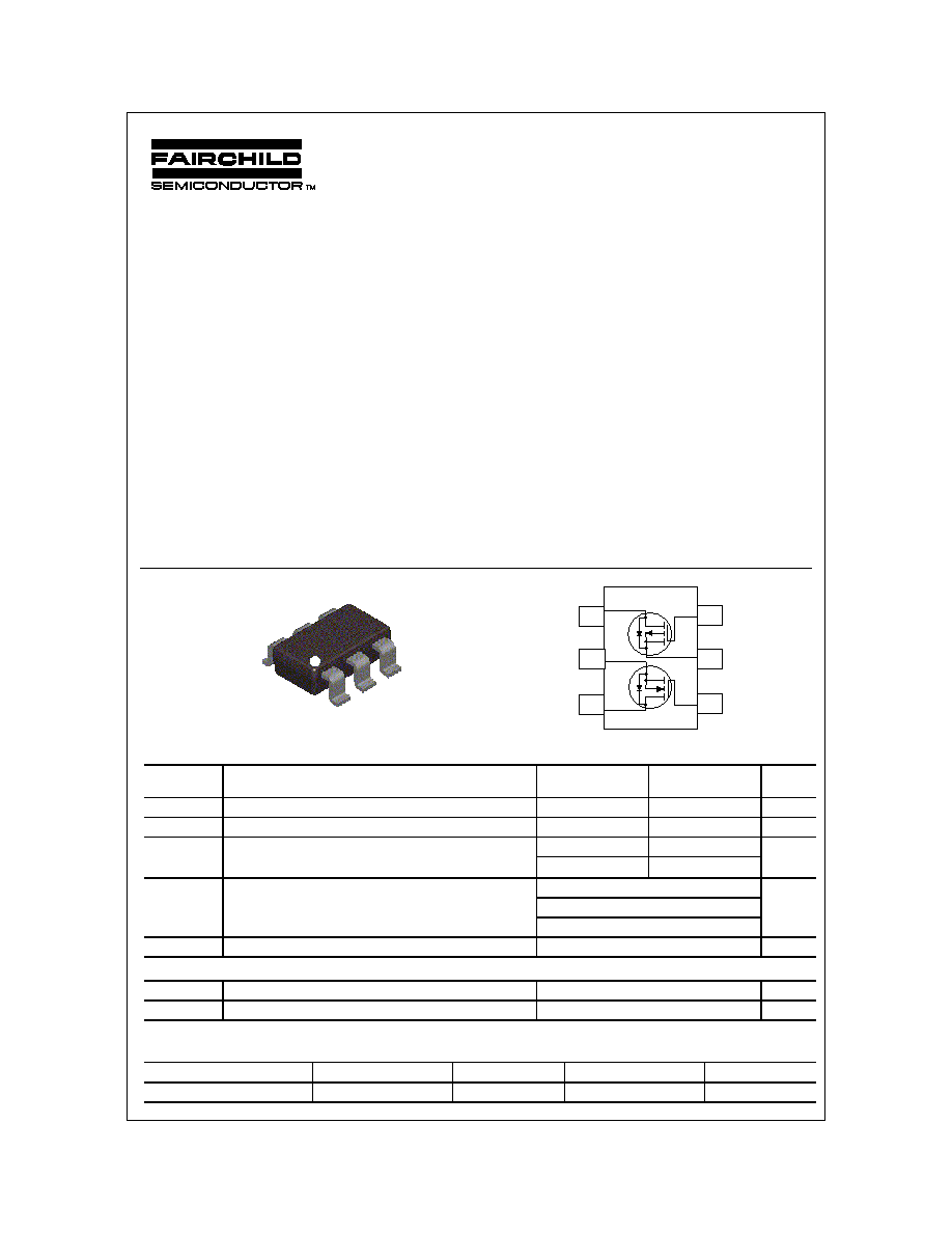
FDC6327C
FDC6327C, Rev. E
FDC6327C
Dual N & P-Channel 2.5V Specified PowerTrench
TM
MOSFET
General Description
These N & P-Channel 2.5V specified MOSFETs are
produced using Fairchild Semiconductor's advanced
PowerTrench process that has been especially tailored
to minimize on-state resistance and yet maintain low gate
charge for superior switching performance.
These devices have been designed to offer exceptional power
dissipation in a very small footprint for applications where
the bigger more expensive SO-8 and TSSOP-8 packages
are impractical.
Applications
·
DC/DC converter
·
Load switch
·
Motor driving
July 2000
Features
·
N-Channel 2.7A, 20V. R
DS(on)
= 0.08
@ V
GS
= 4.5V
R
DS(on)
= 0.12
@ V
GS
= 2.5V
·
P-Channel -1.6A, -20V.R
DS(on)
= 0.17
@ V
GS
= -4.5V
R
DS(on)
= 0.25
@ V
GS
= -2.5V
·
Fast switching speed.
·
Low gate charge.
·
High performance trench technology for extremely
low R
DS(ON)
.
·
SuperSOT
TM
-6 package: small footprint (72% smaller
than SO-8); low profile (1mm thick).
1999 Fairchild Semiconductor Corporation
Absolute Maximum Ratings
T
A
= 25°C unless otherwise noted
Symbol
Parameter
N-Channel
P-Channel
Units
V
DSS
Drain-Source Voltage
20
-20
V
V
GSS
Gate-Source Voltage
±
8
±
8
V
I
D
Drain Current - Continuous
(Note 1a)
2.7
-1.9
A
- Pulsed
8
-8
P
D
Power Dissipation
(Note 1a)
0.96
W
(Note 1b)
0.9
(Note 1c)
0.7
T
J
, T
stg
Operating and Storage Junction Temperature Range
-55 to +150
°
C
Thermal Characteristics
R
JA
Thermal Resistance, Junction-to-Ambient
(Note 1a)
130
°
C/W
R
JC
Thermal Resistance, Junction-to-Case
(Note 1)
60
°
C/W
Package Marking and Ordering Information
Device Marking
Device
Reel Size
Tape Width
Quantity
.327
FDC6327C
7"
8mm
3000
D1
S2
G1
D2
S1
G2
SuperSOT -6
TM
1
5
6
3
2
4
FDC6327C
FDC6327C, Rev. E
Electrical Characteristics
T
A
= 25°C unless otherwise noted
Symbol
Parameter
Test Conditions
Type Min Typ Max Units
Off Characteristics
BV
DSS
Drain-Source Breakdown
Voltage
V
GS
= 0 V, I
D
= 250
µ
A
V
GS
= 0 V, I
D
= - 250
µ
A
N-Ch
P-Ch
20
-20
V
BV
DSS
T
J
Breakdown Voltage
Temperature Coefficient
I
D
= 250
µ
A, Referenced to 25
°
C
I
D
= - 250
µ
A, Referenced to 25
°
C
N-Ch
P-Ch
12
-19
mV/
°
C
I
DSS
Zero Gate Voltage Drain
Current
V
DS
= 16 V, V
GS
= 0 V
V
DS
= -16 V, V
GS
= 0 V
N-Ch
P-Ch
1
-1
µ
A
I
GSSF
Gate-Body Leakage, Forward V
GS
= 8 V, V
DS
= 0 V
All
100
nA
I
GSSR
Gate-Body Leakage, Reverse V
GS
= -8 V, V
DS
= 0 V
All
-100
nA
On Characteristics
(Note 2)
V
GS(th)
Gate Threshold Voltage
V
DS
= V
GS
, I
D
= 250
µ
A
V
DS
= V
GS
, I
D
= -250
µ
A
N-Ch
P-Ch
0.4
-0.4
0.9
-0.9
1.5
-1.5
V
V
GS(th)
T
J
Gate Threshold Voltage
Temperature Coefficient
I
D
= 250
µ
A, Referenced to 25
°
C
I
D
= - 250
µ
A, Referenced to 25
°
C
N-Ch
P-Ch
-2.1
2.3
mV/
°
C
R
DS(on)
Static Drain-Source
On-Resistance
V
GS
= 4.5 V, I
D
= 2.7 A
V
GS
= 4.5 V, I
D
= 2.7 A, T
J
= 125
°
C
V
GS
= 2.5 V, I
D
= 2.2 A
V
GS
= -4.5 V, I
D
= -1.6 A
V
GS
= -4.5 V, I
D
= -1.6 A, T
J
= 125
°
C
V
GS
= -2.5 V, I
D
= -1.3 A
N-Ch
N-Ch
N-Ch
P-Ch
P-Ch
P-Ch
0.069
0.094
0.093
0.141
0.203
0.205
0.08
0.13
0.12
0.17
0.27
0.25
I
D(on)
On-State Drain Current
V
GS
= 4.5 V, V
DS
= 5 V
V
GS
= -4.5 V, V
DS
= -5 V
N-Ch
P-Ch
8
-8
A
g
FS
Forward Transconductance
V
DS
= 5 V, I
D
= 2.7 A
V
DS
= -5 V, I
D
= -1.9 A
N-Ch
P-Ch
7.7
4.5
S
Dynamic Characteristics
C
iss
Input Capacitance
N-Ch
P-Ch
325
315
pF
C
oss
Output Capacitance
N-Ch
P-Ch
75
65
pF
C
rss
Reverse Transfer Capacitance
N-Channel
V
DS
= 10 V, V
GS
= 0 V, f = 1.0 MHz
P-Channel
V
DS
= 10 V, V
GS
= 0 V, f = 1.0 MHz
N-Ch
P-Ch
35
24
pF
FDC6327C
FDC6327C, Rev. E
Electrical Characteristics
(continued)
T
A
= 25°C unless otherwise noted
Symbol
Parameter
Test Conditions
Type Min
Typ Max Units
Switching Characteristics
(Note 2)
t
d(on)
Turn-On Delay Time
N-Ch
P-Ch
5
7
15
14
ns
t
r
Turn-On Rise Time
N-Ch
P-Ch
9
14
18
25
ns
t
d(off)
Turn-Off Delay Time
N-Ch
P-Ch
12
14
22
25
ns
t
f
Turn-Off Fall Time
N-Channel
V
DD
= 10 V, I
D
= 1 A,
V
GS
= 4.5V, R
GEN
= 6
P-Channel
V
DD
= -10 V, I
D
= -1 A,
V
GS
= -4.5 V, R
GEN
= 6
N-Ch
P-Ch
3
3
9
9
ns
Q
g
Total Gate Charge
N-Ch
P-Ch
3.25
2.85
4.5
4.0
nC
Q
gs
Gate-Source Charge
N-Ch
P-Ch
0.65
0.68
nC
Q
gd
Gate-Drain Charge
N-Channel
V
DS
= 10 V, I
D
= 2.7 A, V
GS
= 4.5V
P-Channel
V
DS
= -10 V, I
D
= -1.9 A,V
GS
= -4.5V
N-Ch
P-Ch
0.90
0.65
nC
Drain-Source Diode Characteristics and Maximum Ratings
I
S
Maximum Continuous Drain-Source Diode Forward Current
N-Ch
P-Ch
0.8
-0.8
A
V
SD
Drain-Source Diode Forward
Voltage
V
GS
= 0 V, I
S
= 0.8 A
(Note 2)
V
GS
= 0 V, I
S
= - 0.8 A
(Note 2)
N-Ch
P-Ch
0.76
-0.79
1.2
-1.2
V
Notes:
1: R
JA
is the sum of the junction-to-case and case-to-ambient resistance where the case thermal reference is defined as the solder mounting surface of the drain pins.
R
JC
is guaranteed by design while R
JA
is determined by the user's board design. Both devices are assumed to be operating and sharing the dissipated heat energy
equally.
Scale 1 : 1 on letter size paper
2: Pulse Test: Pulse Width
300
µ
s, Duty Cycle
2.0%
a) 130
°
C/W when
mounted on a 0.125 in
2
pad of 2 oz. copper.
b) 140
°
C/W when
mounted on a 0.005 in
2
pad of 2 oz. copper.
c) 180
°
C/W when
mounted on a 0.0015 in
2
pad of 2 oz. copper.
FDC6327C
FDC6327C, Rev. E
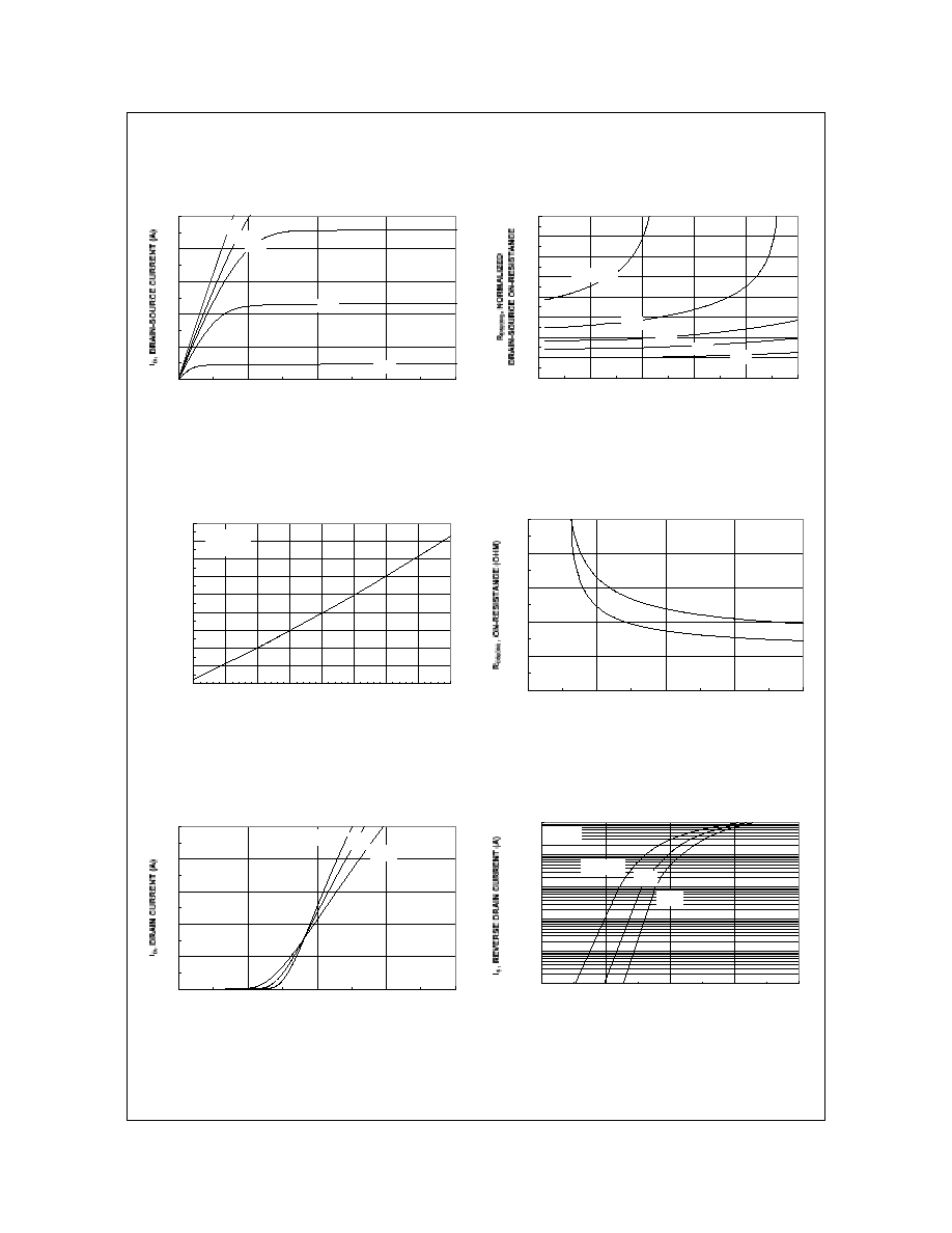
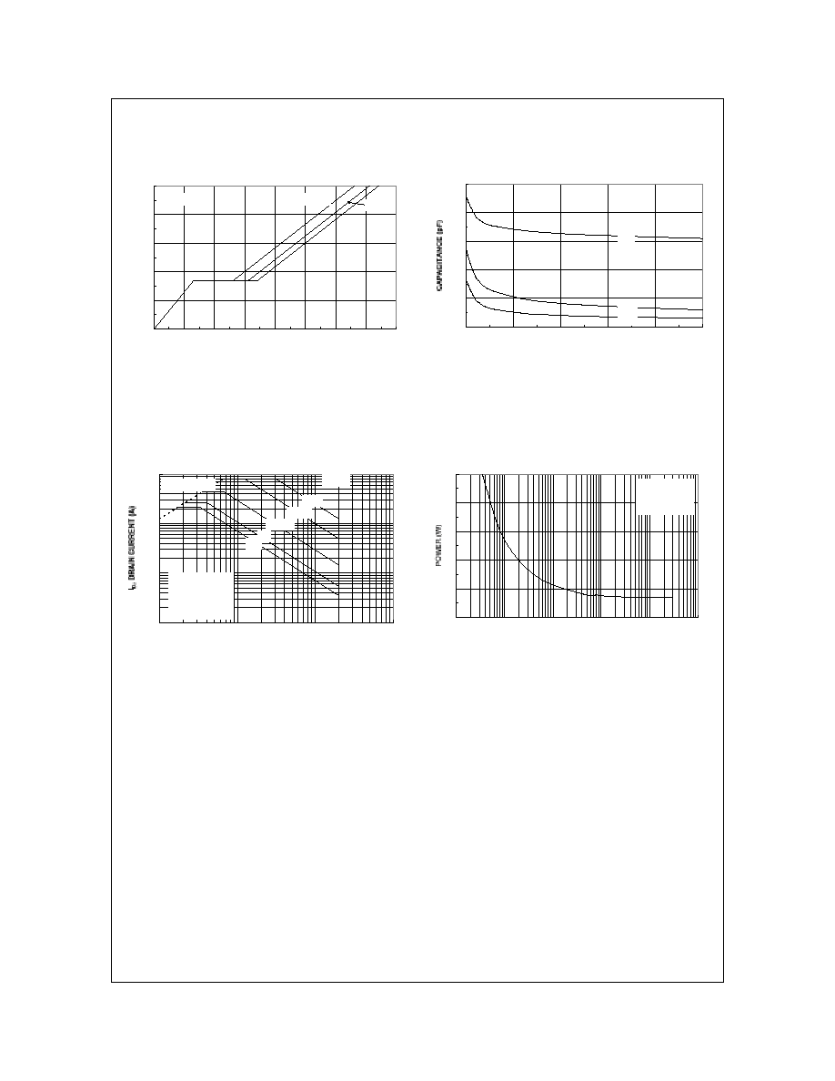
Typical Characteristics: N-Channel
Figure 5. Transfer Characteristics.
Figure 6. Body Diode Forward Voltage
Variation with Source Current
and Temperature.
0
2
4
6
8
10
0
1
2
3
4
V
DS
, DRAIN-SOURCE VOLTAGE (V)
V
GS
= 4.5V
3.0V
2.5V
2.0V
1.5V
0.8
1
1.2
1.4
1.6
1.8
2
2.2
2.4
0
2
4
6
8
10
I
D
, DRAIN CURRENT (A)
V
GS
= 2.0V
2.5V
3.0V
3.5V
4.5V
0
2
4
6
8
10
0
1
2
3
4
V
GS
, GATE TO SOURCE VOLTAGE (V)
T
A
= -55
o
C
25
o
C
125
o
C
V
DS
= 5V
0.0001
0.001
0.01
0.1
1
10
0
0.4
0.8
1.2
1.6
V
SD
, BODY DIODE FORWARD VOLTAGE (V)
T
A
= 125
o
C
25
o
C
-55
o
C
V
GS
= 0V
Figure 3. On-Resistance Variation
with Temperature.
Figure 4. On-Resistance Variation
with Gate-to-Source Voltage.
0
0.05
0.1
0.15
0.2
0.25
1
2
3
4
5
V
GS
, GATE TO SOURCE VOLTAGE (V)
I
D
= 1.3A
T
A
= 125
o
C
T
A
= 25
o
C
0.7
0.8
0.9
1
1.1
1.2
1.3
1.4
1.5
1.6
-50
-25
0
25
50
75
100
125
150
T
J
, JUNCTION TEMPERATURE (
o
C)
R
DS
(O
N)
,
NO
RMALI
Z
E
D
DRAI
N-S
O
UR
CE
O
N
-RE
S
I
S
T
ANCE
I
D
= 2.7A
V
GS
= 4.5V
Figure 1. On-Region Characteristics.
Figure 2. On-Resistance Variation
with Drain Current and Gate Voltage.
FDC6327C
FDC6327C, Rev. E
Typical Characteristics: N-Channel
(continued)
0
100
200
300
400
500
0
4
8
12
16
20
V
DS
, DRAIN TO SOURCE VOLTAGE (V)
C
ISS
C
RSS
C
OSS
f = 1MHz
V
GS
= 0 V
0.01
0.1
1
10
0.1
1
10
100
V
DS
, DRAIN-SOURCE VOLTAGE (V)
DC
1s
100ms
10ms
1ms
100
µ
s
R
DS(ON)
LIMIT
V
GS
= 4.5V
SINGLE PULSE
R
JA
= 180
o
C/W
T
A
= 25
o
C
0
1
2
3
4
5
0.01
0.1
1
10
100
1000
SINGLE PULSE TIME (SEC)
SINGLE PULSE
R
JA
= 180
o
C/W
T
A
= 25
o
C
Figure 7. Gate-Charge Characteristics.
Figure 8. Capacitance Characteristics.
0
1
2
3
4
5
0
0.5
1
1.5
2
2.5
3
3.5
4
Q
g
, GATE CHARGE (nC)
V
GS
,
G
A
TE
-
S
O
URCE
V
O
LTAG
E
(V
)
I
D
= 2.7A
V
DS
= 5V
10V
15V
Figure 9. Maximum Safe Operating Area.
Figure 10. Single Pulse Maximum
Power Dissipation.