 | –≠–ª–µ–∫—Ç—Ä–æ–Ω–Ω—ã–π –∫–æ–º–ø–æ–Ω–µ–Ω—Ç: FDC654P | –°–∫–∞—á–∞—Ç—å:  PDF PDF  ZIP ZIP |
March 1998
FDC654P
P-Channel Enhancement Mode Field Effect Transistor
General Description
Features
Absolute Maximum Ratings
T
A
= 25∞C unless otherwise note
Symbol Parameter
FDC654P
Units
V
DSS
Drain-Source Voltage
-30
V
V
GSS
Gate-Source Voltage - Continuous
±20
V
I
D
Drain Current - Continuous
(Note 1a)
-3.6
A
- Pulsed
-10
P
D
Maximum Power Dissipation
(Note 1a)
1.6
W
(Note 1b)
0.8
T
J
,T
STG
Operating and Storage Temperature Range
-55 to 150
∞C
THERMAL CHARACTERISTICS
R
JA
Thermal Resistance, Junction-to-Ambient
(Note 1a)
78
∞C/W
R
JC
Thermal Resistance, Junction-to-Case
(Note 1)
30
∞C/W
FDC654P Rev.C
These P-Channel logic level enhancement mode power field
effect transistors are produced using Fairchild's proprietary,
high cell density, DMOS technology. This very high density
process is especially tailored to minimize on-state
resistance. These devices are particularly suited for low
voltage applications such as cellular phone and notebook
computer power management and other battery powered
circuits where high-side switching, and low in-line power
loss are needed in a very small outline surface mount
package.
-3.6 A, -30 V. R
DS(ON)
= 0.075
@ V
GS
= -10 V
R
DS(ON)
= 0.125
@ V
GS
= -4.5 V.
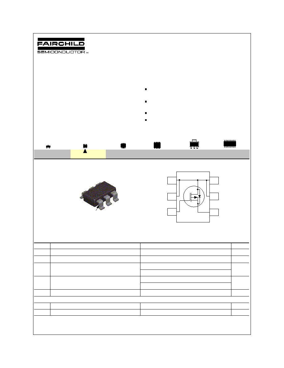
SuperSOT
TM
-6 package design using copper lead frame for
superior thermal and electrical capabilities.
High density cell design for extremely low R
DS(ON)
.
Exceptional on-resistance and maximum DC current capability.
SOIC-16
SOT-23
SuperSOT
TM
-8
SO-8
SOT-223
SuperSOT
TM
-6
D
D
D
S
D
G
SuperSOT -6
TM
.654
pin
1
3
5
6
4
1
2
3
© 1998 Fairchild Semiconductor Corporation

ELECTRICAL CHARACTERISTICS
(T
A
= 25∞C unless otherwise noted)
Symbol
Parameter
Conditions
Min
Typ
Max
Units
OFF CHARACTERISTICS
BV
DSS
Drain-Source Breakdown Voltage
V
GS
= 0 V, I
D
= -250 µA
-30
V
BV
DSS
/
T
J
Breakdown Voltage Temp. Coefficient
I
D
= -250 µA, Referenced to 25
o
C
-29
mV /
o
C
I
DSS
Zero Gate Voltage Drain Current
V
DS
= -24 V, V
GS
= 0 V
-1
µA
T
J
= 55
o
C
-10
µA
I
GSSF
Gate - Body Leakage, Forward
V
GS
= 20 V, V
DS
= 0 V
100
nA
I
GSSR
Gate - Body Leakage, Reverse
V
GS
= -20 V, V
DS
= 0 V
-100
nA
ON CHARACTERISTICS
(Note 2)
V
GS(th)
Gate Threshold Voltage
V
DS
= V
GS
, I
D
= -250 µA
-1
-1.7
-3
V
V
GS(th)
/
T
J
Gate Threshold VoltageTemp.Coefficient
I
D
= -250 µA, Referenced to 25
o
C
3.6
mV /
o
C
R
DS(ON)
Static Drain-Source On-Resistance
V
GS
= -10 V, I
D
= -3.6 A
0.065
0.075
T
J
= 125
o
C
0.094
0.127
V
GS
= -4.5 V, I
D
= -2.7 A
0.11
0.125
I
D(on)
On-State Drain Current
V
GS
= -4.5 V, V
DS
= -5 V
-5
A
g
FS
Forward Transconductance
V
DS
= -10 V, I
D
= -3.6 A
3
S
DYNAMIC CHARACTERISTICS
C
iss
Input Capacitance
V
DS
= -15 V, V
GS
= 0 V,
435
pF
C
oss
Output Capacitance
f = 1.0 MHz
245
pF
C
rss
Reverse Transfer Capacitance
70
pF
SWITCHING CHARACTERISTICS
(Note 2)
t
D(on)
Turn - On Delay Time
V
DD
= -15 V, I
D
= -1 A,
10
18
ns
t
r
Turn - On Rise Time
V
GS
= -10 V, R
GEN
= 6
7
14
ns
t
D(off)
Turn - Off Delay Time
26
42
ns
t
f
Turn - Off Fall Time
18
29
ns
Q
g
Total Gate Charge
V
DS
= -15 V, I
D
= -3.6 A,
10.5
15
nC
Q
gs
Gate-Source Charge
V
GS
= -10 V
2
nC
Q
gd
Gate-Drain Charge
2.6
nC
DRAIN-SOURCE DIODE CHARACTERISTICS
I
S
Continuous Source Diode Current
-1.3
A
V
SD
Drain-Source Diode Forward Voltage
V
GS
= 0 V, I
S
= -1.3 A
(Note 2)
-0.8
-1.2
V
T
J
= 125
o
C
-0.62
-1
Notes:
1. R
JA
is the sum of the junction-to-case and case-to-ambient thermal resistance where the case thermal reference is defined as the solder mounting surface of the drain pins. R
JC
is guaranteed by
design while R
CA
is determined by the user's board design.
a. 78
o
C/W when mounted on a minimum on a 1 in
2
pad of 2oz Cu in FR-4 board.
b. 156
o
C/W when mounted on a minimum pad of 2oz Cu in FR-4 board.
2. Pulse Test: Pulse Width < 300µs, Duty Cycle < 2.0%.
FDC654P Rev.C
FDC654P Rev.C
0
1
2
3
4
5
0
3
6
9
12
15
-V , DRAIN-SOURCE VOLTAGE (V)
-I , DRAIN-SOURCE CURRENT (A)
V = -10V
GS
DS
D
-6.0
-5.0
-3.0
-4.0
-3.5
-4.5
0
3
6
9
12
15
0.5
1
1.5
2
-I , DRAIN CURRENT (A)
DRAIN-SOURCE ON-RESISTANCE
V = -3.5 V
GS
D
R , NORMALIZED
DS(ON)
-10
-4.5
-4.0
-6.0
-5.0
-5.5
-7.0
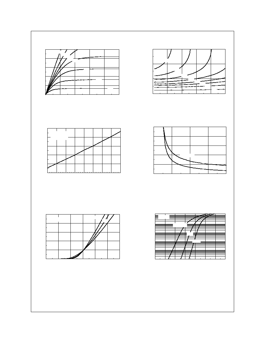
Typical Electrical Characteristics
Figure 1. On-Region Characteristics.
Figure 2. On-Resistance Variation with
Drain Current and Gate Voltage.
Figure 3. On-Resistance Variation
with Temperature.
Figure 5. Transfer Characteristics.
0
0.2
0.4
0.6
0.8
1
1.2
1.4
0.0001
0.001
0.01
0.1
1
15
-V , BODY DIODE FORWARD VOLTAGE (V)
-I , REVERSE DRAIN CURRENT (A)
T = 125∞C
J
25∞C
-55∞C
V = 0V
GS
SD
S
Figure 4. On-Resistance Variation with
Gate-to-Source Voltage.
2
4
6
8
10
0.05
0.1
0.15
0.2
0.25
0.3
-V , GATE TO SOURCE VOLTAGE (V)
GS
R , ON-RESISTANCE (OHM)
DS(ON)
I = -1.8A
D
T = 125∞C
A
25∞C
0
0.5
1
1.5
2
2.5
3
0
3
6
9
12
15
-V , GATE TO SOURCE VOLTAGE (V)
-I , DRAIN CURRENT (A)
V = -5.0V
DS
GS
D
T = -55∞C
J
125∞C
25∞C
Figure 6. Body Diode Forward Voltage
Variation with Source Current
and Temperature.
-50
-25
0
25
50
75
100
125
150
0.6
0.8
1
1.2
1.4
1.6
T , JUNCTION TEMPERATURE (∞C)
DRAIN-SOURCE ON-RESISTANCE
J
R , NORMALIZED
DS(ON)
V = -10V
GS
I = -3.6A
D
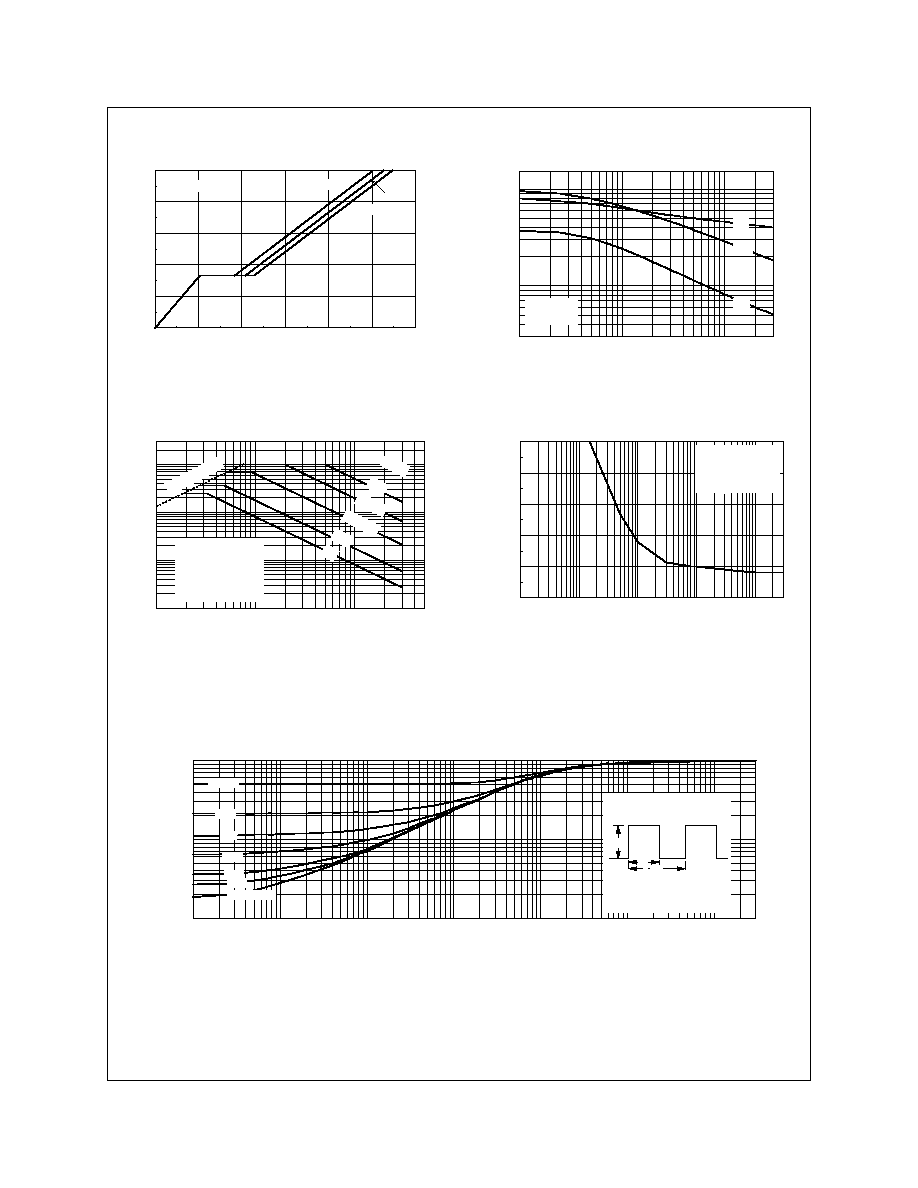
FDC654P Rev.C
Figure 10. Single Pulse Maximum Power
Dissipation.
0.1
0.2
0.5
1
2
5
10
30
30
80
200
600
1500
-V , DRAIN TO SOURCE VOLTAGE (V)
CAPACITANCE (pF)
DS
C
iss
f = 1 MHz
V = 0 V
GS
C
oss
C
rss
Figure 8. Capacitance Characteristics.
Figure 7. Gate Charge Characteristics.
Figure 9. Maximum Safe Operating Area.
Typical Electrical And Thermal Characteristics
0
2
4
6
8
10
12
0
2
4
6
8
10
Q , GATE CHARGE (nC)
-V , GATE-SOURCE VOLTAGE (V)
g
GS
V = -5V
DS
-10V
-15V
I = -3.6A
D
0.1
0.2
0.5
1
2
5
10
30
50
0.01
0.03
0.1
0.3
1
3
10
30
- V , DRAIN-SOURCE VOLTAGE (V)
-I , DRAIN CURRENT (A)
RDS(ON) LIMIT
D
A
DC
DS
1s
100ms
10ms
1ms
V = -10V
SINGLE PULSE
R = See Note 1b
T = 25∞C
JA
GS
A
100us
0.0001
0.001
0.01
0.1
1
10
100
300
0.01
0.02
0.05
0.1
0.2
0.5
1
t , TIME (sec)
TRANSIENT THERMAL RESISTANCE
1
Single Pulse
D = 0.5
0.1
0.05
0.02
0.01
0.2
r(t), NORMALIZED EFFECTIVE
Duty Cycle, D = t / t
1
2
R (t) = r(t) * R
R = See Note 1b
JA
JA
JA
T - T = P * R (t)
JA
A
J
P(pk)
t
1
t
2
Figure 11. Transient Thermal Response Curve.
Note: Thermal characterization performed using the conditions described in note 1b.
Transient thermal response will change depending on the circuit board design.
0.01
0.1
1
10
100
300
0
1
2
3
4
5
SINGLE PULSE TIME (SEC)
POWER (W)
SINGLE PULSE
R =See note 1b
T = 25∞C
JA
A