 | ÐлекÑÑоннÑй компоненÑ: FDC655BN | СкаÑаÑÑ:  PDF PDF  ZIP ZIP |
Äîêóìåíòàöèÿ è îïèñàíèÿ www.docs.chipfind.ru
©2005 Fairchild Semiconductor Corporation
1
www.fairchildsemi.com
April 2005
FDC655BN Rev. C(W)
FDC655BN Single N-Channel,
Logic Le
vel,
P
o
werT
renc
h
®
MOSFET
FDC655BN
Single N-Channel, Logic Level, PowerTrench
®
MOSFET
Features
6.3 A, 30 V.
R
DS(ON)
= 25 m
@ V
GS
= 10 V
R
DS(ON)
= 33 m
@ V
GS
= 4.5 V
Fast switching
Low gate charge
High performance trench technology for extremely low Rdson
General Description
This N-Channel Logic Level MOSFET is produced using Fair-
child Semiconductor's advanced PowerTrench process that has
been especially tailored to minimized on-state resistance and
yet maintain superior switching performance.
These devices are well suited for low voltage and battery pow-
ered applications where low in-line power loss and fast switch-
ing are required.
Absolute Maximum Ratings
T
A
= 25°C unless otherwise noted
Package Marking and Ordering Information
Symbol
Parameter
Ratings
Units
V
DSS
Drain-Source Voltage
30
V
V
GSS
Gate-Source Voltage
±
20
V
I
D
Drain Current
Continuous
(Note 1a)
6.3
A
Pulsed
20
P
D
Maximum Power Dissipation
(Note 1a)
1.6
W
(Note 1b)
0.8
T
J
, T
STG
Operating and Storage Junction Temperature Range
55 to +150
°
C
Thermal Characteristics
R
JA
Thermal Resistance, Junction-to-Ambient
(Note 1a)
78
°
C/W
R
JC
Thermal Resistance, Junction-to-Case
(Note 1)
30
°
C/W
Device Marking
Device
Reel Size
Tape width
Quantity
.55B
FDC655BN
7''
8mm
3000 units
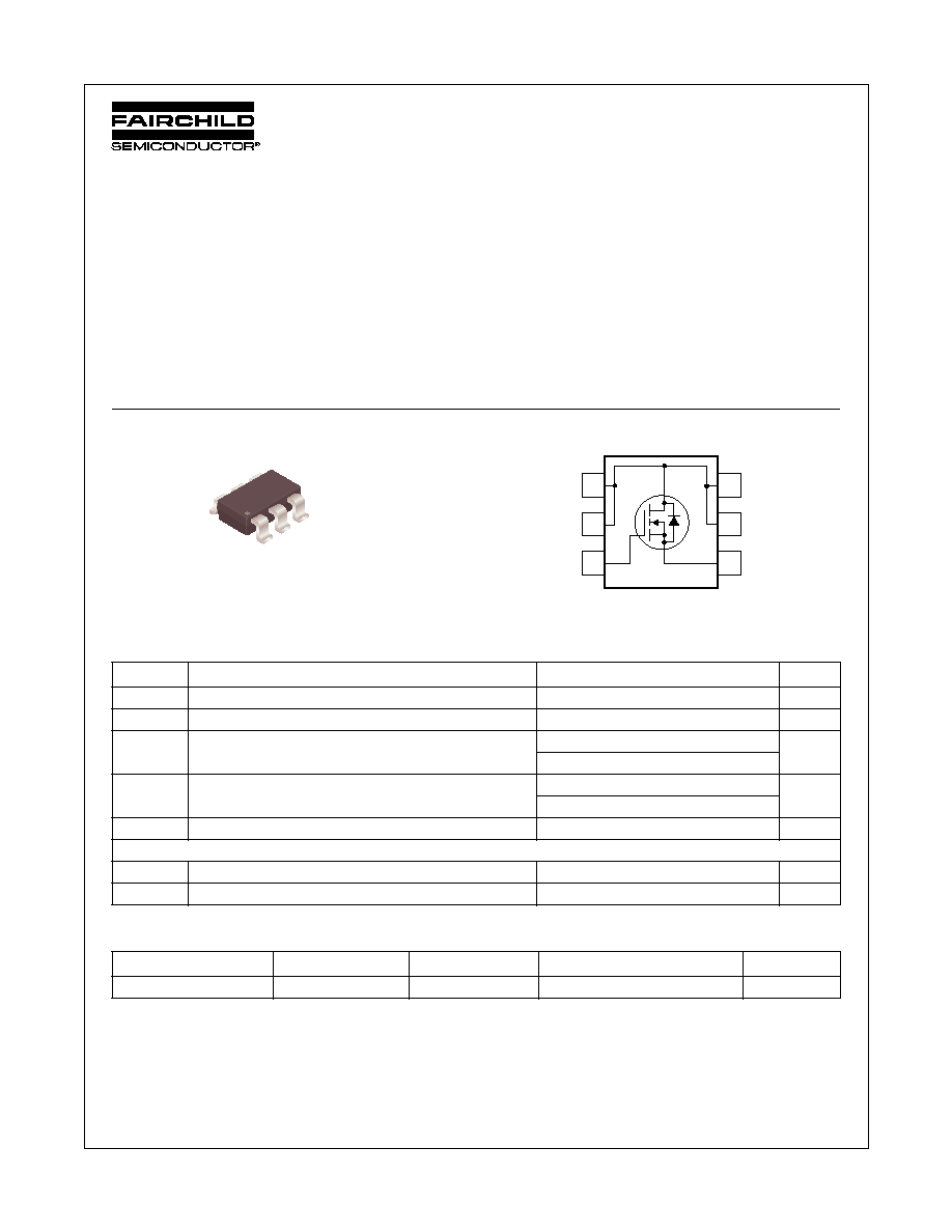
1
2
3
6
5
4
D
D
SuperSOT-6
TM
D
G
D
55B
S
2
www.fairchildsemi.com
FDC655BN Rev. C(W)
FDC655BN Single N-Channel,
Logic Le
vel,
P
o
werT
renc
h
®
MOSFET
Electrical Characteristics
T
A
= 25°C unless otherwise noted
Notes:
1.
R
JA
is the sum of the junction-to-case and case-to-ambient resistance where the case thermal reference is defined as the solder mounting surface of the drain pins. R
JC
is
guaranteed by design while R
CA
is determined by the user's board design.
a.
78°C/W when mounted on a 1in
2
pad of 2oz copper on FR-4 board.
b.
156°C/W when mounted on a minimum pad.
2.
Pulse Test: Pulse Width
300
µ
s, Duty Cycle
2.0%
Symbol
Parameter
Test Conditions
Min
Typ
Max
Units
Off Characteristics
BV
DSS
DrainSource Breakdown Voltage
V
GS
= 0 V, I
D
= 250
µ
A
30
V
BV
DSS
T
J
Breakdown Voltage Temperature
Coefficient
I
D
= 250
µ
A, Referenced to 25
°
C
23
mV/
°
C
I
DSS
Zero Gate Voltage Drain Current
V
DS
= 24 V, V
GS
= 0 V
V
DS
= 24 V, V
GS
= 0 V, T
J
= -55
°
C
1
10
µ
A
I
GSS
GateBody Leakage
V
GS
=
±
20 V, V
DS
= 0 V
±
100
nA
On Characteristics
(Note 2)
V
GS(th)
Gate Threshold Voltage
V
DS
= V
GS
, I
D
= 250
µ
A
1
1.9
3
V
V
GS(th)
T
J
Gate Threshold Voltage
Temperature Coefficient
I
D
= 250
µ
A, Referenced to 25
°
C
4.1
mV/
°
C
R
DS(on)
Static DrainSource
OnResistance
V
GS
= 10 V, I
D
= 6.3 A
V
GS
= 4.5 V, I
D
= 5.5 A
V
GS
= 10 V, I
D
= 6.3 A, T
J
=125
°
C
20
26
27
25
33
45
m
g
FS
Forward Transconductance
V
DS
= 10 V, I
D
= 6.3 A
20
S
Dynamic Characteristics
C
iss
Input Capacitance
V
DS
= 15 V, V
GS
= 0 V,
f = 1.0 MHz
570
pF
C
oss
Output Capacitance
140
pF
C
rss
Reverse Transfer Capacitance
70
pF
R
G
Gate Resistance
V
GS
= 15 mV, f = 1.0 MHz
2.1
Switching Characteristics
(Note 2)
t
d(on)
TurnOn Delay Time
V
DD
= 15 V, I
D
= 1 A,
V
GS
= 10 V, R
GEN
= 6
8
16
ns
t
r
TurnOn Rise Time
4
8
ns
t
d(off)
TurnOff Delay Time
22
35
ns
t
f
TurnOff Fall Time
3
6
ns
Q
g(TOT)
Total Gate Charge at Vgs=10V
V
DD
= 15 V, I
D
= 6.3 A,
10
15
nC
Q
g(TOT)
Total Gate Charge at Vgs=5V
6
8
nC
Q
gs
GateSource Charge
1.7
nC
Q
gd
GateDrain Charge
2.1
nC
DrainSource Diode Characteristics and Maximum Ratings
I
S
Maximum Continuous DrainSource Diode Forward Current
1.3
A
V
SD
DrainSource Diode Forward Voltage V
GS
= 0 V, I
S
= 1.3 A (Note 2)
0.8
1.2
V
t
rr
Diode Reverse Recovery Time
I
F
= 6.3 A, d
IF
/d
t
= 100 A/
µ
s
18
ns
Q
rr
Diode Reverse Recovery Charge
9
nC
3
www.fairchildsemi.com
FDC655BN Rev. C(W)
FDC655BN Single N-Channel,
Logic Le
vel,
P
o
werT
renc
h
®
MOSFET
Typical Characteristics
0
5
10
15
20
25
0
1
2
3
V
DS
, DRAIN-SOURCE VOLTAGE (V)
I
D
, DRAIN CURRENT (A)
6.0V
3.5V
4.5V
3.0V
V
GS
= 10V
4.0V
0.8
1
1.2
1.4
1.6
1.8
2
2.2
0
5
10
15
20
25
I
D
, DRAIN CURRENT (A)
R
DS(ON)
, NORMALIZED
DRAIN-SOURCE ON-RESISTANCE
V
GS
= 3.5V
6.0V
4.0V
4.5V
5.0V
10V
Figure 1. On-Region Characteristics.
Figure 2. On-Resistance Variation with
Drain Current and Gate Voltage.
0.6
0.8
1
1.2
1.4
1.6
-50
-25
0
25
50
75
100
125
150
T
J
, JUNCTION TEMPERATURE (
°C)
R
DS(ON)
, NORMALIZED
DRAIN-SOURCE ON-RESISTANCE
I
D
= 6.3A
V
GS
= 10.0V
0.01
0.03
0.05
0.07
0.09
2
4
6
8
10
V
GS
, GATE TO SOURCE VOLTAGE (V)
R
DS(ON)
, ON-RESISTANCE (OHM)
I
D
= 3.2A
T
A
= 125
o
C
T
A
= 25
o
C
Figure 3. On-Resistance Variation
withTemperature.
Figure 4. On-Resistance Variation with
Gate-to-Source Voltage.
0
5
10
15
20
25
1.5
2
2.5
3
3.5
4
4.5
V
GS
, GATE TO SOURCE VOLTAGE (V)
I
D
, DRAIN CURRENT (A)
T
A
= 125
°C
-55
°C
V
DS
= 5V
25
°C
0.0001
0.001
0.01
0.1
1
10
100
0
0.2
0.4
0.6
0.8
1
1.2
1.4
V
SD
, BODY DIODE FORWARD VOLTAGE (V)
I
S
, REVERSE DRAIN CURRENT (A)
T
A
= 125
°C
25
°C
-55
°C
V
GS
= 0V
Figure 5. Transfer Characteristics.
Figure 6. Body Diode Forward Voltage Variation
with Source Current and Temperature.
4
www.fairchildsemi.com
FDC655BN Rev. C(W)
FDC655BN Single N-Channel,
Logic Le
vel,
P
o
werT
renc
h
®
MOSFET
Typical Characteristics
0
2
4
6
8
10
0
2
4
6
8
10
12
Q
g
, GATE CHARGE (nC)
V
GS
, GATE-SOURCE VOLTAGE (V)
I
D
= 6.3A
15V
20V
0
200
400
600
800
0
5
10
15
20
25
30
V
DS
, DRAIN TO SOURCE VOLTAGE (V)
CAPACITANCE (pF)
C
iss
C
rss
C
oss
f = 1MHz
V
GS
= 0 V
Figure 7. Gate Charge Characteristics.
Figure 8. Capacitance Characteristics.
0.01
0.1
1
10
100
0.1
1
10
100
V
DS
, DRAIN-SOURCE VOLTAGE (V)
I
D
, DRAIN CURRENT (A)
DC
10s
1s
100ms
100
µs
R
DS(ON)
LIMIT
V
GS
= 10.0V
SINGLE PULSE
R
JA
= 156
o
C/W
T
A
= 25
o
C
10ms
1ms
0
1
2
3
4
5
0.1
1
10
100
1000
t
1
, TIME (sec)
P(pk), PEAK TRANSIENT POWER (W)
SINGLE PULSE
R
JA
= 156
°C/W
T
A
= 25
°C
Figure 9. Maximum Safe Operating Area.
Figure 10. Single Pulse Maximum
Power Dissipation.
0.001
0.01
0.1
1
0.0001
0.001
0.01
0.1
1
10
100
1000
t
1
, TIME (sec)
r(t), NORMALIZED EFFECTIVE
TRANSIENT THERMAL RESISTANCE
R
JA
(t) = r(t) * R
JA
R
JA
= 156
°C/W
T
J
- T
A
= P * R
JA
(t)
Duty Cycle, D = t
1
/ t
2
t
1
SINGLE PULSE
0.01
0.02
0.05
0.1
0.2
D = 0.5
Figure 11. Transient Thermal Response Curve.
Thermal characterization performed using the conditions described in Note 1c.
Transient thermal response will change depending on the circuit board design.
V
DS
= 10V
t
2
P(pk)
5
www.fairchildsemi.com
FDC655BN Rev. C(W)
FDC655BN Single N-Channel,
Logic Le
vel,
P
o
werT
renc
h
®
MOSFET
Typical Characteristics
V
DS
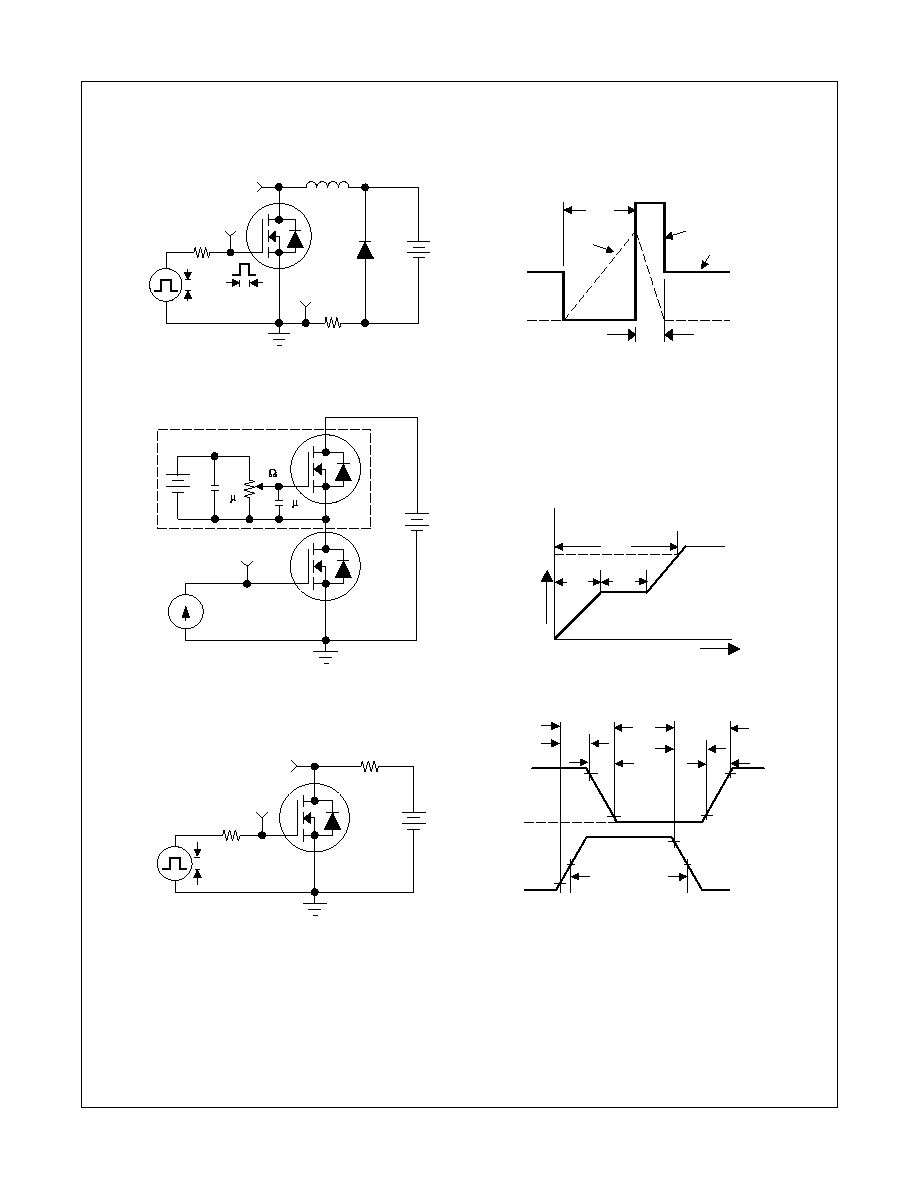
L
Figure 12. Unclamped Inductive
Load Test Circuit
Figure 14. Gate Charge Test Circuit
Figure 15. Gate Charge Waveform
Figure 16. Switching Time
Test Circuit
Figure 17. Switching Time Waveforms
Figure 13. Unclamped Inductive
Waveforms
R
GE
DUT
V
GS
I
AS
0.01
V
DD
+
tp
0V
vary t
P
to obtain
required peak I
AS
V
GS
t
AV
t
P
I
AS
V
DS
V
DD
BV
DSS
V
DS
R
L
R
GEN
DUT
V
DD
V
GS
Pulse Width
1µs
Duty Cycle
0.1%
V
GS
+
t
r
t
f
t
d(ON)
t
d(OFF)
t
ON
t
OFF
Pulse Width
10%
10%
90%
10%
90%
50%
90%
50%
0V
0V
V
GS
V
DS
V
GS
Q
GS
Q
GD
Q
G(TOT)
10V
Charge, (nC)
DUT
V
DD
V
GS
I
g(REF)
+
+
-
Same type as DUT
Drain Current
1 F
10 F
10V
50k