 | ÐлекÑÑоннÑй компоненÑ: FDD3570 | СкаÑаÑÑ:  PDF PDF  ZIP ZIP |
Äîêóìåíòàöèÿ è îïèñàíèÿ www.docs.chipfind.ru
February 2000
PRELIMINARY
2000 Fairchild Semiconductor Corporation
FDD3570 Rev BW)
FDD3570
80V N-Channel PowerTrench
MOSFET
General Description
This N-Channel Logic level MOSFET has been
designed specifically to improve the overall efficiency of
DC/DC converters using either synchronous or
conventional switching PWM controllers.
This MOSFET features faster switching and lower gate
change than other MOSFETs with comparable R
DS(ON)
specifications resulting in DC/DC power supply designs
with higher overall efficiency.
Features
·
10 A, 80 V.
R
DS(ON)
= 0.019
@ V
GS
= 10 V
R
DS(ON)
= 0.022
@ V
GS
= 6 V.
·
Fast switching speed.
·
High performance trench technology for extremely
low R
DS(ON)
.
·
High power and current handling capability.
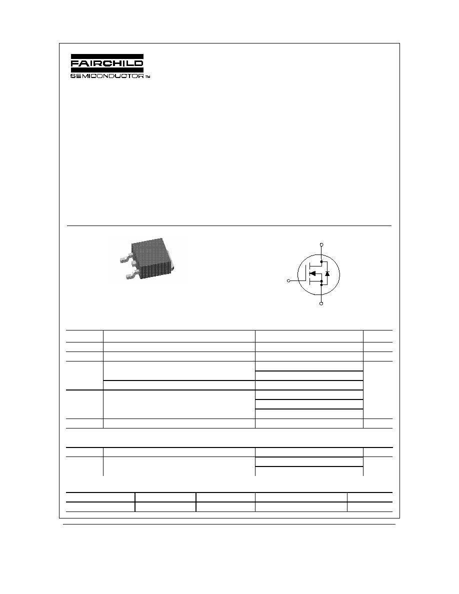
G
S
D
TO-252
S
D
G
Absolute Maximum Ratings
T
A
=25
o
C unless otherwise noted
Symbol
Parameter
Ratings
Units
V
DSS
Drain-Source Voltage
80
V
V
GSS
Gate-Source Voltage
±
20
V
Maximum Drain Current-Continuous
(Note 1)
43
(Note 1a)
10
I
D
Maximum Drain Current Pulsed
110
A
Maximum Power Dissipation @T
C
= 25
o
C
(Note 1)
69
T
A
= 25
o
C
(Note 1a)
3.4
P
D
T
A
= 25
o
C
(Note 1b)
1.3
W
T
J
, T
stg
Operating and Storage Junction Temperature Range
-55 to +150
°
C
Thermal Characteristics
R
JC
Thermal Resistance, Junction-to- Case
(Note 1)
1.8
°
C/W
R
JA
Thermal Resistance, Junction-to- Ambient
(Note 1a)
37
°
C/W
(Note 1b)
96
°
C/W
Package Marking and Ordering Information
Device Marking
Device
Reel Size
Tape width
Quantity
FDD3570
FDD3570
13''
16mm
2500
FDD3570
FDD3570 Rev. A(W)
Electrical Characteristics
T
A
= 25°C unless otherwise noted16
Symbol
Parameter
Test Conditions
Min Typ Max Units
Off Characteristics
BV
DSS
DrainSource Breakdown Voltage
V
GS
= 0 V, I
D
= 250
µ
A
80
V
BV
DSS
T
J
Breakdown Voltage Temperature
Coefficient
I
D
= 250
µ
A,Referenced to 25
°
C
78
mV/
°
C
I
DSS
Zero Gate Voltage Drain Current
V
DS
= 64 V,
V
GS
= 0 V
1
µ
A
I
GSSF
GateBody Leakage Current,
Forward
V
GS
= 20 V,
V
DS
= 0 V
100
nA
I
GSSR
GateBody Leakage Current,
Reverse
V
GS
= 20 V
V
DS
= 0 V
100
nA
On Characteristics
(Note 2)
V
GS(th)
Gate Threshold Voltage
V
DS
= V
GS
, I
D
= 250
µ
A
2
2.4
4
V
V
GS(th)
T
J
Gate Threshold Voltage
Temperature Coefficient
I
D
= 250
µ
A,Referenced to 25
°
C
-7
mV/
°
C
R
DS(on)
Static DrainSource
OnResistance
V
GS
= 10 V, I
D
= 10 A
V
GS
= 10 V, I
D
= 10 A,T
J
=125
°
C
V
GS
= 6 V, I
D
= 9 A
0.015
0.027
0.016
0.019
0.038
0.022
I
D(on)
OnState Drain Current
V
GS
= 10 V,
V
DS
= 5 V
25
A
g
FS
Forward Transconductance
V
DS
= 5 V,
I
D
= 14 A
40
S
Dynamic Characteristics
C
iss
Input Capacitance
2800
pF
C
oss
Output Capacitance
230
pF
C
rss
Reverse Transfer Capacitance
V
DS
= 40 V,
V
GS
= 0 V,
f = 1.0 MHz
117
pF
Switching Characteristics
(Note 2)
t
d(on)
TurnOn Delay Time
20
32
ns
t
r
TurnOn Rise Time
12
24
ns
t
d(off)
TurnOff Delay Time
60
95
ns
t
f
TurnOff Fall Time
V
DD
= 40 V,
I
D
= 1 A,
V
GS
= 10 V,
R
GEN
= 6
24
38
ns
Q
g
Total Gate Charge
54
76
nC
Q
gs
GateSource Charge
9.6
nC
Q
gd
GateDrain Charge
V
DS
= 40V,
I
D
= 9 A,
V
GS
= 10 V
14
nC
DrainSource Diode Characteristics and Maximum Ratings
I
S
Maximum Continuous DrainSource Diode Forward Current
2.8
A
V
SD
DrainSource Diode Forward
Voltage
V
GS
= 0 V,
I
S
= 2.8 A
(Note 2)
0.72
1.2
V
Notes:
1. R
JA
is the sum of the junction-to-case and case-to-ambient thermal resistance where the case thermal reference is defined as the solder mounting surface of
the drain pins. R
JC
is guaranteed by design while R
CA
is determined by the user's board design.
a) R
JA
= 40°/W when mounted on a
1in
2
pad of 2 oz copper
b) R
JA
= 96°/W when mounted on
a minimum pad.
Scale 1 : 1 on letter size paper
2. Pulse Test: Pulse Width < 300
µ
s, Duty Cycle < 2.0%
FDD3570
FDD3570 Rev. A(W)
Typical Characteristics
0
10
20
30
40
50
0
1
2
3
V
DS
, DRAIN-SOURCE VOLTAGE (V)
I
D
, DRAIN CURRENT (A)
6.0V
5.0V
4.5V
4.0V
3.5V
V
GS
= 10V
0.8
1
1.2
1.4
1.6
1.8
2
0
10
20
30
40
50
I
D
, DRAIN CURRENT (A)
R
DS(ON)
, NORMALIZED
DRAIN-SOURCE ON-RESISTANCE
V
GS
= 4.0V
6.0V
5.0V
7.0V
10V
4.5V
Figure 1. On-Region Characteristics.
Figure 2. On-Resistance Variation with
Drain Current and Gate Voltage.
0.4
0.6
0.8
1
1.2
1.4
1.6
1.8
2
-50
-25
0
25
50
75
100
125
150
T
J
, JUNCTION TEMPERATURE (
o
C)
R
DS(ON)
, NORMALIZED
DRAIN-SOURCE ON-RESISTANCE
I
D
= 9A
V
GS
= 10V
0
0.01
0.02
0.03
0.04
2
4
6
8
10
V
GS
, GATE TO SOURCE VOLTAGE (V)
R
DS(ON)
, ON-RESISTANCE (OHM)
I
D
= 10 A
T
A
= 125
o
C
T
A
= 25
o
C
Figure 3. On-Resistance Variation with
Temperature.
Figure 4. On-Resistance Variation with
Gate-to-Source Voltage.
0
10
20
30
40
50
2
3
4
5
6
V
GS
, GATE TO SOURCE VOLTAGE (V)
I
D
, DRAIN CURRENT (A)
T
A
= -55
o
C
25
o
C
125
o
C
V
DS
= 5V
0.0001
0.001
0.01
0.1
1
10
100
0
0.2
0.4
0.6
0.8
1
1.2
1.4
V
SD
, BODY DIODE FORWARD VOLTAGE (V)
I
S
, REVERSE DRAIN CURRENT (A)
T
A
= 125
o
C
25
o
C
-55
o
C
V
GS
= 0V
Figure 5. Transfer Characteristics.
Figure 6. Body Diode Forward Voltage Variation
with Source Current and Temperature.
FDD3570
FDD3570 Rev. A(W)
Typical Characteristics
0
2
4
6
8
10
0
10
20
30
40
50
60
Q
g
, GATE CHARGE (nC)
V
GS
, GATE-SOURCE VOLTAGE (V)
I
D
= 9A
V
DS
= 10V
40V
20V
0
500
1000
1500
2000
2500
3000
3500
4000
0
10
20
30
40
50
60
V
DS
, DRAIN TO SOURCE VOLTAGE (V)
CAPACITANCE (pF)
C
ISS
C
RSS
C
OSS
f = 1MHz
V
GS
= 0 V
Figure 7. Gate Charge Characteristics.
Figure 8. Capacitance Characteristics.
0.01
0.1
1
10
100
1000
0.1
1
10
100
V
DS
, DRAIN-SOURCE VOLTAGE (V)
I
D
, DRAIN CURRENT (A)
DC
10s
1s
100ms
100
µ
s
R
DS(ON)
LIMIT
V
GS
= 10V
SINGLE PULSE
R
JA
= 96
o
C/W
T
A
= 25
o
C
10ms
1ms
0
50
100
150
200
0.01
0.1
1
10
100
1000
t
1
, TIME (sec)
P(pk), PEAK TRANSIENT POWER (W)
SINGLE PULSE
R
JA
= 96 °C/W
T
A
= 25°C
Figure 9. Maximum Safe Operating Area.
Figure 10. Single Pulse Maximum
Power Dissipation.
0.001
0.01
0.1
1
0.0001
0.001
0.01
0.1
1
10
100
1000
t
1
, TIME (sec)
r(t), NORMALIZED EFFECTIVE TRANSIE
N
THERMAL RESISTANCE
R
JA
(t) = r(t) + R
JA
R
JA
= 96 °C/W
T
J
- T
A
= P * R
JA
(t)
Duty Cycle, D = t
1
/ t
2
P(pk)
t
1
t
2
SINGLE PULSE
0.01
0.02
0.05
0.1
0.2
D = 0.5
Figure 11. Transient Thermal Response Curve.
Thermal characterization performed using the conditions described in Note 1c.
Transient thermal response will change depending on the circuit board design.
FDD3570
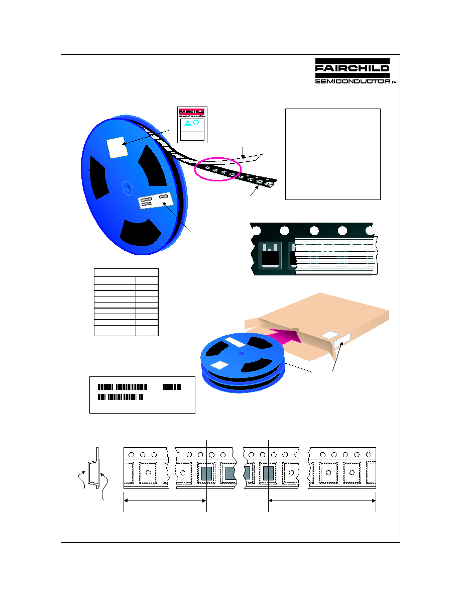
D-PAK (TO-252) Packaging
Configuration: Figure 1.0
Components
TO-252 (D-PAK) Tape Leader and
Trailer Configuration: Figure 2.0
Cover Tape
Carrier Tape
Note/Comments
Packaging Option
D-PAK (TO-252) Packaging Information
Standard
(no flow code)
Packaging type
Reel Size
TNR
13" Dia
Qty per Reel/Tube/Bag
2,500
Box Dimension (mm)
359x359x57
Max qty per Box
5,000
Weight per unit (gm)
0.300
Weight per Reel(kg)
1.200
ESD Label
F63TNR Label
359mm x 359mm x 57mm
Standard Intermediate box
D-PAK (TO-252) Unit Orientation
FDD
6680
FZ9
93
5
F63TNR Label sample
Static Dissipative
Embossed Carrier Tape
F63TNR
Label
Antistatic Cover Tape
ESD Label
EL ECT ROST AT IC
SEN SIT IVE DEVICES
DO NO T SHI P OR STO RE N EAR ST RO NG EL ECT ROST AT IC
EL ECT RO M AGN ETI C, M AG NET IC O R R ADIO ACT IVE FI ELD S
TNR DATE
PT NUMBER
PEEL STRENGTH MIN ______________gms
MAX _____________ gms
LOT: CBVK741B019
FSID: FDD6680
D/C1: Z9942 QTY1:
SPEC REV:
SPEC:
QTY: 2500
D/C2:
QTY2:
CPN:
N/F: F (F63TNR)3
Packaging Description:
TO-252 parts are shipped in tape. The carrier tape is
made from a dissipative (carbon filled) polycarbonate
resin. The cover tape is a multilayer film (Heat Activated
Adhesive in nature) primarily composed of polyester film,
adhesive layer, sealant, and anti-static sprayed agent.
These reeled parts in standard option are shipped with
2500 units per 13" or 330cm diameter reel. The reels are
dark blue in color and is made of polystyrene plastic (anti-
static coated). This and some other options are further
described in the Packaging Information table.
These full reels are individually barcode labeled and
placed inside a standard intermediate box (illustrated in
figure 1.0) made of recyclable corrugated brown paper.
One box contains two reels maximum. And these boxes
are placed inside a barcode labeled shipping box which
comes in different sizes depending on the number of parts
shipped.
FDD
6680
FZ9
93
5
FDD
6680
FZ9
93
5
FDD
6680
FZ9
93
5
Leader Tape
1680mm minimum or
210 empty pockets
Trailer Tape
640mm minimum or
80 empty pockets
TO-252 Tape and Reel Data and Package Dimensions
July 1999, Rev. A