May 2005
©
200
5 Fairchild Semiconductor Corporation
FDD6670AS Rev A(X)
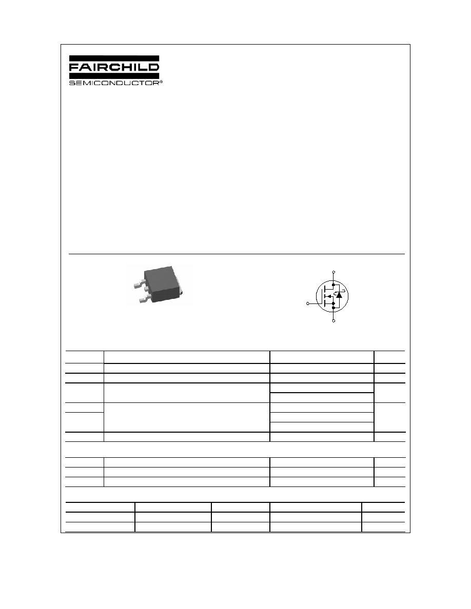
FDD6670AS
30V N-Channel PowerTrench
Æ
SyncFET
TM
General Description
The FDD6670AS is designed to replace a single
MOSFET and Schottky diode in synchronous DC:DC
power supplies. This 30V MOSFET is designed to
maximize power conversion efficiency, providing a low
R
DS(ON)
and low gate charge. The FDD6670AS
includes a patented combination of a MOSFET
monolithically integrated with a schottky diode. The
performance of the FDD6670AS as the low-side switch
in a synchronous rectifier is indistinguishable from the
performance of the FDD6670A in parallel with a
Schottky diode.
Applications
∑
DC/DC converter
∑
Low side notebook
Features
∑
76 A, 30 V
R
DS(ON)
max= 8.0 m
@ V
GS
= 10 V
R
DS(ON)
max= 10.4 m
@ V
GS
= 4.5 V
∑
Includes SyncFET Schottky body diode
∑
Low gate charge (29nC typical)
∑
High performance trench technology for extremely
low R
DS(ON)
∑
High power and current handling capability
.
G
S
D
TO-252
S
G
D
Absolute Maximum Ratings
T
A
=25
o
C unless otherwise noted
Symbol Parameter
Ratings
Units
V
DSS
Drain-Source
Voltage
30
V
V
GSS
Gate-Source
Voltage
±
20
V
Drain Current ≠ Continuous
(Note 3)
76
A
I
D
≠
Pulsed
(Note 1a)
100
P
D
Power Dissipation
(Note 1)
70
W
(Note 1a)
3.2
(Note 1b)
1.3
T
J
, T
STG
Operating and Storage Junction Temperature Range
≠55 to +150
∞
C
Thermal Characteristics
R
JC
Thermal Resistance, Junction-to-Case
(Note 1)
1.8
∞
C/W
R
JA
Thermal Resistance, Junction-to-Ambient
(Note 1a)
40
∞
C/W
R
JA
Thermal Resistance, Junction-to-Ambient
(Note 1b)
96
∞
C/W
Package Marking and Ordering Information
Device Marking
Device
Reel Size
Tape width
Quantity
FDD6670AS
FDD6670AS
13''
16mm
2500 units
FDD6670AS FDD6670AS_NL
(Note 4)
13''
16mm
2500 units
FDD6670
A
S
FDD6670AS Rev A (X)
Electrical Characteristics
T
A
= 25∞C unless otherwise noted
Symbol Parameter
Test
Conditions
Min Typ
Max
Units
Drain-Source Avalanche Ratings
(Note 2)
W
DSS
Drain-Source Avalanche Energy
Single Pulse, V
DD
= 15 V, I
D
=14A 245 mJ
I
AR
Drain-Source Avalanche Current
14
A
Off Characteristics
BV
DSS
Drain≠Source Breakdown Voltage
V
GS
= 0 V, I
D
= 1 mA
30
V
BV
DSS
T
J
Breakdown Voltage Temperature
Coefficient
I
D
= 10 mA, Referenced to 25
∞
C
29 mV/
∞
C
V
DS
= 24 V, V
GS
= 0 V
500
µ
A
I
DSS
Zero Gate Voltage Drain Current
V
DS
= 24 V, V
GS
= 0 V, T
J
= 125
∞
C
6.5 mA
I
GSS
Gate≠Body
Leakage
V
GS
=
±
20 V, V
DS
= 0 V
±
100
nA
On Characteristics
(Note 2)
V
GS(th)
Gate Threshold Voltage
V
DS
= V
GS
, I
D
= 1 mA
1
1.8
3
V
V
GS(th)
T
J
Gate Threshold Voltage
Temperature Coefficient
I
D
= 10 mA, Referenced to 25
∞
C
≠3.3
mV/
∞
C
R
DS(on)
Static Drain≠Source
On≠Resistance
V
GS
= 10 V,
I
D
= 13.8 A
V
GS
= 4.5 V,
I
D
= 11.7 A
V
GS
= 10 V, I
D
= 13.8A, T
J
= 125
∞
C
6.8
8.3
9.3
8.0
10.4
11.6
m
I
D(on)
On≠State Drain Current
V
GS
= 10 V,
V
DS
= 5 V
50
A
g
FS
Forward
Transconductance V
DS
= 15 V,
I
D
= 13.8 A
52
S
Dynamic Characteristics
C
iss
Input
Capacitance
1580
pF
C
oss
Output
Capacitance
440
pF
C
rss
Reverse Transfer Capacitance
V
DS
= 15 V,
V
GS
= 0 V,
f = 1.0 MHz
170 pF
R
G
Gate
Resistance
V
GS
= 15 mV, f = 1.0 MHz
1.8
Switching Characteristics
(Note 2)
t
d(on)
Turn≠On
Delay
Time
10
20
ns
t
r
Turn≠On Rise Time
12
22
ns
t
d(off)
Turn≠Off Delay Time
28
45
ns
t
f
Turn≠Off
Fall
Time
V
DS
= 15 V,
I
D
= 1 A,
V
GS
= 10 V,
R
GEN
= 6
20 36 ns
t
d(on)
Turn≠On
Delay
Time
15
27
ns
t
r
Turn≠On Rise Time
16
29
ns
t
d(off)
Turn≠Off Delay Time
26
42
ns
t
f
Turn≠Off
Fall
Time
V
DS
= 15 V,
I
D
= 1 A,
V
GS
= 4.5 V,
R
GEN
= 6
13 23 ns
Q
g(TOT)
Total Gate Charge at V
GS
=10V
29
40
nC
Q
g(TOT)
Total Gate Charge at V
GS
=5V
16
22
nC
Q
gs
Gate≠Source
Charge
4.6
nC
Q
gd
Gate≠Drain
Charge
V
DS
= 15 V, I
D
= 13.8 A,
5.5 nC
Drain≠Source Diode Characteristics
V
SD
Drain≠Source Diode Forward
Voltage
V
GS
= 0 V, I
S
= 3.5 A
(Note 2)
V
GS
= 0 V, I
S
= 7 A
(Note 2)
0.46
0.59
0.7 V
t
rr
Diode Reverse Recovery Time
20 n
s
Q
rr
Diode Reverse Recovery Charge
I
F
= 3.5 A,
d
iF
/d
t
= 300 A/µs
(Note
3)
15 nC
FDD6670
A
S
FDD6670AS Rev A (X)
D
R
P
DS(ON)
Electrical Characteristics
T
A
= 25∞C unless otherwise noted
Notes:
1. R
JA
is the sum of the junction-to-case and case-to-ambient thermal resistance where the case thermal reference is defined as the solder mounting surface of
the drain pins. R
JC
is guaranteed by design while R
CA
is determined by the user's board design.
a) R
JA
= 40∞C/W when mounted on a
1in
2
pad of 2 oz copper
b) R
JA
= 96∞C/W when mounted
on a minimum pad.
Scale 1 : 1 on letter size paper
2. Pulse Test: Pulse Width < 300
µ
s, Duty Cycle < 2.0%
3. Maximum current is calculated as:
where P
D
is maximum power dissipation at T
C
= 25∞C and R
DS(on)
is at T
J(max)
and V
GS
= 10V. Package current limitation is 21A
4. FDD6670AS_NL is a lead free product. The FDD6670AS_NL marking will appear on the reel label.
FDD6670
A
S
FDD6670AS Rev A (W)
Typical Characteristics
0
20
40
60
80
100
0
0.5
1
1.5
2
2.5
V
DS
, DRAIN-SOURCE VOLTAGE (V)
I
D
,
DRAI
N CU
RREN
T (
A
)
4.5V
4.0V
3.5V
V
GS
= 10V
6.0V
3.0V
2.5V
0.6
1
1.4
1.8
2.2
2.6
0
20
40
60
80
100
I
D
, DRAIN CURRENT (A)
R
DS
(
O
N)
,
NO
RMAL
I
Z
E
D
DRA
I
N
-
S
OU
RC
E
ON
-R
E
S
I
S
T
ANC
E
V
GS
= 3.0V
6.0V
10V
4.0V
4.5V
3.5V
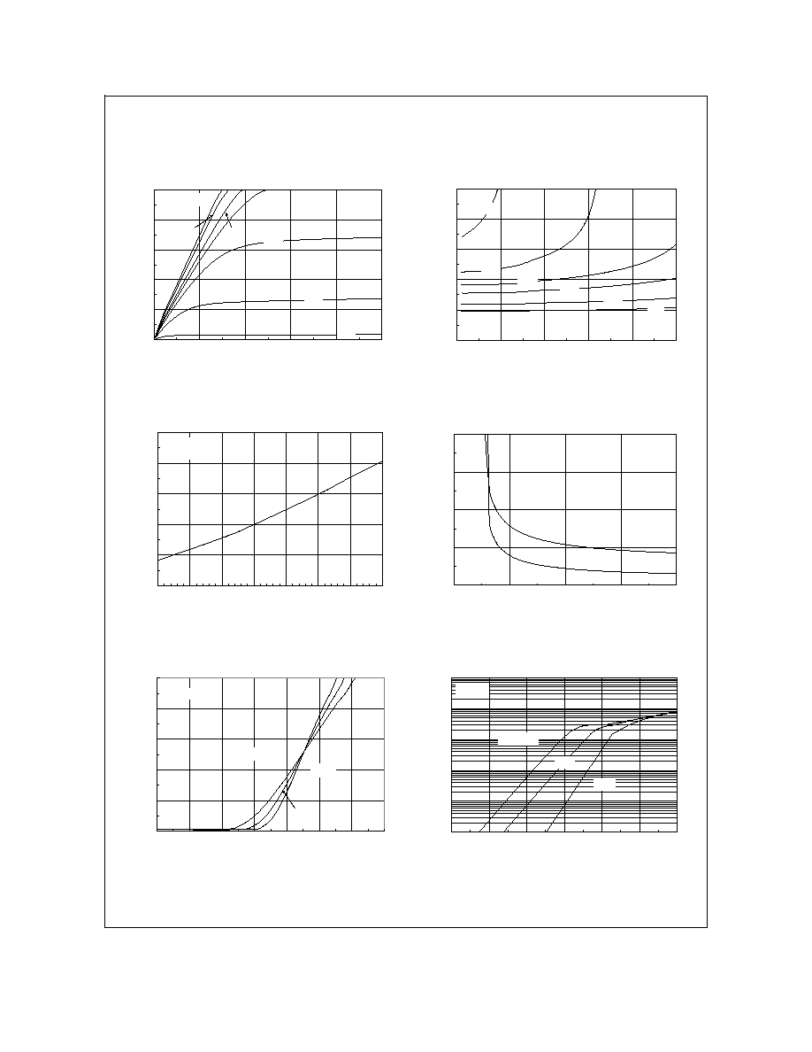
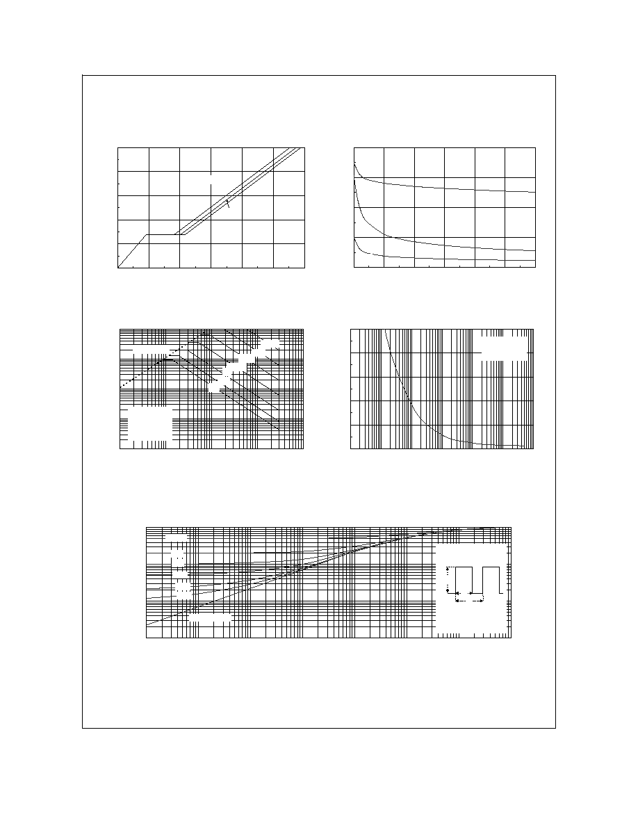
Figure 1. On-Region Characteristics.
Figure 2. On-Resistance Variation with
Drain Current and Gate Voltage.
0.6
0.8
1
1.2
1.4
1.6
-50
-25
0
25
50
75
100
125
T
J
, JUNCTION TEMPERATURE (
o
C)
R
DS
(
O
N)
,
NO
RMAL
I
Z
E
D
DR
AI
N-
S
O
URC
E
ON
-R
E
S
I
S
T
ANC
E
I
D
= 64A
V
GS
= 10V
0.005
0.01
0.015
0.02
0.025
2
4
6
8
10
V
GS
, GATE TO SOURCE VOLTAGE (V)
R
DS
(ON
)
, ON-
R
ESISTANCE (OHM
)
I
D
= 32A
T
A
= 125
o
C
T
A
= 25
o
C
Figure 3. On-Resistance Variation with
Temperature.
Figure 4. On-Resistance Variation with
Gate-to-Source Voltage.
0
20
40
60
80
100
1
1.5
2
2.5
3
3.5
4
4.5
V
GS
, GATE TO SOURCE VOLTAGE (V)
I
D
,
DR
AI
N CUR
RENT
(
A
)
T
A
= 125
o
C
25
o
C
-55
o
C
V
DS
= 5V
0.001
0.01
0.1
1
10
100
0
0.1
0.2
0.3
0.4
0.5
0.6
V
SD
, BODY DIODE FORWARD VOLTAGE (V)
I
S
,
R
E
V
E
RS
E DR
AI
N CU
RR
ENT
(A
)
T
A
= 125
o
C
25
o
C
-55
o
C
V
GS
= 0V
Figure 5. Transfer Characteristics.
Figure 6. Body Diode Forward Voltage Variation
with Source Current and Temperature.
FDD6670
A
S
FDD6670AS Rev A (W)
Typical Characteristics
(continued)
0
2
4
6
8
10
0
5
10
15
20
25
30
Q
g
, GATE CHARGE (nC)
V
GS
, GA
TE-
S
OU
RC
E VOL
T
AG
E (V)
I
D
=13.8A
V
DS
= 10V
15V
20V
0
600
1200
1800
2400
0
5
10
15
20
25
30
V
DS
, DRAIN TO SOURCE VOLTAGE (V)
CA
P
ACI
TA
NC
E
(p
F
)
C
iss
C
rss
C
oss
f = 1MHz
V
GS
= 0 V
Figure 7. Gate Charge Characteristics.
Figure 8. Capacitance Characteristics.
0.01
0.1
1
10
100
0.01
0.1
1
10
100
V
DS
, DRAIN-SOURCE VOLTAGE (V)
I
D
,
DRAI
N C
URRE
NT
(A
)
DC
10s
1s
100ms
100
µ
s
R
DS(ON)
LIMIT
V
GS
= 10V
SINGLE PULSE
R
JA
= 96
o
C/W
T
A
= 25
o
C
10ms
1ms
0
10
20
30
40
50
0.001
0.01
0.1
1
10
100
1000
t
1
, TIME (sec)
P(
pk), PEA
K TR
A
N
SIEN
T POWER
(W)
SINGLE PULSE
R
JA
= 96∞C/W
T
A
= 25∞C
Figure 9. Maximum Safe Operating Area.
Figure 10. Single Pulse Maximum
Power Dissipation.
0.001
0.01
0.1
1
0.0001
0.001
0.01
0.1
1
10
100
1000
t
1
, TIME (sec)
r
(
t
)
,
NO
RM
A
L
I
Z
E
D
EF
F
E
CT
I
V
E
T
RANS
I
E
N
T
T
H
ER
M
A
L
R
E
SI
S
T
ANC
E
R
JA
(t) = r(t) * R
JA
R
JA
= 96 ∞C/W
T
J
- T
A
= P * R
JA
(t)
Duty Cycle, D = t
1
/ t
2
P(pk)
t
1
t
2
SINGLE PULSE
0.01
0.02
0.05
0.1
0.2
D = 0.5
Figure 11. Transient Thermal Response Curve.
Thermal characterization performed using the conditions described in Note 1c.
Transient thermal response will change depending on the circuit board design.
FDD6670
A
S
FDD6670AS Rev A (W)
Typical Characteristics
(continued)
SyncFET Schottky Body Diode
Characteristics
Fairchild's SyncFET process embeds a Schottky diode
in parallel with PowerTrench MOSFET. This diode
exhibits similar characteristics to a discrete external
Schottky diode in parallel with a MOSFET. Figure 12
shows the reverse recovery characteristic of the
FDD6670AS.
Figure 12. FDD6670AS SyncFET body diode
reverse recovery characteristic.
For comparison purposes, Figure 13 shows the reverse
recovery characteristics of the body diode of an
equivalent size MOSFET produced without SyncFET
(FDD6670A).
Figure 13. Non-SyncFET (FDD6670A) body
diode reverse recovery characteristic.
Schottky barrier diodes exhibit significant leakage at
high temperature and high reverse voltage. This will
increase the power in the device.
0.00001
0.0001
0.001
0.01
0.1
0
10
20
30
V
DS
, REVERSE VOLTAGE (V)
I
DSS
,
REVER
S
E
LE
A
K
AGE CU
RRENT (
A
)
100
o
C
25
o
C
125
o
C
Figure 14. SyncFET body diode reverse
leakage versus drain-source voltage and
temperature.
FDD6670
A
S
TIME : 12.5ns/div
CURRE
NT : 0
.
8
A
/div
TIME : 12.5ns/div
CURRE
NT : 0
.
8
A
/div
DISCLAIMER
FAIRCHILD SEMICONDUCTOR RESERVES THE RIGHT TO MAKE CHANGES WITHOUT FURTHER NOTICE TO ANY
PRODUCTS HEREIN TO IMPROVE RELIABILITY, FUNCTION OR DESIGN. FAIRCHILD DOES NOT ASSUME ANY LIABILITY
ARISING OUT OF THE APPLICATION OR USE OF ANY PRODUCT OR CIRCUIT DESCRIBED HEREIN; NEITHER DOES IT
CONVEY ANY LICENSE UNDER ITS PATENT RIGHTS, NOR THE RIGHTS OF OTHERS.
TRADEMARKS
The following are registered and unregistered trademarks Fairchild Semiconductor owns or is authorized to use and is
not intended to be an exhaustive list of all such trademarks.
LIFE SUPPORT POLICY
FAIRCHILD'S PRODUCTS ARE NOT AUTHORIZED FOR USE AS CRITICAL COMPONENTS IN LIFE SUPPORT
DEVICES OR SYSTEMS WITHOUT THE EXPRESS WRITTEN APPROVAL OF FAIRCHILD SEMICONDUCTOR CORPORATION.
As used herein:
1. Life support devices or systems are devices or
systems which, (a) are intended for surgical implant into
the body, or (b) support or sustain life, or (c) whose
failure to perform when properly used in accordance
with instructions for use provided in the labeling, can be
reasonably expected to result in significant injury to the
user.
2. A critical component is any component of a life
support device or system whose failure to perform can
be reasonably expected to cause the failure of the life
support device or system, or to affect its safety or
effectiveness.
PRODUCT STATUS DEFINITIONS
Definition of Terms
Datasheet Identification
Product Status
Definition
Advance Information
Preliminary
No Identification Needed
Obsolete
This datasheet contains the design specifications for
product development. Specifications may change in
any manner without notice.
This datasheet contains preliminary data, and
supplementary data will be published at a later date.
Fairchild Semiconductor reserves the right to make
changes at any time without notice in order to improve
design.
This datasheet contains final specifications. Fairchild
Semiconductor reserves the right to make changes at
any time without notice in order to improve design.
This datasheet contains specifications on a product
that has been discontinued by Fairchild semiconductor.
The datasheet is printed for reference information only.
Formative or
In Design
First Production
Full Production
Not In Production
IntelliMAXTM
ISOPLANARTM
LittleFETTM
MICROCOUPLERTM
MicroFETTM
MicroPakTM
MICROWIRETM
MSXTM
MSXProTM
OCXTM
OCXProTM
OPTOLOGIC
OPTOPLANARTM
PACMANTM
FAST
FASTrTM
FPSTM
FRFETTM
GlobalOptoisolatorTM
GTOTM
HiSeCTM
I
2
CTM
i-LoTM
ImpliedDisconnectTM
Rev. I15
ACExTM
ActiveArrayTM
BottomlessTM
CoolFETTM
CROSSVOLTTM
DOMETM
EcoSPARKTM
E
2
CMOSTM
EnSignaTM
FACTTM
FACT Quiet SeriesTM
POPTM
Power247TM
PowerEdgeTM
PowerSaverTM
PowerTrench
QFET
QSTM
QT OptoelectronicsTM
Quiet SeriesTM
RapidConfigureTM
RapidConnectTM
µ
SerDesTM
SILENT SWITCHER
SMART STARTTM
SPMTM
StealthTM
SuperFETTM
SuperSOTTM-3
SuperSOTTM-6
SuperSOTTM-8
SyncFETTM
TinyLogic
TINYOPTOTM
TruTranslationTM
UHCTM
UltraFET
UniFETTM
VCXTM
Across the board. Around the world.TM
The Power Franchise
Programmable Active DroopTM