 | –≠–ª–µ–∫—Ç—Ä–æ–Ω–Ω—ã–π –∫–æ–º–ø–æ–Ω–µ–Ω—Ç: FDFM2N111 | –°–∫–∞—á–∞—Ç—å:  PDF PDF  ZIP ZIP |
August 2005
F
D
FM2N111 Integ
r
ated N-Chan
nel PowerTrench
Æ
MOSFET and Schottky Diode
©2005 Fairchild Semiconductor Corporation FDFM2N111 Rev. C2 (W)
1
FDFM2N111
Integrated N-Channel PowerTrench
Æ
MOSFET and Schottky Diode
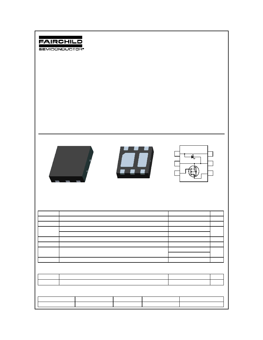
General Description
FDFM2N111 combines the exceptional performance of
Fairchild's PowerTrench MOSFET technology with a very
low forward voltage drop Schottky barrier rectifier in a
MicroFET package.
This device is designed specifically as a single package
solution for Standard Buck Converter. It features a fast
switching, low gate charge MOSFET with very low on-state
resistance.
Applications
Standard Buck Converter
Features
4 A, 20 V R
DS(ON)
= 100m
@ V
GS
= 4.5 V
R
DS(ON)
= 150m
@ V
GS
= 2.5 V
Low Profile - 0.8 mm maximun - in the new package
MicroFET 3x3 mm
Absolute Maximum Ratings
T
A
= 25∞C unless otherwise noted
Thermal Characteristics
Package Marking and Ordering Information
Symbol
Parameter
Ratings
Units
V
DSS
Drain-Source Voltage
20
V
V
GSS
Gate-Source Voltage
±12
V
I
D
Drain Current -Continuous (Note 1a)
4
A
-Pulsed
10
V
RRM
Schottky Repetitive Peak Reverse voltage
20
V
I
O
Schottky Average Forward Current (Note 1a)
2
A
P
D
Power dissipation (Steady State) (Note 1a)
Power dissipation (Steady State) (Note 1b)
1.7
W
0.8
T
J
, T
STG
Operating and Storage Junction Temperature Range
-55 to +150
o
C
R
JA
Thermal Resistance, Junction-to-Ambient (Note 1a)
70
o
C/W
R
JA
Thermal Resistance, Junction-to-Ambient (Note 1b)
150
o
C/W
Device Marking
Device
Reel Size
Tape Width
Quantity
2N111
FDFM2N111
7inch
12mm
3000 units
5
1
6
2
3
4
MLP 3x3
TOP
BOTTOM
A
A
S/C
S/C G
D
PIN 1
A
S/C
D
A
S/C
G
C
D

F
D
FM2N111 Integ
r
ated N-Chan
nel PowerTrench
Æ
MOSFET and Schottky Diode
FDFM2N111 Rev. C2 (W)
2
Electrical Characteristics
T
A
= 25∞C unless otherwise noted
Symbol
Parameter
Test Conditions
Min
Typ
Max
Units
Off Characteristics
B
VDSS
Drain-Source Breakdown Voltage
I
D
= 250
µA, V
GS
= 0V
20
-
-
V
BV
DSS
T
J
Breakdown Voltage Temperature
Coefficient
I
D
= 250
µA,
Referenced to 25∞C
-
12
-
mV/∞C
I
DSS
Zero Gate Voltage Drain Current
V
GS
= 0V, V
DS
= 16V
-
-
1
µA
I
GSS
Gate-Body Leakage,
V
GS
=
±12V, V
DS
= 0V
-
-
±100
nA
On Characteristics
V
GS(TH)
Gate Threshold Voltage
V
DS
= V
GS
, I
D
= 250
µA
0.6
1.0
1.5
V
V
GS(TH)
T
J
Gate Threshold Voltage
Temperature Coefficient
I
D
= 250
µA,
Referenced to 25∞C
-
-3
-
mV/∞C
R
DS(ON)
Static Drain-Source On-Resistance
I
D
= 4.0A, V
GS
= 4.5V
-
54
100
m
I
D
= 3.3A, V
GS
= 2.5V
-
83
150
I
D
= 4.0A, V
GS
= 4.5V,
T
J
= 125∞C
-
74
147
I
D(ON)
On-State Drain Current
V
GS
= 2.5V, V
DS
= 5V
10
-
-
A
g
FS
Forward Transconductance
I
D
= 4A, V
DS
= 5V
-
9.7
-
S
(Note 2)
Dynamic Characteristics
C
ISS
Input Capacitance
V
DS
= 10V, V
GS
= 0V,
f = 1MHz
-
273
-
pF
C
OSS
Output Capacitance
-
63
-
pF
C
RSS
Reverse Transfer Capacitance
-
37
-
pF
R
G
Gate Resistance
V
GS
= 0V, f = 1MHz,
-
1.6
-
Switching Characteristics
(Note 2)
t
d(ON)
Turn-On Delay Time
V
DD
= 10V, I
D
= 1A
V
GS
= 4.5V, R
GEN
= 6
-
6
12
ns
t
r
Turn-On Rise Time
-
7
14
ns
t
d(OFF)
Turn-Off Delay Time
-
11
20
ns
t
f
Turn-Off Fall Time
-
1.7
3.4
ns
Q
g
Total Gate Charge
V
DS
= 10V, I
D
= 4.0A,
V
GS
= 4.5V
-
2.7
3.8
nC
Q
gs
Gate-Source Charge
-
0.6
-
nC
Q
gd
Gate-Drain Charge
-
0.9
-
nC
Drain-Source Diode Characteristics and Maximum Ratings
I
S
Maximum Continuous Drain-Source Diode Forward Current
-
-
1.4
A
V
SD
Drain-Source Diode Forward Voltage
V
GS
= 0V, I
S
= 1.4 A (Note 2)
-
0.8
-1.2
V
t
rr
Diode Reverse Recovery Time
I
F
= 4.0A, dI
F
/dt=100A/
µs
-
11
-
ns
Q
rr
Diode Reverse Recovery Charge
-
3
-
nC
Schottky Diode Characteristic
V
R
Reverse Voltage
I
R
= 1mA
20
-
-
V
I
R
Reverse Leakage
V
R
= 5V
T
J
= 25∞C
-
-
100
µA
T
J
= 100∞C
10
mA
V
F
Forward Voltage
I
F
= 1A
T
J
= 25∞C
-
0.32
0.39
V

F
D
FM2N111 Integ
r
ated N-Chan
nel PowerTrench
Æ
MOSFET and Schottky Diode
FDFM2N111 Rev. C2 (W)
3
Electrical Characteristics
T
A
= 25∞C unless otherwise noted
Notes:
1. R
JA
is the sum of the junction-to-case and case-to-ambient thermal resistance where the case thermal reference is
defined as the solder mounting surface of the drain pins. R
CA
is guaranteed by design while R
CA
is determined by the
user's board design.
a) 70
o
C/W when mounted on
a 1in
2
pad of 2 oz copper
b) 150
o
C/W whe mounted on
a minimum pad of 2 oz
copper
Scale 1: 1 on letter size paper
2. Pulse Test: Pulse Width < 300
µs, Duty Cycle < 2.0%
F
D
FM2N111 Integ
r
ated N-Chan
nel PowerTrench
Æ
MOSFET and Schottky Diode
FDFM2N111 Rev. C2 (W)
4
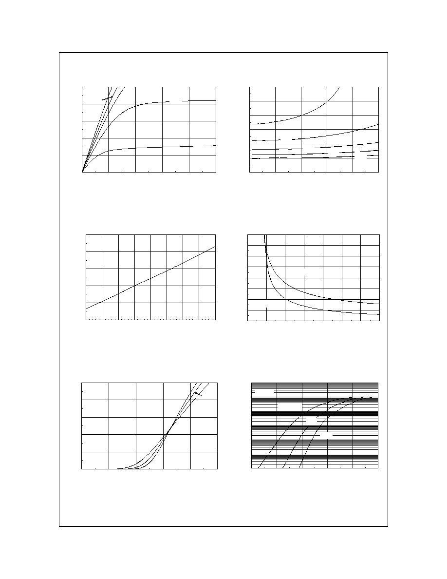
Typical Characteristics
Figure 1.
0
2
4
6
8
10
0
0.5
1
1.5
2
2.5
V
DS
, DRAIN-SOURCE VOLTAGE (V)
I
D
,
D
RAI
N CUR
RENT
(
A)
2.5V
2.0V
V
GS
= 4.5V
3.0V
3.5V
On-Region Characteristics
Figure 2.
0.8
1
1.2
1.4
1.6
1.8
2
0
2
4
6
8
10
I
D
, DRAIN CURRENT (A)
R
DS
(
O
N)
,
NORM
A
L
I
Z
E
D
DRA
I
N
-
S
OURC
E
ON
-
R
E
S
I
S
T
A
NCE
V
GS
= 2.5V
4.0V
3.5V
4.5V
3.0V
On-Resistance Variation with
Drain Current and Gate Voltage
Figure 3.
0.6
0.8
1
1.2
1.4
1.6
-50
-25
0
25
50
75
100
125
150
T
J
, JUNCTION TEMPERATURE (
o
C)
R
DS
(
O
N)
,
NO
R
M
AL
I
Z
ED
D
RAI
N-
S
O
U
RCE
ON-
R
E
S
I
S
TA
NCE
I
D
= 4A
V
GS
= 4.5V
On-Resistance Variation with
Temperature
Figure 4.
0.04
0.06
0.08
0.1
0.12
0.14
0.16
0.18
0.2
1.5
2
2.5
3
3.5
4
4.5
5
V
GS
, GATE TO SOURCE VOLTAGE (V)
R
DS
(
O
N)
, O
N
-
R
E
S
IS
T
A
N
C
E
(
O
H
M
)
I
D
= 2A
T
A
= 125
o
C
T
A
= 25
o
C
On-Resistance Variation with
Gate-to-Source Voltage
Figure 5. Transfer Characteristics
0
2
4
6
8
10
0.5
1
1.5
2
2.5
3
V
GS
, GATE TO SOURCE VOLTAGE (V)
I
D
,
DR
AI
N
CU
RR
EN
T
(
A
)
T
A
= -55
o
C
25
o
C
125
o
C
V
DS
= 5V
Figure 6.
0.0001
0.001
0.01
0.1
1
10
100
0.2
0.4
0.6
0.8
1
1.2
-V
SD
, BODY DIODE FORWARD VOLTAGE (V)
-I
S
,
R
E
VE
RS
E
DR
A
I
N
CU
RR
E
N
T
(
A)
T
A
= 125
o
C
25
o
C
-55
o
C
V
GS
= 0V
Body Diode Forward Voltage Variation
with Source Current and Temperature

F
D
FM2N111 Integ
r
ated N-Chan
nel PowerTrench
Æ
MOSFET and Schottky Diode
FDFM2N111 Rev. C2(W)
5
Figure 7.
0
1
2
3
4
5
6
0
1
2
3
4
Q
g
, GATE CHARGE (nC)
V
GS
,
G
A
TE-
S
OU
R
C
E
VO
LTA
G
E
(
V)
I
D
= 4A
V
DS
= 5V
15V
10V
Gate Charge Characteristics
Figure 8.
0
50
100
150
200
250
300
350
400
0
4
8
12
16
20
V
DS
, DRAIN TO SOURCE VOLTAGE (V)
CA
PACI
T
AN
CE (
p
F
)
C
iss
C
rss
C
oss
f = 1MHz
V
GS
= 0 V
Capacitance Characteristics
Figure 9.
0.001
0.01
0.1
1
10
0
0.1
0.2
0.3
0.4
0.5
0.6
0.7
0.8
V
F
, FORWARD VOLTAGE (V)
I
F
,
F
O
RW
ARD
L
E
AKAG
E
CUR
RE
NT
(
A)
T
J
= 25
o
C
T
J
= 125
o
C
Schottky Diode Forward Voltage
Figure 10.
0.000001
0.00001
0.0001
0.001
0.01
0.1
0
5
10
15
20
V
R
, REVERSE VOLTAGE (V)
I
R
,
R
E
V
E
RS
E
L
E
AKAGE
CU
RRE
NT
(
A)
T
J
= 25
o
C
T
J
= 125
o
C
T
J
= 100
o
C
Schottky Diode Reverse Current
Figure 11. Transient Thermal Response Curve
Thermal characterization performed using the conditions described in Note 1b.
Transient thermal response will change depending on the circuit board design.
Typical Characteristics