 | ÐлекÑÑоннÑй компоненÑ: FDG901D | СкаÑаÑÑ:  PDF PDF  ZIP ZIP |
Äîêóìåíòàöèÿ è îïèñàíèÿ www.docs.chipfind.ru
April 2002
2002 Fairchild Semiconductor Corporation
FDG901D rev. E (W)
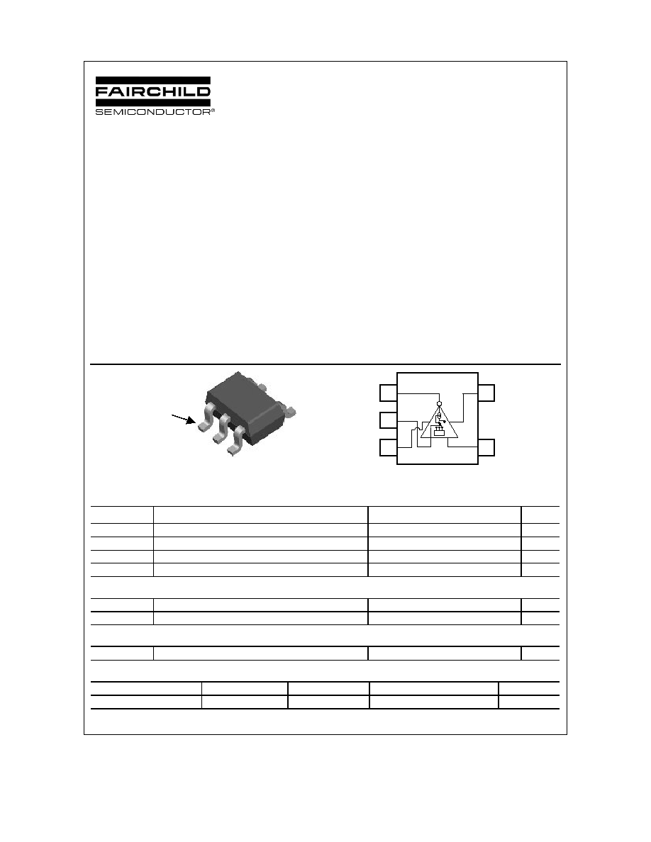
FDG901D
Slew Rate Control Driver IC for P-Channel MOSFETs
General Description
The FDG901D is specifically designed to control the
turn on of a P-Channel MOSFET in order to limit the
inrush current in battery switching applications with high
capacitance loads. During turn-on the FDG901D drives
the MOSFET's gate low with a regulated current
source, thereby controlling the MOSFET's turn on. For
turn-off, the IC pulls the MOSFET gate up quickly, for
efficient turn off.
Applications
· Power management
· Battery Load switch
Features
· Three Programmable slew rates
· Reduces inrush current
· Minimizes EMI
· Normal turn-off speed
· Low-Power CMOS operates over wide voltage range
· Compact industry standard SC70-5 surface mount
package
pin 1
LOGIC IN
5
4
1
2
3
GND
GATE
SLEW
VDD
Absolute Maximum Ratings
T
A
=25
o
C unless otherwise noted
Symbol Parameter
Ratings
Units
V
DD
Supply Voltage
-0.5 to 10
V
V
IN
DC Input Voltage (Logic Inputs)
-0.7 to 6
V
P
D
Power Dissipation for Single Operation @ 85°C
150
mW
T
J
, T
STG
Operating and Storage Junction Temperature Range
-65 to +150
°C
Recommended Operating Range
V
DD
Supply Voltage
2.7 to 6.0
V
T
J
Operating Temperature
-40 to +125
°C
Thermal Characteristics
R
JA
Thermal Resistance, Junction-to-Ambient
(Note 1)
425
°C/W
Package Marking and Ordering Information
Device Marking
Device
Reel Size
Tape width
Quantity
91
FDG901D
7''
8mm
3000 units
FDG901D
FDG901D rev. D (W)
Electrical Characteristics
T
A
= 25°C unless otherwise noted
Symbol Parameter
Test
Conditions
Min
Typ
Max
Units
Logic Levels
V
IH
Logic HIGH Input Voltage
V
DD
= 2.70V to 6.0 V
75%
of V
DD
V
V
IL
Logic LOW Input Voltage
V
DD
= 2.70V to 6.0 V
25%
of V
DD
V
OFF Characteristics
BV
IN
Logic Input Breakdown Voltage
I
IN
= 10
µA, V
SLEW
= 0 V
9 V
BV
SLEW
Slew Input Breakdown Voltage
I
SLEW
= 10
µA, V
IN
= 0 V
9 V
BV
DG
Supply Input Breakdown Voltage
I
DG
= 10
µA, V
IN
= 0 V, V
SLEW
= 0 V
9 V
I
RIN
LOGIC Input Leakage Current
V
IN
= 8 V, V
SLEW
= 0 V
100
nA
I
RSLEW
SLEW Input Leakage Current
V
SLEW
= 8 V, V
IN
= 0 V
100
nA
I
RDG
Supply Input Leakage Current
V
DG
= 8 V, V
IN
= 0 V, V
SLEW
= 0 V
100
nA
ON Characteristics
I
G
Gate Current
SLEW = OPEN
90
120
µA
SLEW = GND
1
10
µA
V
IN
= 6V
V
GATE
= 2V
SLEW = V
DD
10
50
nA
Switching Characteristics
t
don
Output Turn-On Delay Time
Slew Pin = OPEN
8.3 µs
t
don
Output Turn-On Delay Time
Slew Pin = GROUND
0.6 ms
t
don
Output Turn-On Delay Time
Slew Pin = VDD
V
Supply
= 5.5 V, V
DD
= 5.5 V,
Logic IN = 5.5 V,
C
LOAD
= 510 pF, Test Circuit
2.2 ms
t
rise
Output Rise Time
Slew Pin = OPEN
28 µs
t
rise
Output Rise Time
Slew Pin = GROUND
1.8 ms
t
rise
Output Rise Time
Slew Pin = VDD
V
Supply
= 5.5 V, V
DD
= 5.5 V,
Logic IN = 5.5 V,
C
LOAD
= 510 pF, Test Circuit
11 ms
dv/dt Output
Slew
Rate
Slew Pin = OPEN
162 V/ms
dv/dt Output
Slew
Rate
Slew Pin = GROUND
2.6 V/ms
dv/dt Output
Slew
Rate
Slew Pin = VDD
V
Supply
= 5.5 V, V
DD
= 5.5 V,
Logic IN = 5.5 V,
C
LOAD
= 510 pF, Test Circuit
0.3 V/ms
Notes: R
JA
is the sum of the junction-to-case and case-to-ambient thermal resistance where the case thermal reference is defined as the solder mounting surface
of the drain pins. R
JC
is guaranteed by design while R
CA
is determined by the user's board design.
FDG901D
LOGIC IN
VDD
SLEW
V
SUPPLY
C
Load
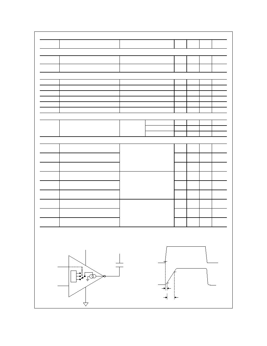
Test Circuit
1
2
4
3
5
LOGIC IN
VDD
SLEW
V
SUPPLY
C
Load
Test Circuit
1
2
4
3
5
tdon
trise
10%
10%
90%
LOGIC IN
OUTPUT
(Inverted)
Switching Waveforms
tdon
trise
10%
10%
90%
LOGIC IN
OUTPUT
(Inverted)
Switching Waveforms
FDG901D rev. D (W)
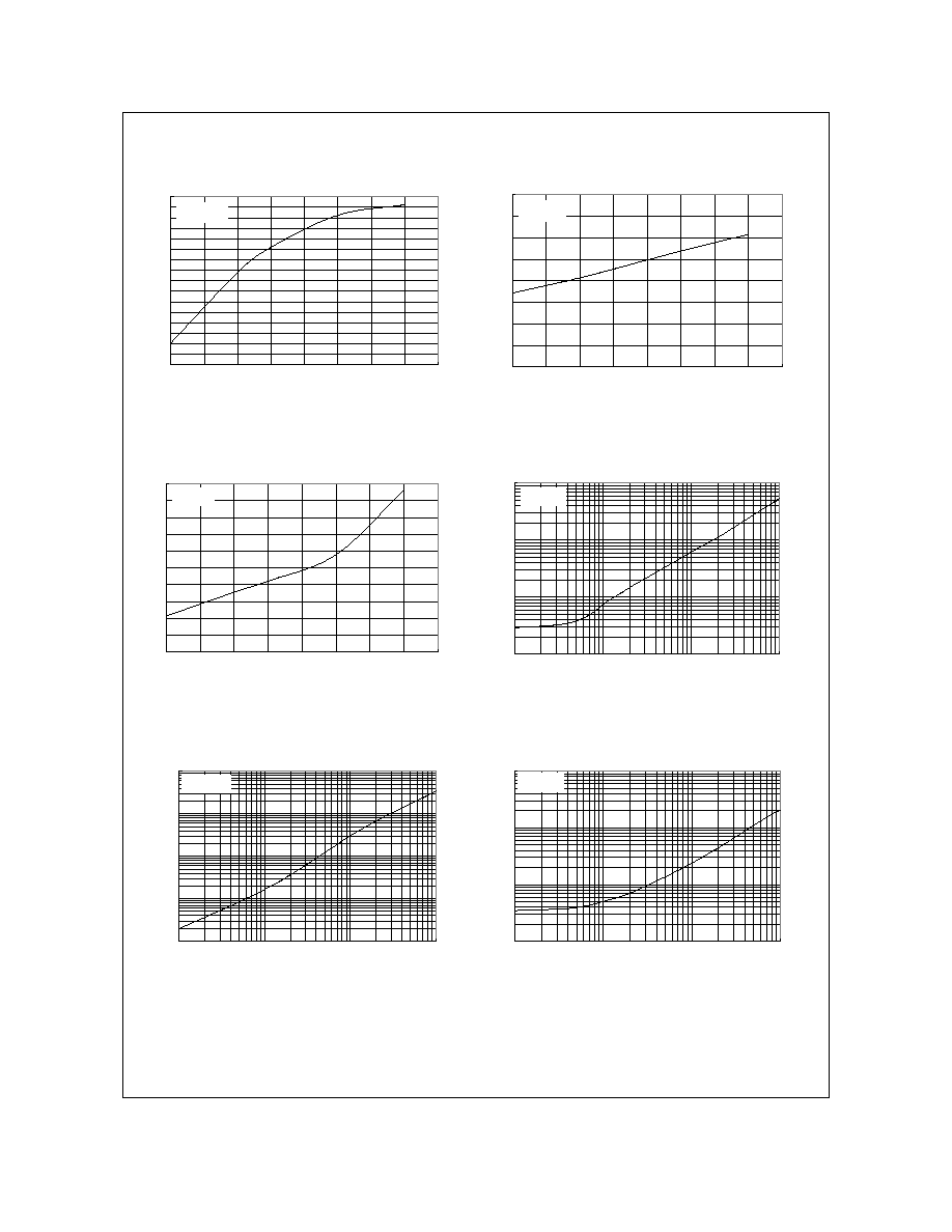
Typical Characteristics
Figure 1. GATE Output current vs.
Temperature. SLEW = OPEN
Figure 2. GATE Output current vs.
Temperature. SLEW = Ground
Figure 3. GATE Output current vs.
Temperature. SLEW = V
DD
Figure 4. t
rise
vs. Load Capacitance.
SLEW = OPEN
Figure 5. t
rise
vs. Load Capacitance.
SLEW = GROUND
Figure 6. t
rise
vs. Load Capacitance.
SLEW = V
DD
FDG901D
0.0
0.5
1.0
1.5
2.0
-50
0
50
100
150
Temperature, (
o
C)
G
a
te
Cu
r
r
e
n
t
(
µ
A)
Slew = Gnd
Vdd=Vin=6V
60
65
70
75
80
85
90
95
100
-50
0
50
100
150
Temperature, (
o
C)
G
a
te
Cu
r
r
e
n
t, (
µ
A)
Slew = Open
Vdd=Vin=6V
4
6
8
10
12
14
-50
0
50
100
150
Temperature, (
o
C)
G
a
te
Cu
r
r
e
n
t, (
n
A
)
Slew = Vdd
Vdd=Vin=6V
0.1
1
10
100
1
10
100
1000
Load Capacitance, picoFarad (pF)
Out
put
R
i
s
e
t
i
m
e
,
m
i
c
r
os
ec
onds
(
µ
se
c)
Slew = Open
Vdd=Vin=5.5V
0.1
1
10
100
1
10
100
1000
Load Capacitance, picoFarad (pF)
Out
put
R
i
s
e
t
i
m
e
,
m
illis
ec
onds
(m
s
)
Slew = Vdd
Vdd=Vin=5.5V
1
10
100
1000
10000
1
10
100
1000
Load Capacitance, picoFarad (pF)
Out
put
R
i
s
e
t
i
m
e
,
m
i
c
r
os
ec
onds
(
µ
s)
Slew = Gnd
Vdd=Vin=5.5V
FDG901D rev. D (W)
Typical Application
Battery powered systems make extensive usage of load switching, turning the power to
subsystems off, in order to extend battery life. Power MOSFETs are used to accomplish this
task. In PDA's and Cell phones, these MOSFETs are usually low threshold P-Channels. Since
the loads typically include bypass capacitor components (high capacitive component), a high
inrush current can occur when the load is switched on. This inrush current can cause transients
on the main power supply disturbing circuitry supplied by it.
The simplest method of limiting the inrush current is to control the slew rate of the MOSFET
switch. This can be done with external R/C circuits, but this approach can occupy significant PCB
area, and involves other compromises in performance. The slew rate control driver IC FDG901D
is specifically designed to interface low voltage digital circuitry with power MOSFETs and reduce
the rapid inrush current in load switch applications. The IC limits inrush current by controlling the
current, which drives the gate of the P-Channel MOSFET switch.
The control input is a CMOS compatible input with a minimum high input voltage of 2.55V with a
power rail voltage of 6V. Therefore, it is compatible with any CMOS logic voltages between
2.55V and 5V and under these conditions there is no additional configuration required.
Load
Ig
Application Circuit
1
3
5
4
2
Slew Rate
Control
Logic
Signal
I
Source
Gate
Drain
VDD
FDG901D rev. D (W)
The Slew Rate Control Driver (FDG901D) is designed to give a programmed choice of one of
three steady dv/dt states on the output during turn-on. To change the dv/dt value, the user needs
to use the Slew Rate Control Pin (Pin 2). To utilize the smallest current setting (
10 nA) from the
IC, a voltage equal to Vdd must be applied to the Slew Rate Control Pin 2. To use the next
higher current setting (
1 µA) a voltage equal to Ground must be applied to Pin 2. To achieve the
highest current setting (
80 µA) or obtain a faster switching speed, the Slew Rate Pin2 must be
open (floating). A higher value of capacitance will result in a slower switching rate. To determine
the switching times of each setting use the simple equation:
G
g
I
Q
t
=
where Q
g
is the Gate charge in nC for a given MOSFET and I
G
is the gate current controlled by
the slew rate pin.
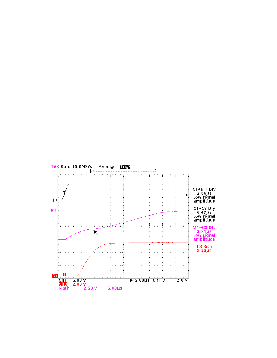
Below is a captured image from an oscilloscope depicting the device response. The FDG901D
was connected to control an FDG258P P-Channel DMOS. The Slew Rate control pin was set to
open (floating state).
V
IN
= 5.5V
V
DD
= 5.5V
R
LOAD
= 1.5
Test Conditions:
V
IN
= 5.5V
V
DD
= 5.5V
R
LOAD
= 1.5
Test Conditions:
V
RLoad
V
gate
(inverted)
V
IN
Circuit waveforms for an FDG901D controlling a P-Channel FDG258P MOSFET.
V
RLoad
V
gate
(inverted)
V
IN
Circuit waveforms for an FDG901D controlling a P-Channel FDG258P MOSFET.

DISCLAIMER
FAIRCHILD SEMICONDUCTOR RESERVES THE RIGHT TO MAKE CHANGES WITHOUT FURTHER
NOTICE TO ANY PRODUCTS HEREIN TO IMPROVE RELIABILITY, FUNCTION OR DESIGN. FAIRCHILD
DOES NOT ASSUME ANY LIABILITY ARISING OUT OF THE APPLICATION OR USE OF ANY PRODUCT
OR CIRCUIT DESCRIBED HEREIN; NEITHER DOES IT CONVEY ANY LICENSE UNDER ITS PATENT
RIGHTS, NOR THE RIGHTS OF OTHERS.
TRADEMARKS
The following are registered and unregistered trademarks Fairchild Semiconductor owns or is authorized to use and is
not intended to be an exhaustive list of all such trademarks.
LIFE SUPPORT POLICY
FAIRCHILDS PRODUCTS ARE NOT AUTHORIZED FOR USE AS CRITICAL COMPONENTS IN LIFE SUPPORT
DEVICES OR SYSTEMS WITHOUT THE EXPRESS WRITTEN APPROVAL OF FAIRCHILD SEMICONDUCTOR CORPORATION.
As used herein:
1. Life support devices or systems are devices or
systems which, (a) are intended for surgical implant into
the body, or (b) support or sustain life, or (c) whose
failure to perform when properly used in accordance
with instructions for use provided in the labeling, can be
reasonably expected to result in significant injury to the
user.
2. A critical component is any component of a life
support device or system whose failure to perform can
be reasonably expected to cause the failure of the life
support device or system, or to affect its safety or
effectiveness.
PRODUCT STATUS DEFINITIONS
Definition of Terms
Datasheet Identification
Product Status
Definition
Advance Information
Preliminary
No Identification Needed
Obsolete
This datasheet contains the design specifications for
product development. Specifications may change in
any manner without notice.
This datasheet contains preliminary data, and
supplementary data will be published at a later date.
Fairchild Semiconductor reserves the right to make
changes at any time without notice in order to improve
design.
This datasheet contains final specifications. Fairchild
Semiconductor reserves the right to make changes at
any time without notice in order to improve design.
This datasheet contains specifications on a product
that has been discontinued by Fairchild semiconductor.
The datasheet is printed for reference information only.
Formative or
In Design
First Production
Full Production
Not In Production
MICROWIRE
OPTOLOGIC
OPTOPLANAR
PACMAN
POP
Power247
PowerTrench
QFET
QS
QT Optoelectronics
Quiet Series
FAST
FASTr
FRFET
GlobalOptoisolator
GTO
HiSeC
I
2
C
ISOPLANAR
LittleFET
MicroFET
MicroPak
Rev. H5
â
ACEx
Bottomless
CoolFET
CROSSVOLT
DenseTrench
DOME
EcoSPARK
E
2
CMOS
TM
EnSigna
TM
FACT
FACT Quiet Series
SILENT SWITCHER
SMART START
SPM
STAR*POWER
Stealth
SuperSOT-3
SuperSOT-6
SuperSOT-8
SyncFET
TinyLogic
TruTranslation
â
â
â
STAR*POWER is used under license
UHC
UltraFET
VCX
â