 | –≠–ª–µ–∫—Ç—Ä–æ–Ω–Ω—ã–π –∫–æ–º–ø–æ–Ω–µ–Ω—Ç: FDH44N50 | –°–∫–∞—á–∞—Ç—å:  PDF PDF  ZIP ZIP |

©2002 Fairchild Semiconductor Corporation
August 2002
FDH44N50 Rev. A4, August 2002
FDH44N50
FDH44N50
44A, 500V, 0.12 Ohm, N-Channel SMPS Power MOSFET
Applications
Switch Mode Power Supplies(SMPS), such as
∑ PFC Boost
∑ Two-Switch Forward Converter
∑ Single Switch Forward Converter
∑ Flyback Converter
∑ Buck Converter
∑ High Speed Switching
Features
∑ Low Gate Charge Q
g
results in Simple Drive
Requirement
∑ Improved Gate, Avalanche and High Reapplied dv/dt
Ruggedness
∑ Reduced r
DS(ON)
∑ Reduced Miller Capacitance and Low Input Capacitance
∑ Improved Switching Speed with Low EMI
∑ 175∞C Rated Junction Temperature
D
G
S
JEDEC TO-247
Package
Symbol
DRAIN
SOURCE
GATE
DRAIN
(FLANGE)
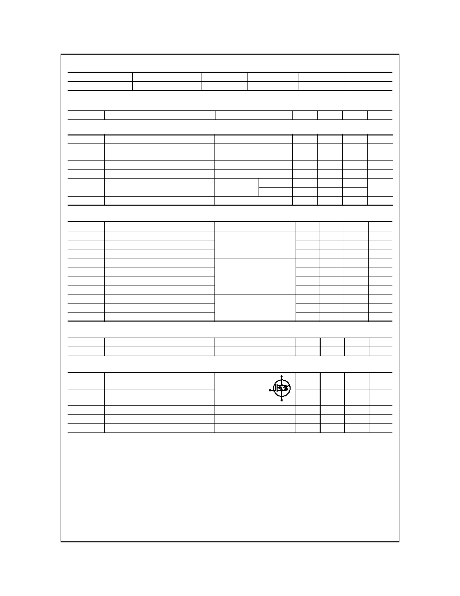
Absolute Maximum Ratings
T
C
= 25
o
C unless otherwise noted
Thermal Characteristics
Symbol
Parameter
Ratings
Units
V
DSS
Drain to Source Voltage
500
V
V
GS
Gate to Source Voltage
±
30
V
I
D
Drain Current
Continuous (T
C
= 25
o
C, V
GS
= 10V)
44
A
Continuous (T
C
= 100
o
C, V
GS
= 10V)
32
A
Pulsed
1
176
A
P
D
Power dissipation
750
W
Derate above 25
o
C
5
W/
o
C
T
J
, T
STG
Operating and Storage Temperature
-55 to 175
o
C
Soldering Temperature for 10 seconds
300 (1.6mm from case)
o
C
Mounting Torque, 8-32 or M3 Screw
10ibf*in (1.1N*m)
R
JC
Thermal Resistance Junction to Case
0.2
o
C/W
R
CS
Thermal Resistance Case to Sink, Flat, Greased Surface
0.24
o
C/W
R
JA
Thermal Resistance Junction to Ambient
40
o
C/W
©2002 Fairchild Semiconductor Corporation
FDH44N50 Rev. A4, August 2002
FDH44N50
Package Marking and Ordering Information
Electrical Characteristics
T
J
= 25∞C (unless otherwise noted)
Statics
Dynamics
Avalanche Characteristics
Drain-Source Diode Characteristics
Notes:
1: Repetitive rating; pulse width limited by maximum junction temperature
2: Starting T
J
= 25∞C, L = 1.61mH, I
AS
= 44
Device Marking
Device
Package
Reel Size
Tape Width
Quantity
FDH44N50
FDH44N50
TO-247
-
-
30
Symbol
Parameter
Test Conditions
Min
Typ
Max
Units
B
VDSS
Drain to Source Breakdown Voltage
I
D
= 250
µ
A, V
GS
= 0V
500
-
-
V
B
VDSS
/
T
J
Breakdown Voltage Temp. Coefficient
Reference to 25
o
C,
ID = 1mA
-
0.61
-
V/∞C
r
DS(ON)
Drain to Source On-Resistance
V
GS
= 10V, I
D
= 22A
-
0.11
0.12
V
GS(th)
Gate Threshold Voltage
V
DS
= V
GS
, I
D
= 250
µA
2
3.15
4
V
I
DSS
Zero Gate Voltage Drain Current
V
DS
= 500V
T
C
= 25
o
C
-
-
25
µ
A
V
GS
= 0V
T
C
= 150
o
C
-
-
250
I
GSS
Gate to Source Leakage Current
V
GS
= ±20V
-
-
±100
nA
g
fs
Forward Transconductance
V
DS
= 50V, I
D
= 22A
11
-
-
S
Q
g(TOT)
Total Gate Charge at 10V
V
GS
= 10V,
V
DS
= 400V,
I
D
= 44A
-
90
108
nC
Q
gs
Gate to Source Gate Charge
-
24
29
nC
Q
gd
Gate to Drain "Miller" Charge
-
31
37
nC
t
d(ON)
Turn-On Delay Time
V
DD
= 250V,
I
D
= 44A,
R
G
= 2.15
,
R
D
= 5.68
-
16
-
ns
t
r
Rise Time
-
84
-
ns
t
d(OFF)
Turn-Off Delay Time
-
45
-
ns
t
f
Fall Time
-
79
-
ns
C
ISS
Input Capacitance
V
DS
= 25V, V
GS
= 0V,
f = 1MHz
-
5335
-
pF
C
OSS
Output Capacitance
-
645
-
pF
C
RSS
Reverse Transfer Capacitance
-
40
-
pF
E
AS
Single Pulse Avalanche Energy
2
1500
-
-
mJ
I
AR
Avalanche Current
-
-
44
A
I
S
Continuous Source Current
(Body Diode)
MOSFET symbol
showing the
integral reverse
p-n junction diode.
-
-
44
A
I
SM
Pulsed Source Current
1
(Body Diode)
-
-
176
A
V
SD
Source to Drain Diode Voltage
I
SD
= 44A
-
0.900
1.2
V
t
rr
Reverse Recovery Time
I
SD
= 44A, dI
SD
/dt = 100A/
µ
s
-
920
1100
ns
Q
RR
Reverse Recovered Charge
I
SD
= 44A, dI
SD
/dt = 100A/
µ
s
-
14
18
µ
C
D
G
S
©2002 Fairchild Semiconductor Corporation
FDH44N50 Rev. A4, August 2002
FDH44N50
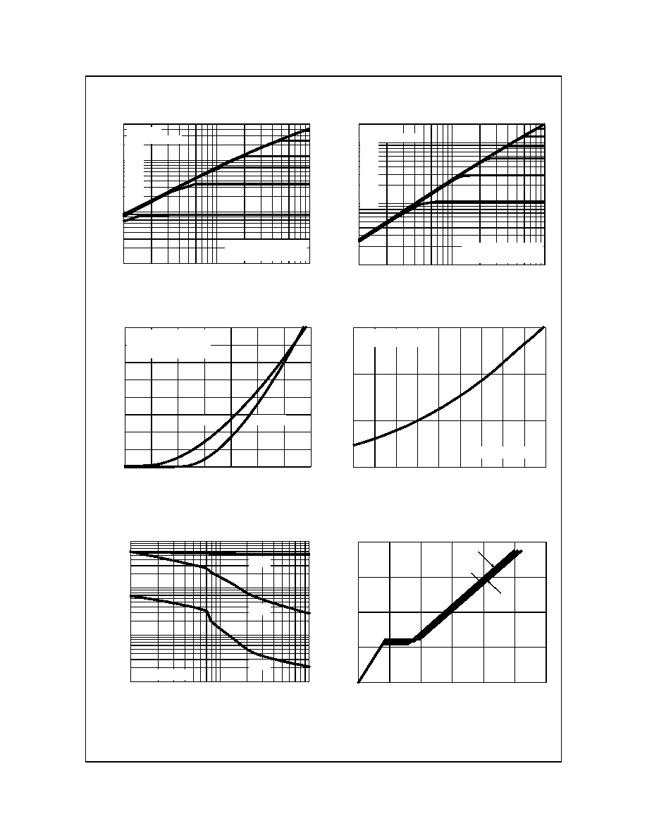
Typical Characteristic
Figure 1. Output Characteristics
Figure 2. Output Characteristics
Figure 3. Transfer Characteristics
Figure 4. Normalized Drain To Source On
Resistance vs Junction Temperatrue
Figure 5. Capacitance vs Drain To Source Voltage
Figure 6. Gate Charge Waveforms For Constant
Gate Current
1
10
100
500
1
10
100
VDS, DRAIN TO SOURCE VOLTAGE (V)
ID, DRAIN
T
O
SOU
RCE
CURRENT
(
A
)
PULSE DURATION = 80
µ
s
DUTY CYCLE = 0.5% MAX
VGS DESCENDING
TJ = 25
o
C
6V
5.5V
4.5V
5V
8V
10V
1
10
100
200
1
10
100
VDS, DRAIN TO SOURCE VOLTAGE (V)
ID, DRAIN
T
O
SOURCE CURRENT
(
A
)
PULSE DURATION = 80
µ
s
DUTY CYCLE = 0.5% MAX
VGS DESCENDING
TJ = 175
o
C
5.5V
5V
4V
4.5V
6V
6.5V
10V
0
20
40
60
80
100
120
140
160
3.0
3.5
4.0
4.5
5.0
5.5
6.0
6.5
ID
, DR
AIN CURRENT
(
A
)
VGS, GATE TO SOURCE VOLTAGE (V)
TJ = 175
o
C
TJ = 25
o
C
PULSE DURATION = 80
µ
s
DUTY CYCLE = 0.5% MAX
VDD = 80V
0
1
2
3
-50
-25
0
25
50
75
100
125
150
175
NORM
AL
IZ
ED DRAIN t
o
S
O
U
RCE ON RES
I
S
T
ANC
E
TJ, JUNCTION TEMPERATURE (
o
C)
PULSE DURATION = 80
µ
s
DUTY CYCLE = 0.5% MAX
VGS = 10V, ID = 22A
C, CAPACIT
ANCE (
p
F
)
VDS, DRAIN TO SOURCE VOLTAGE (V)
VGS = 0V, f = 1MHz
10
100
1000
10000
1
10
100
CRSS
COSS
CISS
VG
S
,
GAT
E
t
o
SOURCE VOL
T
A
G
E (
V
)
Qg, GATE CHARGE (nC)
ID = 44A
400V
100V
0
4
8
12
16
0
25
50
75
100
125
150
250V
©2002 Fairchild Semiconductor Corporation
FDH44N50 Rev. A4, August 2002
FDH44N50
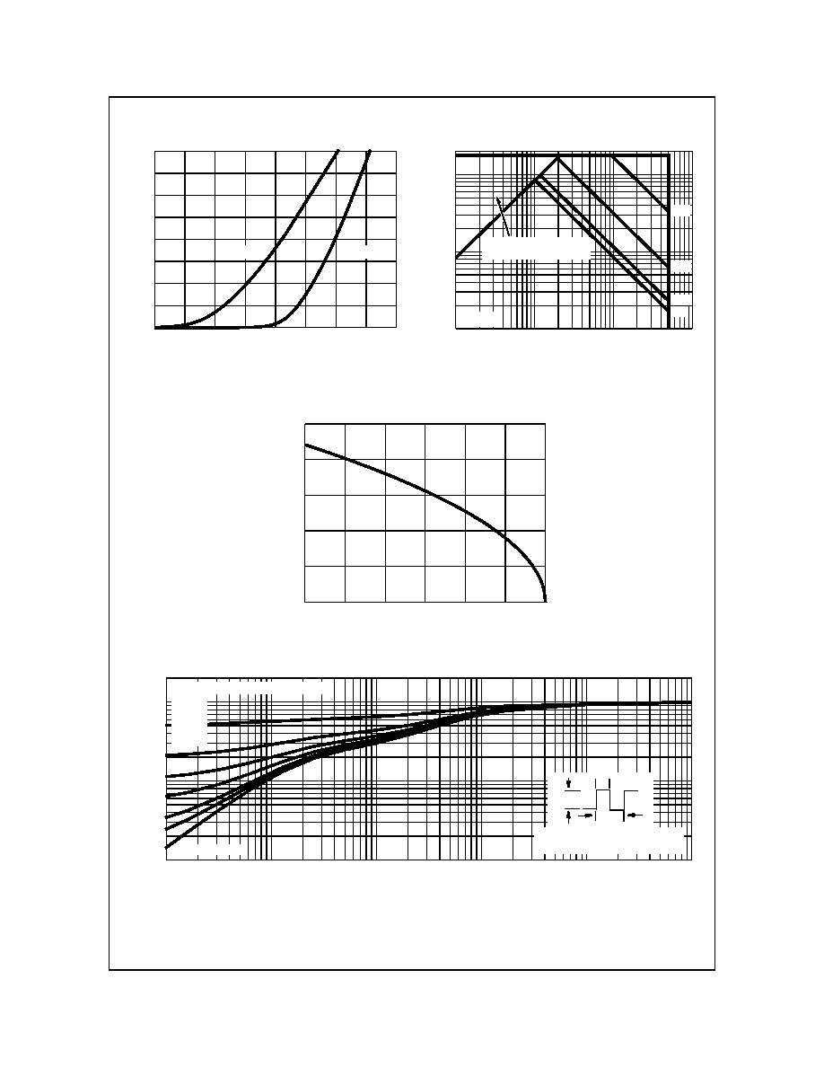
Figure 7. Body Diode Forward Voltage vs Body
Diode Current
Figure 8. Maximum Safe Operating Area
Figure 9. Maximum Drain Current vs Case Temperature
Figure 10. Normalized Transient Thermal Impedance, Junction to Case
Typical Characteristic
(Continued)
0
10
20
30
40
50
60
70
80
0.3
0.4
0.5
0.6
0.7
0.8
0.9
1.0
1.1
I
SD
, SOURCE T
O
DR
AIN CURRENT
(
A
)
V
SD
, SOURCE TO DRAIN VOLTAGE (V)
T
J
= 25
o
C
T
J
= 175
o
C
1
10
100
200
1
10
100
1000
ID, D
RAIN CURRENT
(
A
)
VDS, DRAIN TO SOURCE VOLTAGE (V)
OPERATION IN THIS AREA
LIMITED BY RDS(ON)
1ms
100µs
DC
TC = 25
o
C
10ms
TC, CASE TEMPERATURE (∞C)
I
D
, DRAIN
CURRENT
(
A
)
0
10
20
30
40
50
25
50
75
100
125
150
175
t1, RECTANGULAR PULSE DURATION (S)
Z
J
C
,
N
O
R
M
A
L
I
Z
E
D T
H
ERM
A
L
RE
SPONSE
1
10
-3
10
-2
10
-1
10
0
10
-
4
t1
t2
PD
DUTY FACTOR, D = t1 / t2
PEAK TJ = (PD X Z
JC X R
JC) + TC
SINGLE PULSE
0.1
0.01
10
-5
0.5
0.2
0.1
0.05
0.02
0.01
DUTY CYCLE DESENDING ORDER
©2002 Fairchild Semiconductor Corporation
FDH44N50 Rev. A4, August 2002
FDH44N50
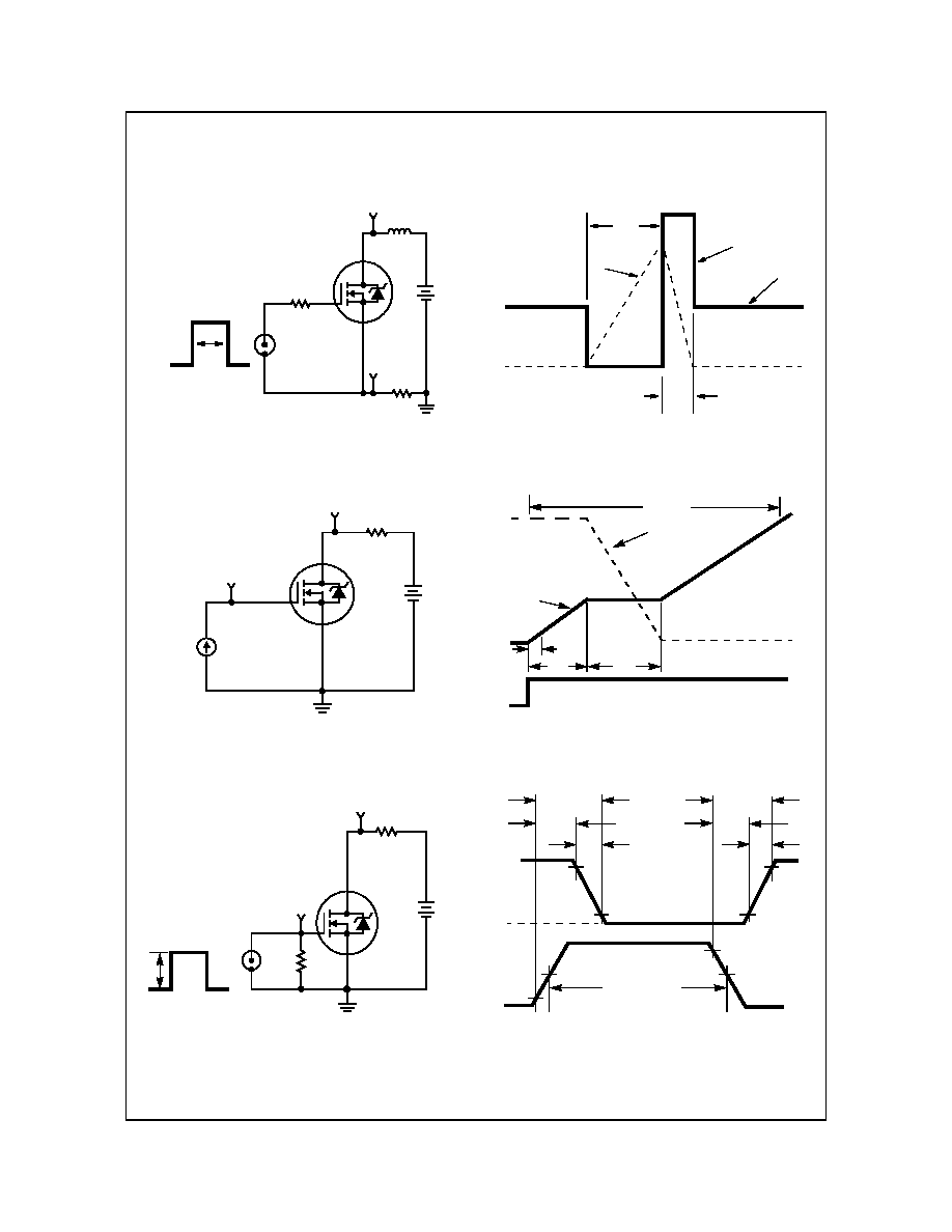
Test Circuits and Waveforms
Figure 11. Unclamped Energy Test Circuit
Figure 12. Unclamped Energy Waveforms
Figure 13. Gate Charge Test Circuit
Figure 14. Gate Charge Waveforms
Figure 15. Switching Time Test Circuit
Figure 16. Switching Time Waveform
t
P
V
GS
0.01
L
I
AS
+
-
V
DS
V
DD
R
G
DUT
VARY t
P
TO OBTAIN
REQUIRED PEAK I
AS
0V
V
DD
V
DS
BV
DSS
t
P
I
AS
t
AV
0
R
L
V
GS
+
-
V
DS
V
DD
DUT
I
g(REF)
V
DD
Q
g(TH)
V
GS
= 1V
Q
g(TOT)
V
GS
= 10V
V
DS
V
GS
I
g(REF)
0
0
Q
gs
Q
gd
V
GS
R
L
R
GS
DUT
+
-
V
DD
V
DS
V
GS
t
ON
t
d(ON)
t
r
90%
10%
V
DS
90%
10%
t
f
t
d(OFF)
t
OFF
90%
50%
50%
10%
PULSE WIDTH
V
GS
0
0

DISCLAIMER
FAIRCHILD SEMICONDUCTOR RESERVES THE RIGHT TO MAKE CHANGES WITHOUT FURTHER
NOTICE TO ANY PRODUCTS HEREIN TO IMPROVE RELIABILITY, FUNCTION OR DESIGN. FAIRCHILD
DOES NOT ASSUME ANY LIABILITY ARISING OUT OF THE APPLICATION OR USE OF ANY PRODUCT
OR CIRCUIT DESCRIBED HEREIN; NEITHER DOES IT CONVEY ANY LICENSE UNDER ITS PATENT
RIGHTS, NOR THE RIGHTS OF OTHERS.
TRADEMARKS
The following are registered and unregistered trademarks Fairchild Semiconductor owns or is authorized to use and is
not intended to be an exhaustive list of all such trademarks.
LIFE SUPPORT POLICY
FAIRCHILDS PRODUCTS ARE NOT AUTHORIZED FOR USE AS CRITICAL COMPONENTS IN LIFE SUPPORT
DEVICES OR SYSTEMS WITHOUT THE EXPRESS WRITTEN APPROVAL OF FAIRCHILD SEMICONDUCTOR CORPORATION.
As used herein:
1. Life support devices or systems are devices or
systems which, (a) are intended for surgical implant into
the body, or (b) support or sustain life, or (c) whose
failure to perform when properly used in accordance
with instructions for use provided in the labeling, can be
reasonably expected to result in significant injury to the
user.
2. A critical component is any component of a life
support device or system whose failure to perform can
be reasonably expected to cause the failure of the life
support device or system, or to affect its safety or
effectiveness.
PRODUCT STATUS DEFINITIONS
Definition of Terms
Datasheet Identification
Product Status
Definition
Advance Information
Preliminary
No Identification Needed
Obsolete
This datasheet contains the design specifications for
product development. Specifications may change in
any manner without notice.
This datasheet contains preliminary data, and
supplementary data will be published at a later date.
Fairchild Semiconductor reserves the right to make
changes at any time without notice in order to improve
design.
This datasheet contains final specifications. Fairchild
Semiconductor reserves the right to make changes at
any time without notice in order to improve design.
This datasheet contains specifications on a product
that has been discontinued by Fairchild semiconductor.
The datasheet is printed for reference information only.
Formative or
In Design
First Production
Full Production
Not In Production
ImpliedDisconnect
ISOPLANAR
LittleFET
MicroFET
MicroPak
MICROWIRE
MSX
MSXPro
OCX
OCXPro
OPTOLOGIC
‚
OPTOPLANAR
FACT
FACT Quiet Series
FAST
‚
FASTr
FRFET
GlobalOptoisolator
GTO
HiSeC
I
2
C
Rev. I1
ACEx
ActiveArray
Bottomless
CoolFET
CROSSVOLT
DOME
EcoSPARK
E
2
CMOS
TM
EnSigna
TM
PACMAN
POP
Power247
PowerTrench
‚
QFET
QS
QT Optoelectronics
Quiet Series
RapidConfigure
RapidConnect
SILENT SWITCHER
‚
SMART START
SPM
Stealth
SuperSOT-3
SuperSOT-6
SuperSOT-8
SyncFET
TinyLogic
TruTranslation
UHC
UltraFET
‚
VCX
Across the board. Around the world.
The Power Franchise
Programmable Active Droop