 | –≠–ª–µ–∫—Ç—Ä–æ–Ω–Ω—ã–π –∫–æ–º–ø–æ–Ω–µ–Ω—Ç: FDH50N50 | –°–∫–∞—á–∞—Ç—å:  PDF PDF  ZIP ZIP |
©2004 Fairchild Semiconductor Corporation
1
www.fairchildsemi.com
FDH50N50 / FDA50N50 Rev. A
FD
H5
0N
5
0
/
FDA
5
0N
50
5
00V
N
-
Cha
nnel M
O
S
F
ET
UniFET
TM
FDH50N50 / FDA50N50
500V N-Channel MOSFET
Features
∑ 48A, 500V, R
DS(on)
= 0.105
@V
GS
= 10 V
∑ Low gate charge ( typical 105 nC)
∑ Low C
rss
( typical 45 pF)
∑ Fast switching
∑ 100% avalanche tested
∑ Improved dv/dt capability
Description
These N-Channel enhancement mode power field effect transis-
tors are produced using Fairchild's proprietary, planar stripe,
DMOS technology.
This advanced technology has been especially tailored to mini-
mize on-state resistance, provide superior switching perfor-
mance, and withstand high energy pulse in the avalanche and
commutation mode. These devices are well suited for high effi-
cient switched mode power supplies and active power factor
correction.
Absolute Maximum Ratings
Thermal Characteristics
! "
!
!
!
"
"
"
! "
!
!
!
"
"
"
S
D
G
G
S
D
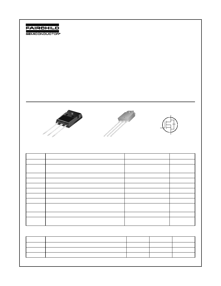
TO-247
FDH Series
G
S
D
TO-3P
FDA Series
Symbol
Parameter
FDH50N50/FDA50N50
Unit
V
DSS
Drain-Source Voltage
500
V
I
D
Drain Current
- Continuous (T
C
= 25
∞
C)
- Continuous (T
C
= 100
∞
C)
48
30.8
A
A
I
DM
Drain Current
- Pulsed
(Note 1)
192
A
V
GSS
Gate-Source voltage
±
20
V
E
AS
Single Pulsed Avalanche Energy
(Note 2)
1868
mJ
I
AR
Avalanche Current
(Note 1)
48
A
E
AR
Repetitive Avalanche Energy
(Note 1)
62.5
mJ
dv/dt
Peak Diode Recovery dv/dt
(Note 3)
4.5
V/ns
P
D
Power Dissipation
(T
C
= 25
∞
C)
- Derate above 25
∞
C
625
5
W
W/
∞
C
T
J,
T
STG
Operating and Storage Temperature Range
-55 to +150
∞
C
T
L
Maximum Lead Temperature for Soldering Purpose,
1/8" from Case for 5 Seconds
300
∞
C
Symbol
Parameter
Min.
Max.
Unit
R
JC
Thermal Resistance, Junction-to-Case
--
0.2
∞
C/W
R
CS
Thermal Resistance, Case-to-Sink
0.24
--
∞
C/W
R
JA
Thermal Resistance, Junction-to-Ambient
--
40
∞
C/W

2
www.fairchildsemi.com
FDH50N50 / FDA50N50 Rev. A
FD
H5
0N
5
0
/
FDA
5
0N
50
5
00V
N
-
Cha
nnel M
O
S
F
ET
Package Marking and Ordering Information
Electrical Characteristics
T
C
= 25∞C unless otherwise noted
NOTES:
1. Repetitive Rating: Pulse width limited by maximum junction temperature
2. L = 1.46mH, I
AS
= 48A, V
DD
= 50V, R
G
= 25
, Starting T
J
= 25
∞
C
3. I
SD
48A, di/dt
200A/
µ
s, V
DD
BV
DSS
, Starting T
J
= 25
∞
C
4. Pulse Test: Pulse width
300
µ
s, Duty Cycle
2%
5. Essentially Independent of Operating Temperature Typical Characteristics
Device Marking
Device
Package
Reel Size
Tape Width
Quantity
FDH50N50
FDH50N50
TO-247
-
-
30
FDA50N50
FDA50N50
TO-3P
-
-
30
Symbol
Parameter
Conditions
Min.
Typ.
Max Units
Off Characteristics
BV
DSS
Drain-Source Breakdown Voltage
V
GS
= 0V, I
D
= 250
µ
A
500
--
--
V
BV
DSS
/
T
J
Breakdown Voltage Temperature
Coefficient
I
D
= 250
µ
A, Referenced to 25
∞
C
--
0.5
--
V/
∞
C
I
DSS
Zero Gate Voltage Drain Current
V
DS
= 500V, V
GS
= 0V
V
DS
= 400V, T
C
= 125
∞
C
--
--
--
--
25
250
µ
A
µ
A
I
GSSF
Gate-Body Leakage Current, Forward
V
GS
= 20V, V
DS
= 0V
--
--
100
nA
I
GSSR
Gate-Body Leakage Current, Reverse
V
GS
= -20V, V
DS
= 0V
--
--
-100
nA
On Characteristics
V
GS(th)
Gate Threshold Voltage
V
DS
= V
GS
, I
D
= 250
µ
A
3.0
--
5.0
V
R
DS(on)
Static Drain-Source
On-Resistance
V
GS
= 10V, I
D
= 24A
--
0.089
0.105
g
FS
Forward Transconductance
V
DS
= 40V, I
D
= 48A
(Note 4)
--
20
--
S
Dynamic Characteristics
C
iss
Input Capacitance
V
DS
= 25V, V
GS
= 0V,
f = 1.0MHz
--
4979
6460
pF
C
oss
Output Capacitance
--
760
1000
pF
C
rss
Reverse Transfer Capacitance
--
50
65
pF
C
oss
Output Capacitance
V
DS
= 400V, V
GS
= 0V, f = 1.0MHz
--
161
--
pF
C
oss
eff.
Effective Output Capacitance
V
DS
= 0V to 400V, V
GS
= 0V
--
342
--
pF
Switching Characteristics
t
d(on)
Turn-On Delay Time
V
DD
= 250V, I
D
= 48A
R
G
= 25
(Note 4, 5)
--
105
220
ns
t
r
Turn-On Rise Time
--
360
730
ns
t
d(off)
Turn-Off Delay Time
--
225
460
ns
t
f
Turn-Off Fall Time
--
230
470
ns
Q
g
Total Gate Charge
V
DS
= 400V, I
D
= 48A
V
GS
= 10V
(Note 4, 5)
--
105
137
nC
Q
gs
Gate-Source Charge
--
33
--
nC
Q
gd
Gate-Drain Charge
--
45
--
nC
Drain-Source Diode Characteristics and Maximum Ratings
I
S
Maximum Continuous Drain-Source Diode Forward Current
--
--
48
A
I
SM
Maximum Pulsed Drain-Source Diode Forward Current
--
--
192
A
V
SD
Drain-Source Diode Forward Voltage
V
GS
= 0V, I
S
= 48A
--
--
1.4
V
t
rr
Reverse Recovery Time
V
GS
= 0V, I
S
= 48A
dI
F
/dt =100A/
µ
s
(Note 4)
--
580
--
ns
Q
rr
Reverse Recovery Charge
--
10
--
µ
C

3
www.fairchildsemi.com
FDH50N50 / FDA50N50 Rev. A
FD
H5
0N
5
0
/
FDA
5
0N
50
5
00V
N
-
Cha
nnel M
O
S
F
ET
Typical Performance Characteristics
Figure 1. On-Region Characteristics
Figure 2. Transfer Characteristics
Figure 3. On-Resistance Variation vs.
Figure 4. Body Diode Forward Voltage
Drain Current and Gate Voltage
Variation vs. Source Current
and Temperatue
Figure 5. Capacitance Characteristics
Figure 6. Gate Charge Characteristics
10
-1
10
0
10
1
10
-1
10
0
10
1
10
2
V
GS
Top : 15.0 V
10.0 V
8.0 V
7.0 V
6.5 V
6.0 V
Bottom : 5.5 V
Notes :
1. 250
µ
s Pulse Test
2. T
C
= 25
o
C
!
I
D
,
Dr
a
i
n
C
u
r
r
ent
[
A
]
V
DS
, Drain-Source Voltage [V]
4
5
6
7
8
9
10
0.1
1
10
100
Notes :
1. V
DS
= 40V
2. 250
µ
s Pulse Test
-55
o
C
!
150
o
C
!
25
o
C
!
I
D
, Drain
Cu
r
r
e
n
t [A]
V
GS
, Gate-Source Voltage [V]
0
25
50
75
100
125
150
175
0.0
0.1
0.2
0.3
0.4
V
GS
= 20V
V
GS
= 10V
Note : T
J
= 25
o
C
R
DS
(
O
N)
[
],
D
r
ai
n-
S
o
u
r
ce O
n
-
R
es
is
t
ance
I
D
, Drain Current [A]
0.2
0.4
0.6
0.8
1.0
1.2
1.4
1.6
0
40
80
120
160
25
o
C
150
o
C
Notes :
1. V
GS
= 0V
2. 250
µ
s Pulse Test
I
DR
,
R
e
ver
s
e D
r
ain C
u
rr
en
t
[
A
]
V
SD
, Source-Drain Voltage [V]
10
-1
10
0
10
1
10
2
0
2,000
4,000
6,000
8,000
10,000
12,000
C
iss
= C
gs
+ C
gd
(C
ds
= shorted)
C
oss
= C
ds
+ C
gd
C
rss
= C
gd
Notes :
1. V
GS
= 0 V
2. f = 1 MHz
C
rss
C
oss
C
iss
C
apa
c
i
t
a
nc
e [p
F]
V
DS
, Drain-Source Voltage [V]
0
20
40
60
80
100
120
0
2
4
6
8
10
12
V
DS
= 250V
V
DS
= 100V
V
DS
= 400V
Note : I
D
= 48A
V
GS
, G
a
te-
S
ource
V
o
ltage
[V
]
Q
G
, Total Gate Charge [nC]

4
www.fairchildsemi.com
FDH50N50 / FDA50N50 Rev. A
FD
H5
0N
5
0
/
FDA
5
0N
50
5
00V
N
-
Cha
nnel M
O
S
F
ET
Typical Performance Characteristics
(Continued)
Figure 7. Breakdown Voltage Variation
Figure 8. On-Resistance Variation
vs. Temperature
vs. Temperature
Figure 9. Maximum Safe Operating Area
Figure 10. Maximum Drain Current
vs. Case Temperature
Figure 11. Typical Drain Current Slope
Figure 12. Typical Drain-Source Voltage
vs. Gate Resistance
Slope vs. Gate Resistance
-100
-50
0
50
100
150
200
0.8
0.9
1.0
1.1
1.2
Notes :
1. V
GS
= 0 V
2. I
D
= 250
µ
A
BV
DSS
,
(
N
o
r
m
a
lize
d
)
D
r
ai
n-
So
ur
c
e
B
r
eak
do
w
n
V
o
l
t
age
T
J
, Junction Temperature [
o
C]
-100
-50
0
50
100
150
200
0.0
0.5
1.0
1.5
2.0
2.5
Notes :
1. V
GS
= 10 V
2. I
D
= 24 A
R
DS(
O
N)
, (N
or
malized)
D
r
ain-S
our
c
e
On-R
esistance
T
J
, Junction Temperature [
o
C]
10
0
10
1
10
2
10
3
10
-1
10
0
10
1
10
2
10
3
10 us
DC
10 ms
1 ms
100 us
Operation in This Area
is Limited by R
DS(on)
Notes :
1. T
C
= 25
o
C
2. T
J
= 150
o
C
3. Single Pulse
I
D
, D
r
a
i
n Curren
t
[A
]
V
DS
, Drain-Source Voltage [V]
25
50
75
100
125
150
0
10
20
30
40
50
I
D
,
D
r
ai
n C
u
r
r
e
n
t
[
A
]
T
C
, Case Temperature [
o
C]
0
5
10
15
20
25
30
35
40
45
50
0
5
10
15
20
25
30
35
40
45
Notes :
1. V
DS
= 400 V
2. V
GS
= 12 V
3. I
D
= 25A
4. T
J
= 125
o
C
!
dv/dt(off)
dv/dt(on)
dv
/d
t [V
/n
S]
R
G
, Gate resistance [
]
0
5
10
15
20
25
30
35
40
45
50
0
500
1,000
1,500
2,000
2,500
3,000
3,500
4,000
Notes :
1. V
DS
= 400 V
2. V
GS
= 12 V
3. I
D
= 25A
4. T
J
= 125
o
C
di/dt(off)
di/dt(on)
d
i
/dt [A/
µ
S]
R
G
, Gate resistance [
]

5
www.fairchildsemi.com
FDH50N50 / FDA50N50 Rev. A
FD
H5
0N
5
0
/
FDA
5
0N
50
5
00V
N
-
Cha
nnel M
O
S
F
ET
Typical Performance Characteristics
(Continued)
Figure 13. Typical Switching Losses vs.
Figure 14. Unclamped Inductive Switching
Gate Resistance
Capability
Figure 15. Transient Thermal Resistance Curve
0
5
10
15
20
25
30
35
40
45
50
0
200
400
600
800
1,000
Notes :
1. V
DS
= 400 V
2. V
GS
= 12 V
3. I
D
= 25A
4. T
J
= 125
o
C
!
Eoff
Eon
E
nergy
[
µ
J]
R
G
, Gate resistance [
]
0.01
0.1
1
10
100
1
10
100
Starting T
J
= 150
o
C
Notes :
1. If R = 0
t
AV
= (L)(I
AS
)/(1.3 Rated BV
DSS
- V
DD
)
2. If R
0
t
AV
= (L/R)In[(I
AS
x R)/(1.3 Rated BV
DSS
- V
DD
)+1]
Starting T
J
= 25
o
C
I
AS
,
A
v
al
anc
he C
u
rrent
[
A
]
t
AV
, Time In Avalanche [ms]
10
-5
10
-4
10
-3
10
-2
10
-1
10
0
10
1
10
-3
10
-2
10
-1
Notes :
1. Z
JC
(t) = 0.2
o
C/W Max.
2. Duty Factor, D=t
1
/t
2
3. T
JM
- T
C
= P
DM
* Z
JC
(t)
single pulse
D=0.5
0.02
0.2
0.05
0.1
0.01
Z
JC
(
t
)
,
T
her
mal
Re
spo
n
se
t
1
, Square W ave Pulse Duration [sec]