 | –≠–ª–µ–∫—Ç—Ä–æ–Ω–Ω—ã–π –∫–æ–º–ø–æ–Ω–µ–Ω—Ç: FDMS8690 | –°–∫–∞—á–∞—Ç—å:  PDF PDF  ZIP ZIP |

March 2006
©
2006 Fairchild Semiconductor Corporation
FDMS8690 Rev B(W)
www.fairchildsemi.com
FDMS8690
N-Channel PowerTrench
Æ
MOSFET
30V, 19.8A, 9m
General Description
This device has been designed specifically to improve
the efficiency of DC-DC converters. Using new
techniques in MOSFET construction, the various
components of gate charge and capacitance have been
optimized to reduce switching losses. Low gate
resistance and very low Miller charge enable excellent
performance with both adaptive and fixed dead time
gate drive circuits. Very low r
DS(on)
has been maintained
to provide an extremely versatile device.
Applications
High Efficiency DC-DC Converters
Notebook Vcore Power Supply
Multi purpose Point of Load
Features
Max
r
DS(on)
= 9.0m
at V
GS
= 10V, I
D
= 19.8A
Max
r
DS(on)
= 12.5m
at V
GS
= 4.5V, I
D
= 11.5A
High performance trench technology for extremely
low r
DS(on)
and gate charge
Minimal Qgd (2.9 nC typical)
RoHS
Compliant
Absolute Maximum Ratings
T
A
=25
o
C unless otherwise noted
Symbol Parameter
Ratings
Units
V
DS
Drain-Source Voltage
30
V
V
GS
Gate-Source
Voltage
±
20
V
I
D
Drain Current ≠ Continuous
(Note 1a)
19.8 A
≠
Pulsed
90
Power Dissipation for Single Operation
(Note 1a)
2.8
P
D
(Note 1b)
1.1
W
T
J
, T
STG
Operating and Storage Junction Temperature Range
≠55 to +150
∞
C
Thermal Characteristics
R
JA
Thermal Resistance, Junction-to-Ambient
(Note 1a)
44
∞
C/W
R
JA
Thermal Resistance, Junction-to-Ambient
(Note 1b)
115
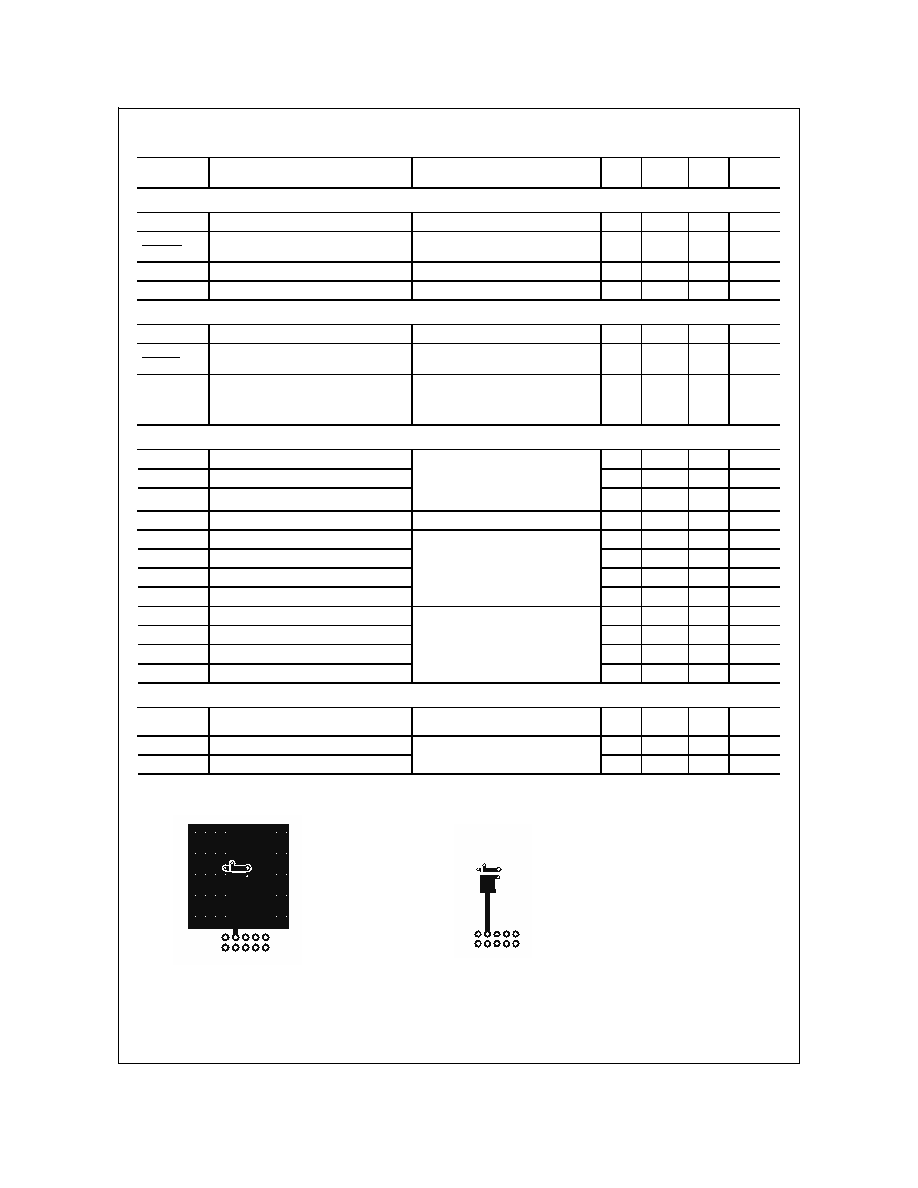
Package Marking and Ordering Information
Device Marking
Device
Reel Size
Tape width
Quantity
FDMS8690
FDMS8690
7''
12mm
3000 units
4
3
2
1
5
6
7
8
FDM
S86
9
0
N-
C
h
a
nn
e
l P
o
w
e
rTr
e
n
c
h
Æ
M
OS
FET
S S S G
D D D D
PIN 1
MLP 5X6
D
FDMS8690 Rev B(W)
www.fairchildsemi.com
Electrical Characteristics
T
A
= 25∞C unless otherwise noted
Symbol Parameter
Test
Conditions
Min
Typ
Max
Units
Off Characteristics
BV
DSS
Drain≠Source Breakdown Voltage
V
GS
= 0 V,
I
D
= 250
µ
A
30 V
BV
DSS
T
J
Breakdown Voltage Temperature
Coefficient
I
D
= 250
µ
A, Referenced to 25
∞
C
34
mV/
∞
C
I
DSS
Zero Gate Voltage Drain Current
V
DS
= 24 V,
V
GS
= 0 V
1
µ
A
I
GSS
Gate≠Body
Leakage
V
GS
=
±
20 V, V
DS
= 0 V
±
100
nA
On Characteristics
(Note 2)
V
GS(th)
Gate Threshold Voltage
V
DS
= V
GS
,
I
D
= 250
µ
A
1 1.6 3 V
V
GS(th)
T
J
Gate Threshold Voltage
Temperature Coefficient
I
D
= 250
µ
A, Referenced to 25
∞
C
≠4.5 mV/
∞
C
r
DS(on)
Static Drain≠Source
On≠Resistance
V
GS
= 10 V,
I
D
= 19.8 A
V
GS
= 4.5 V, I
D
= 11.5 A
V
GS
= 10 V, I
D
=19.8A, T
J
= 125
∞
C
7.4
9.9
10.6
9
12.5
13.3
m
Dynamic Characteristics
C
iss
Input
Capacitance
1260
1680
pF
C
oss
Output
Capacitance
535
715
pF
C
rss
Reverse Transfer Capacitance
V
DS
= 15 V,
V
GS
= 0 V,
f = 1.0 MHz
80
120
pF
R
G
Gate Resistance
f = 1.0 MHz
1.1
t
d(on)
Turn≠On
Delay
Time
8
16
ns
t
r
Turn≠On Rise Time
1.8
10
ns
t
d(off)
Turn≠Off Delay Time
26
42
ns
t
f
Turn≠Off
Fall
Time
V
DD
= 15 V,
I
D
= 1 A,
V
GS
= 10 V,
R
GEN
= 6
19
35 ns
Q
g(TOT)
Total Gate Charge at V
GS
= 10V
18.8
27
nC
Q
g(5)
Total Gate Charge at V
GS
= 5V
10
14
nC
Q
gs
Gate≠Source
Charge
3.5
nC
Q
gd
Gate≠Drain
Charge
V
DS
= 15 V,
I
D
= 14 A
2.9 nC
Drain≠Source Diode Characteristics
V
SD
Drain≠Source Diode Forward
Voltage
V
GS
= 0 V, I
S
= 2.1 A
(Note 2)
0.7 1.2 V
t
rr
Diode Reverse Recovery Time
45
ns
Q
rr
Diode Reverse Recovery Charge
I
F
= 14 A,
di/dt = 100 A/µs
33
nC
Notes:
1.
R
JA
is determined with the device mounted on a 1in
2
pad 2 oz copper pad on a 1.5 x 1.5 in. board of FR-4 material. R
JC
is guaranteed by design
while R
CA
is determined by the user's board design.
a) 44∞C/W
when
mounted on a 1in
2
pad
of 2 oz copper
b)
115 ∞C/W when mounted
on a minimum pad of 2 oz
copper
Scale 1 : 1 on letter size paper
2. Pulse Test: Pulse Width < 300
µ
s, Duty Cycle < 2.0%
FDM
S86
9
0
N-
C
h
a
nn
e
l P
o
w
e
rTr
e
n
c
h
Æ
M
OS
FET

FD
M
S86
90 N-
Channel
Powe
rTr
enc
h
Æ
MO
SFET
FD
MS8690 Rev. B
www.fairchildsemi.com
3
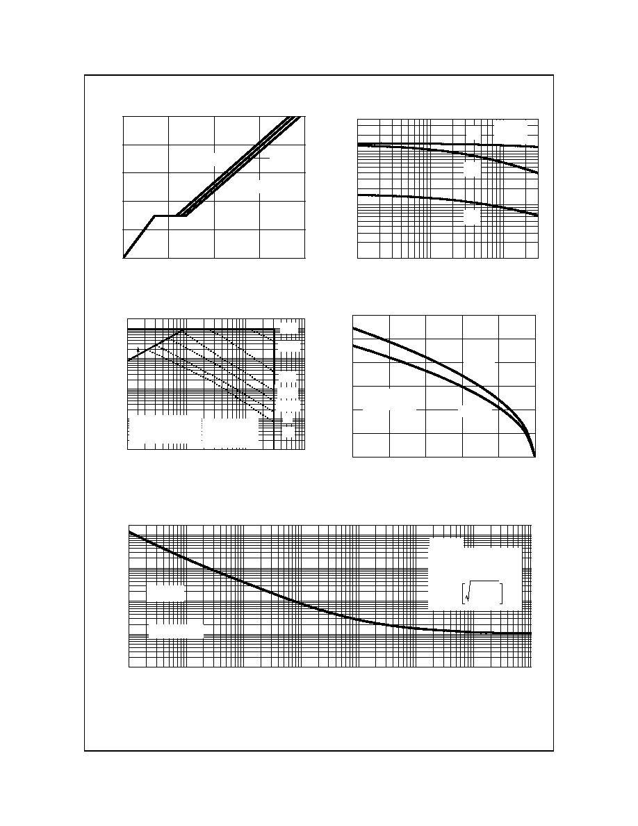
Typical Characteristics
T
J
= 25∞C unless otherwise noted
Figure 1.
0
1
2
3
4
0
20
40
60
80
100
I
D
, DR
AIN CU
R
REN
T (A)
V
DS
, DRAIN TO SOURCE VOLTAGE (V)
V
GS
= 4V
V
GS
= 4.5V
V
GS
= 3.5V
V
GS
=
10V
V
GS
= 3V
V
GS
= 4.5V
PULSE DURATION = 80
µ
s
DUTY CYCLE = 0.5%MAX
On Region Characteristics
Figure 2.
0
20
40
60
80
100
0.8
1.2
1.6
2.0
2.4
2.8
3.2
I
D
, DRAIN CURRENT(A)
PULSE DURATION = 80
µ
s
DUTY CYCLE = 0.5%MAX
V
GS
=
4V
V
GS
=
3.5V
V
GS
= 3.0V
V
GS
=
10V
V
GS
=
4.5V
NO
R
M
AL
IZ
E
D
DR
AI
N
TO
S
O
URC
E
O
N
-
R
E
S
I
S
T
A
NC
E
Normal On-Resistance vs Drain Current
and Gate Voltage
Figure 3. Normalized
-80
-40
0
40
80
120
160
0.6
0.8
1.0
1.2
1.4
1.6
I
D
= 14A
V
GS
= 10V
NO
RM
AL
I
Z
E
D
DR
AIN T
O
SO
U
R
C
E
O
N
-R
ESIST
A
N
C
E
T
J
, JUNCTION TEMPERATURE (
o
C)
On Resistance vs Junction
Temperature
Figure 4.
2
4
6
8
10
0
10
20
30
40
50
60
PULSE DURATION = 80
µ
s
DUTY CYCLE = 0.5%MAX
T
J
= 150
o
C
T
J
= 25
o
C
I
D
= 50A
r
DS(on
)
,
DRA
IN
T
O
S
O
U
RCE
O
N
-R
ESI
STAN
C
E
(
m
)
V
GS
, GATE TO SOURCE VOLTAGE (V)
On-Resistance vs Gate to Source
Voltage
Figure 5.
1.0
1.5
2.0
2.5
3.0
3.5
4.0
0
20
40
60
80
100
PULSE DURATION = 80
µ
s
DUTY CYCLE = 0.5%MAX
T
J
= -55
o
C
T
J
= 25
o
C
T
J
= 150
o
C
I
D
, DR
AIN C
U
R
R
EN
T
(
A
)
V
GS
, GATE TO SOURCE VOLTAGE (V)
Transfer Characteristics
Figure 6.
0.2
0.4
0.6
0.8
1.0
1.2
0.01
0.1
1
10
100
1000
T
J
= -55
o
C
T
J
= 25
o
C
T
J
= 150
o
C
V
GS
= 0V
I
S
, R
EVERSE
DR
A
I
N
C
U
R
R
E
NT (A
)
V
SD
, BODY DIODE FORWARD VOLTAGE (V)
Source to Drain Diode Forward Voltage
vs Source Current
FDMS8690 30V N-Chan
nel
Powe
rTr
e
nc
h
Æ
MO
SFET
FDMS8690 Rev. B(W)
www.fairchildsemi.com
4
Figure 7. Gate Charge Characteri
0
5
10
15
20
0
2
4
6
8
10
V
DD
=20V
V
DD
=15V
V
DD
=10V
I
D
=14A
V
GS
,
G
AT
E-
SO
URCE VO
L
T
A
G
E
(
V
)
Q
g
,GATE CHARGE (nC)
stics
Figure 8. Capacitance Characteristics
0.1
1
10
10
100
1000
C
RSS
C
OSS
C
ISS
f = 1MHz
V
GS
= 0V
CAP
AC
IT
AN
CE
(p
F
)
V
DS
, DRAIN TO SOURCE VOLTAGE (V)
30
4000
Figure 9. Forward Bias Safe Operating Area
0.1
1
10
100
0.01
0.1
1
10
100
10us
100us
1ms
10ms
100ms
1s
I
D
,
DR
AI
N CU
RR
E
N
T (
A
)
V
DS
, DRAIN TO SOURCE VOLTAGE (V)
SINGLE PULSE
T
J
= MAX RATED
T
A
=
25
o
C
OPERATION IN THIS
AREA MAY BE
LIMITED BY r
DS(on)
DC
200
Figure 10. Maximum Continuous Drain Current vs
Ambient Temperature
25
50
75
100
125
150
0
3
6
9
12
15
18
V
GS
=4.5V
V
GS
=10V
I
D
,
DRA
I
N
C
URR
EN
T
(A
)
T
A
, AMBIENT TEMPERATURE
(
o
C
)
R
JA
= 44
o
C/W
Figure 11. Single Pulse Maximum Power Dissipation
10
-4
10
-3
10
-2
10
-1
10
0
10
1
10
2
10
3
0.1
1
10
100
1000
P
(PK
)
,
PE
AK
T
R
A
N
S
I
EN
T
P
O
W
E
R (W
)
t, PULSE WIDTH (s)
V
GS
=10V
SINGLE PULSE
T
A
= 25
o
C
I = I
25
FOR TEMPERATURES
ABOVE 25
o
C DERATE PEAK
CURRENT AS FOLLOWS:
150 TA
≠
125
-----------------------
Typical Characteristics
T
J
= 25∞C unless otherwise noted

Figure 12. Transient Thermal Response Curve
10
-4
10
-3
10
-2
10
-1
10
0
10
1
10
2
10
3
1E-4
1E-3
0.01
0.1
1
SINGLE PULSE
D = 0.5
0.2
0.1
0.05
0.02
0.01
Normali
z
ed
Th
e
r
ma
l
Imp
e
dance Z
JA
t, Rectangular Pulse Duration (s)
DUTY CYCLE - DESCENDING ORDER
2
FDMS8690 30V N-Chan
nel
Powe
rTr
e
nc
h
Æ
MO
SFET
FDMS8690 Rev. B(W)
www.fairchildsemi.com
5

FDMS8690 Rev B(W)
6
www.fairchildsemi.com
Dimensional Outline and Pad Lay-out
FDM
S86
9
0
N-
C
h
a
nn
e
l P
o
w
e
rTr
e
n
c
h
Æ
M
OS
FET

7
www.fairchildsemi.com
FDMS8690 Rev. B(W)
FDMS8690 N-Channel PowerT
rench
Æ
MOSFET
TRADEMARKS
The following are registered and unregistered trademarks Fairchild Semiconductor owns or is authorized to use and is not intended to
be an exhaustive list of all such trademarks.
DISCLAIMER
FAIRCHILD SEMICONDUCTOR RESERVES THE RIGHT TO MAKE CHANGES WITHOUT FURTHER NOTICE TO ANY PRODUCTS
HEREIN TO IMPROVE RELIABILITY, FUNCTION OR DESIGN. FAIRCHILD DOES NOT ASSUME ANY LIABILITY ARISING OUT OF
THE APPLICATION OR USE OF ANY PRODUCT OR CIRCUIT DESCRIBED HEREIN; NEITHER DOES IT CONVEY ANY LICENSE
UNDER ITS PATENT RIGHTS, NOR THE RIGHTS OF OTHERS.
LIFE SUPPORT POLICY
FAIRCHILD'S PRODUCTS ARE NOT AUTHORIZED FOR USE AS CRITICAL COMPONENTS IN LIFE SUPPORT DEVICES OR
SYSTEMS WITHOUT THE EXPRESS WRITTEN APPROVAL OF FAIRCHILD SEMICONDUCTOR CORPORATION.
As used herein:
1. Life support devices or systems are devices or systems which,
(a) are intended for surgical implant into the body, or (b) support
or sustain life, or (c) whose failure to perform when properly used
in accordance with instructions for use provided in the labeling,
can be reasonably expected to result in significant injury to the
user.
2. A critical component is any component of a life support device
or system whose failure to perform can be reasonably expected
to cause the failure of the life support device or system, or to affect
its safety or effectiveness.
PRODUCT STATUS DEFINITIONS
Definition of Terms
ACExTM
ActiveArrayTM
BottomlessTM
Build it NowTM
CoolFETTM
CROSSVOLTTM
DOMETM
EcoSPARKTM
E
2
CMOSTM
EnSignaTM
FACTTM
FACT Quiet SeriesTM
FAST
Æ
FASTrTM
FPSTM
FRFETTM
GlobalOptoisolatorTM
GTOTM
HiSeCTM
I
2
CTM
i-LoTM
ImpliedDisconnectTM
IntelliMAXTM
ISOPLANARTM
LittleFETTM
MICROCOUPLERTM
MicroFETTM
MicroPakTM
MICROWIRETM
MSXTM
MSXProTM
OCXTM
OCXProTM
OPTOLOGIC
Æ
OPTOPLANARTM
PACMANTM
POPTM
Power247TM
PowerEdgeTM
PowerSaverTM
PowerTrench
Æ
QFET
Æ
QSTM
QT OptoelectronicsTM
Quiet SeriesTM
RapidConfigureTM
RapidConnectTM
µSerDesTM
ScalarPumpTM
SILENT SWITCHER
Æ
SMART STARTTM
SPMTM
StealthTM
SuperFETTM
SuperSOTTM-3
SuperSOTTM-6
SuperSOTTM-8
SyncFETTM
TCMTM
TinyLogic
Æ
TINYOPTOTM
TruTranslationTM
UHCTM
UltraFET
Æ
UniFETTM
VCXTM
WireTM
Across the board. Around the world.TM
The Power Franchise
Æ
Programmable Active DroopTM
Datasheet Identification
Product Status
Definition
Advance Information
Formative or In
Design
This datasheet contains the design specifications for
product development. Specifications may change in
any manner without notice.
Preliminary
First Production
This datasheet contains preliminary data, and
supplementary data will be published at a later date.
Fairchild Semiconductor reserves the right to make
changes at any time without notice in order to improve
design.
No Identification Needed
Full Production
This datasheet contains final specifications. Fairchild
Semiconductor reserves the right to make changes at
any time without notice in order to improve design.
Obsolete
Not In Production
This datasheet contains specifications on a product
that has been discontinued by Fairchild semiconductor.
The datasheet is printed for reference information only.
Rev. I18