 | ÐлекÑÑоннÑй компоненÑ: FDN5618 | СкаÑаÑÑ:  PDF PDF  ZIP ZIP |
Äîêóìåíòàöèÿ è îïèñàíèÿ www.docs.chipfind.ru
July 2000
PRELIMINARY
2000 Fairchild Semiconductor Corporation
FDN5618P Rev B(W)
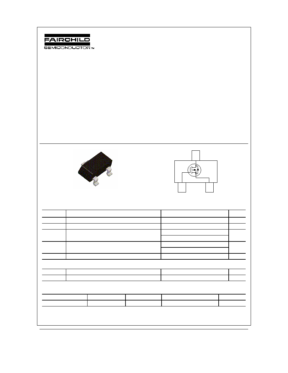
FDN5618P
60V P-Channel Logic Level PowerTrench
MOSFET
General Description
This 60V P-Channel MOSFET uses Fairchild's high
voltage PowerTrench process. It has been optimized for
power management applications.
Applications
· DC-DC converters
· Load switch
· Power management
Features
· 1.25 A, 60 V. R
DS(ON)
= 0.170
@ V
GS
= 10 V
R
DS(ON)
= 0.230
@ V
GS
= 4.5 V
· Fast switching speed
· High performance trench technology for extremely
low R
DS(ON)
G
D
S
SuperSOT -3
TM
D
S
G
Absolute Maximum Ratings
T
A
=25
o
C unless otherwise noted
Symbol
Parameter
Ratings
Units
V
DSS
Drain-Source Voltage
60
V
V
GSS
Gate-Source Voltage
±20
V
I
D
Drain Current Continuous
(Note 1a)
1.25
A
Pulsed
10
Maximum Power Dissipation
(Note 1a)
0.5
P
D
(Note 1b)
0.46
W
T
J
, T
STG
Operating and Storage Junction Temperature Range
55 to +150
°C
Thermal Characteristics
R
JA
Thermal Resistance, Junction-to-Ambient
(Note 1a)
250
°C/W
R
JC
Thermal Resistance, Junction-to-Case
(Note 1)
75
°C/W
Package Marking and Ordering Information
Device Marking
Device
Reel Size
Tape width
Quantity
618
FDN5618P
7''
8mm
3000 units
F
DN56
18P
FDN5618P Rev B(W)
Electrical Characteristics
T
A
= 25°C unless otherwise noted
Symbol
Parameter
Test Conditions
Min
Typ Max Units
Off Characteristics
BV
DSS
DrainSource Breakdown Voltage
V
GS
= 0 V, I
D
= 250
µA
-60
V
BV
DSS
===T
J
Breakdown Voltage Temperature
Coefficient
I
D
= 250
µA,Referenced to 25°C
58
mV/
°C
I
DSS
Zero Gate Voltage Drain Current
V
DS
= 48 V,
V
GS
= 0 V
1
µA
I
GSSF
GateBody Leakage, Forward
V
GS
= 20V,
V
DS
= 0 V
100
nA
I
GSSR
GateBody Leakage, Reverse
V
GS
= 20 V
V
DS
= 0 V
100
nA
On Characteristics
(Note 2)
V
GS(th)
Gate Threshold Voltage
V
DS
= V
GS
, I
D
= 250
µA
1
1.6
3
V
V
GS(th)
===T
J
Gate Threshold Voltage
Temperature Coefficient
I
D
= 250
µA,Referenced to 25°C
4
mV/
°C
R
DS(on)
Static DrainSource
OnResistance
V
GS
= 10 V,
I
D
= 1.25 A
V
GS
= 4.5 V,
I
D
= 1.0 A
V
GS
= 10 V, I
D
= 3 A T
J
=125
°C
0.148
0.185
0.245
0.170
0.230
0.315
I
D(on)
OnState Drain Current
V
GS
= 10 V,
V
DS
= 5 V
5
A
g
FS
Forward Transconductance
V
DS
= 5 V,
I
D
= 1.25 A
4.3
S
Dynamic Characteristics
C
iss
Input Capacitance
430
pF
C
oss
Output Capacitance
52
pF
C
rss
Reverse Transfer Capacitance
V
DS
= 30 V,
V
GS
= 0 V,
f = 1.0 MHz
19
pF
Switching Characteristics
(Note 2)
t
d(on)
TurnOn Delay Time
6.5
13
ns
t
r
TurnOn Rise Time
8
16
ns
t
d(off)
TurnOff Delay Time
16.5
30
ns
t
f
TurnOff Fall Time
V
DD
= 30 V,
I
D
= 1 A,
V
GS
= 10 V,
R
GEN
= 6
4
8
ns
Q
g
Total Gate Charge
8.6
13.8
nC
Q
gs
GateSource Charge
1.5
nC
Q
gd
GateDrain Charge
V
DS
= 30 V,
I
D
= 1.25 A,
V
GS
= 10 V
1.3
nC
DrainSource Diode Characteristics and Maximum Ratings
I
S
Maximum Continuous DrainSource Diode Forward Current
0.42
A
V
SD
DrainSource Diode Forward
Voltage
V
GS
= 0 V,
I
S
= 0.42
(Note 2)
0.7
1.2
V
Notes:
1. R
JA
is the sum of the junction-to-case and case-to-ambient thermal resistance where the case thermal reference is defined as the solder mounting surface of
the drain pins. R
JC
is guaranteed by design while R
CA
is determined by the user's board design.
a) 250
°C/W when mounted on a
0.02 in
2
pad of 2 oz. copper.
b) 270°C/W when mounted on a
minimum pad.
Scale 1 : 1 on letter size paper
2. Pulse Test: Pulse Width
=300 µs, Duty Cycle =2.0
F
DN56
18P
FDN5618P Rev B(W)
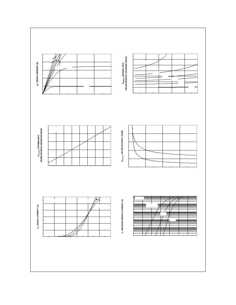
Typical Characteristics
0
1
2
3
4
5
0
1
2
3
4
-V
DS
, DRAIN-SOURCE VOLTAGE (V)
-4.5V
-6.0V
-2.5V
-4.0V
-3.5V
V
GS
= -10V
-3.0V
0.8
1
1.2
1.4
1.6
1.8
2
2.2
0
1
2
3
4
5
-I
D
, DRAIN CURRENT (A)
V
GS
= -3.0V
-4.0V
-10V
-4.5V
-6.0V
-3.5V
Figure 1. On-Region Characteristics.
Figure 2. On-Resistance Variation with
Drain Current and Gate Voltage.
0.8
0.9
1
1.1
1.2
1.3
-50
-25
0
25
50
75
100
125
150
T
J
, JUNCTION TEMPERATURE (
o
C)
I
D
= -1.25A
V
GS
= -10V
0.1
0.2
0.3
0.4
0.5
0.6
2
4
6
8
10
-V
GS
, GATE TO SOURCE VOLTAGE (V)
I
D
= -0.65 A
T
A
= 125
o
C
T
A
= 25
o
C
Figure 3. On-Resistance Variation
withTemperature.
Figure 4. On-Resistance Variation with
Gate-to-Source Voltage.
0
1
2
3
4
5
6
1
1.5
2
2.5
3
3.5
4
-V
GS
, GATE TO SOURCE VOLTAGE (V)
T
A
= 125
o
C
25
o
C
V
DS
= - 5V
-55
o
C
0.0001
0.001
0.01
0.1
1
10
0
0.2
0.4
0.6
0.8
1
1.2
1.4
-V
SD
, BODY DIODE FORWARD VOLTAGE (V)
T
A
= 125
o
C
25
o
C
-55
o
C
V
GS
= 0V
Figure 5. Transfer Characteristics.
Figure 6. Body Diode Forward Voltage Variation
with Source Current and Temperature.
F
DN56
18P
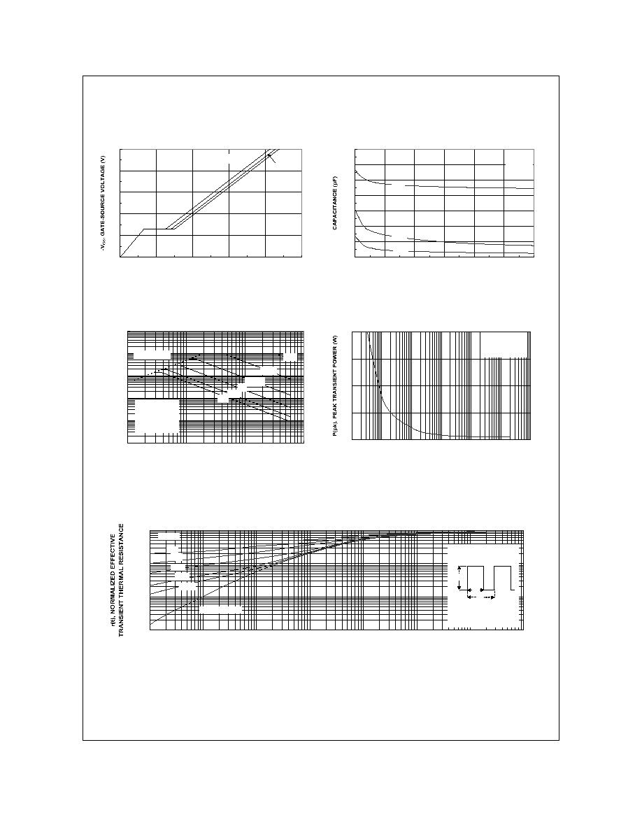
FDN5618P Rev B(W)
Typical Characteristics
0
2
4
6
8
10
0
2
4
6
8
10
Q
g
, GATE CHARGE (nC)
I
D
= -1.25A
V
DS
= -20V
-40V
-30V
0
100
200
300
400
500
600
700
0
2
4
6
8
10
12
-V
DS
, DRAIN TO SOURCE VOLTAGE (V)
C
ISS
C
RSS
C
OSS
f = 1MHz
V
GS
= 0 V
Figure 7. Gate Charge Characteristics.
Figure 8. Capacitance Characteristics.
0.001
0.01
0.1
1
10
100
0.1
1
10
100
-V
DS
, DRAIN-SOURCE VOLTAGE (V)
-I
D
, DRAIN CURRE
NT (
A
)
DC
10s
1s
100ms
R
DS(ON)
LIMIT
V
GS
=-10V
SINGLE PULSE
R
JA
= 270
o
C/W
T
A
= 25
o
C
10ms
1ms
0
5
10
15
20
0.001
0.01
0.1
1
10
100
1000
t
1
, TIME (sec)
SINGLE PULSE
R
JA
= 270°C/W
T
A
= 25°C
Figure 9. Maximum Safe Operating Area.
Figure 10. Single Pulse Maximum
Power Dissipation.
0.001
0.01
0.1
1
0.0001
0.001
0.01
0.1
1
10
100
1000
t
1
, TIME (sec)
R
JA
(t) = r(t) + R
JA
R
JA
= 270 °C/W
T
J
- T
A
= P * R
JA
(t)
Duty Cycle, D = t
1
/ t
2
P(pk)
t
1
t
2
SINGLE PULSE
0.01
0.02
0.05
0.1
0.2
D = 0.5
Figure 11. Transient Thermal Response Curve.
Thermal characterization performed using the conditions described in Note 1b.
Transient thermal response will change depending on the circuit board design.
F
DN56
18P
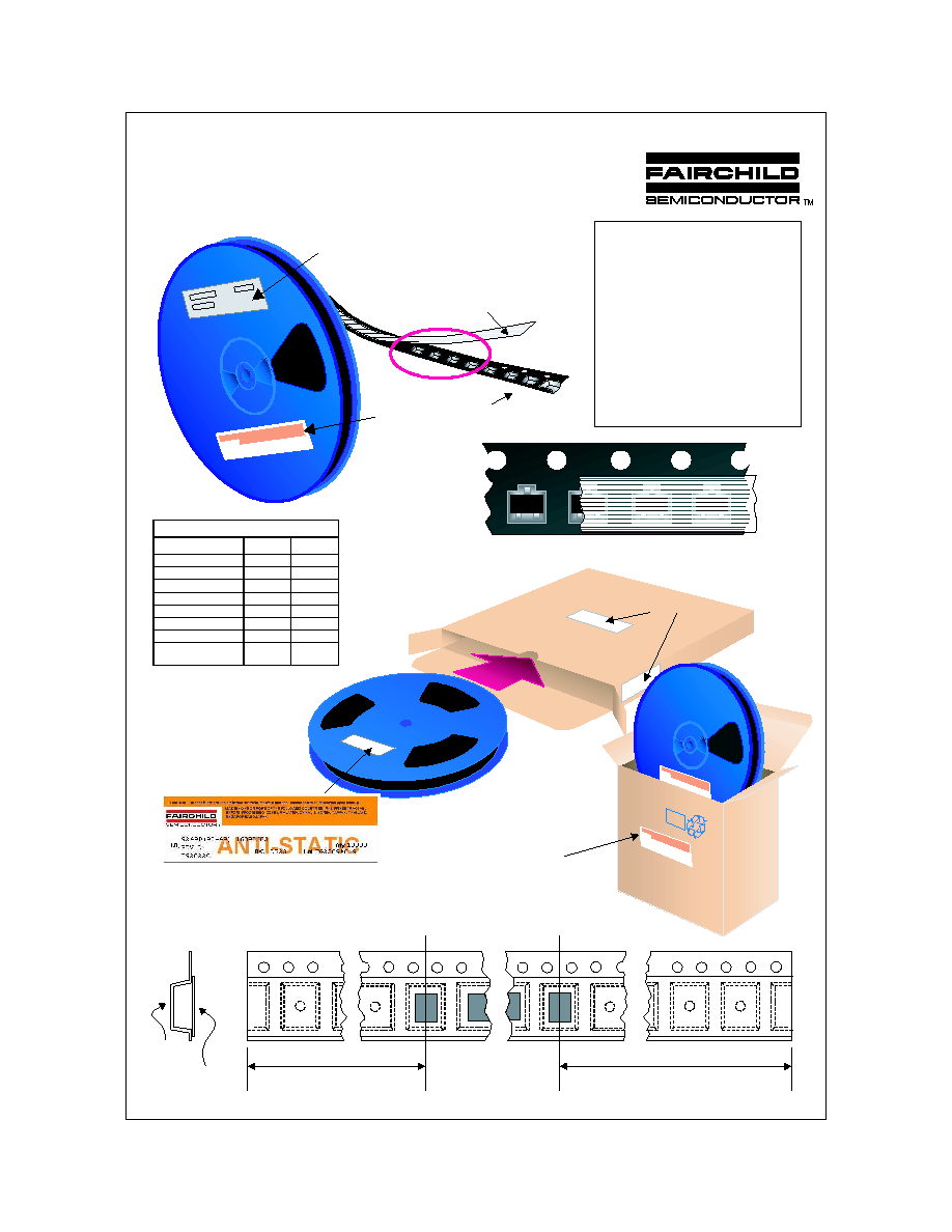
SSOT-3 Packaging
Configuration: Figure 1.0
Components
Leader Tape
500mm minimum or
125 empty pockets
Trailer Tape
300mm minimum or
75 empty pockets
SSOT-3 Tape Leader and Trailer
Configuration: Figure 2.0
Cover Tape
Carrier Tape
Note/Comments
Packaging Option
SSOT-3 Std Packaging Information
Standard
(no flow code)
D87Z
Packaging type
Reel Size
TNR
7" Dia
TNR
13"
Qty per Reel/Tube/Bag
3,000
10,000
Box Dimension (mm)
187x107x183 343x343x64
Max qty per Box
24,000
30,000
Weight per unit (gm)
0.0097
0.0097
Weight per Reel (kg)
0.1230
0.4150
Human Readable Label
Human Readable Label sample
343mm x 342mm x 64mm
Intermediate box for D87Z Option
Human Readable
Label
187mm x 107mm x 183mm
Intermediate Box for Standard Option
SSOT-3 Std Unit Orientation
3P
3P
3P
3P
Customize Label
Human Readable
Label
Embossed
Carrier Tape
Antistatic Cover Tape
Packaging Description:
SSOT-3 parts are shipped in tape. The carrier tape is
made from a dissipative (carbon filled) polycarbonate
resin. The cover tape is a multilayer film (Heat Activated
Adhesive in nature) primarily composed of polyester film,
adhesive layer, sealant, and anti-static sprayed agent.
These reeled parts in standard option are shipped with
3,000 units per 7" or 177cm diameter reel. The reels are
dark blue in color and is made of polystyrene plastic (anti-
static coated). Other option comes in 10,000 units per 13"
or 330cm diameter reel. This and some other options are
described in the Packaging Information table.
These full reels are individually labeled and placed inside
a standard intermediate made of recyclable corrugated
brown paper with a Fairchild logo printing. One pizza box
contains eight reels maximum. And these intermediate
boxes are placed inside a labeled shipping box which
comes in different sizes depending on the number of parts
shipped.
SuperSOT
TM
-3 Tape and Reel Data and Package Dimensions
August 1999, Rev. C
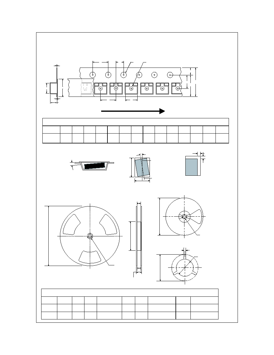
Dimensions are in millimeter
Pkg type
A0
B0
W
D0
D1
E1
E2
F
P1
P0
K0
T
Wc
Tc
SSOT-3
(8mm)
3.15
+/-0.10
2.77
+/-0.10
8.0
+/-0.3
1.55
+/-0.05
1.125
+/-0.125
1.75
+/-0.10
6.25
min
3.50
+/-0.05
4.0
+/-0.1
4.0
+/-0.1
1.30
+/-0.10
0.228
+/-0.013
5.2
+/-0.3
0.06
+/-02
Dimensions are in inches and millimeters
Tape Size
Reel
Option
Dim A
Dim B
Dim C
Dim D
Dim N
Dim W1
Dim W2
Dim W3 (LSL-USL)
8mm
7" Dia
7.00
177.8
0.059
1.5
512 +0.020/-0.008
13 +0.5/-0.2
0.795
20.2
2.165
55
0.331 +0.059/-0.000
8.4 +1.5/0
0.567
14.4
0.311 0.429
7.9 10.9
8mm
13" Dia
13.00
330
0.059
1.5
512 +0.020/-0.008
13 +0.5/-0.2
0.795
20.2
4.00
100
0.331 +0.059/-0.000
8.4 +1.5/0
0.567
14.4
0.311 0.429
7.9 10.9
See detail AA
Dim A
max
13" Diameter Option
7" Diameter Option
Dim A
Max
See detail AA
W3
W2 max Measured at Hub
W1 Measured at Hub
Dim N
Dim D
min
Dim C
B Min
DETAIL AA
Notes: A0, B0, and K0 dimensions are determined with respect to the EIA/Jedec RS-481
rotational and lateral movement requirements (see sketches A, B, and C).
20 deg maximum component rotation
0.5mm
maximum
0.5mm
maximum
Sketch C (Top View)
Component lateral movement
Typical
component
cavity
center line
20 deg maximum
Typical
component
center line
B0
A0
Sketch B (Top View)
Component Rotation
Sketch A (Side or Front Sectional View)
Component Rotation
User Direction of Feed
SSOT-3 Embossed Carrier Tape
Configuration: Figure 3.0
SSOT-3 Reel Configuration: Figure 4.0
P1
A0
D1
F
W
E1
E2
Tc
Wc
K0
T
B0
D0
P0
P2
SuperSOT
TM
-3 Tape and Reel Data and Package Dimensions, continued
July 1999, Rev. C
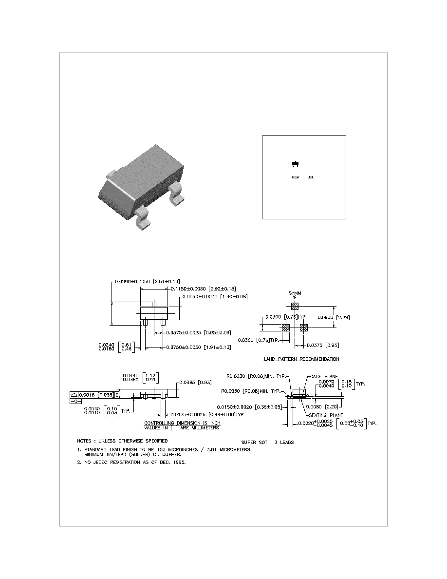
SuperSOT
TM
-3 (FS PKG Code 32)
1 : 1
Scale 1:1 on letter size paper
Di mensions shown below are in:
inches [mil limeters]
Part Weight per unit (gram): 0.0097
SuperSOT
TM
-3 Tape and Reel Data and Package Dimensions, continued
September 1998, Rev. A
TRADEMARKS
ACExTM
BottomlessTM
CoolFETTM
CROSSVOLTTM
E
2
CMOS
TM
FACTTM
FACT Quiet SeriesTM
FAST
FASTrTM
GTOTM
The following are registered and unregistered trademarks Fairchild Semiconductor owns or is authorized to use and is
not intended to be an exhaustive list of all such trademarks.
LIFE SUPPORT POLICY
FAIRCHILD'S PRODUCTS ARE NOT AUTHORIZED FOR USE AS CRITICAL COMPONENTS IN LIFE SUPPORT
DEVICES OR SYSTEMS WITHOUT THE EXPRESS WRITTEN APPROVAL OF FAIRCHILD SEMICONDUCTOR CORPORATION.
As used herein:
1. Life support devices or systems are devices or
systems which, (a) are intended for surgical implant into
the body, or (b) support or sustain life, or (c) whose
failure to perform when properly used in accordance
with instructions for use provided in the labeling, can be
reasonably expected to result in significant injury to the
user.
2. A critical component is any component of a life
support device or system whose failure to perform can
be reasonably expected to cause the failure of the life
support device or system, or to affect its safety or
effectiveness.
PRODUCT STATUS DEFINITIONS
Definition of Terms
Datasheet Identification
Product Status
Definition
Advance Information
Preliminary
No Identification Needed
Obsolete
This datasheet contains the design specifications for
product development. Specifications may change in
any manner without notice.
This datasheet contains preliminary data, and
supplementary data will be published at a later date.
Fairchild Semiconductor reserves the right to make
changes at any time without notice in order to improve
design.
This datasheet contains final specifications. Fairchild
Semiconductor reserves the right to make changes at
any time without notice in order to improve design.
This datasheet contains specifications on a product
that has been discontinued by Fairchild semiconductor.
The datasheet is printed for reference information only.
Formative or
In Design
First Production
Full Production
Not In Production
DISCLAIMER
FAIRCHILD SEMICONDUCTOR RESERVES THE RIGHT TO MAKE CHANGES WITHOUT FURTHER
NOTICE TO ANY PRODUCTS HEREIN TO IMPROVE RELIABILITY, FUNCTION OR DESIGN. FAIRCHILD
DOES NOT ASSUME ANY LIABILITY ARISING OUT OF THE APPLICATION OR USE OF ANY PRODUCT
OR CIRCUIT DESCRIBED HEREIN; NEITHER DOES IT CONVEY ANY LICENSE UNDER ITS PATENT
RIGHTS, NOR THE RIGHTS OF OTHERS.
SuperSOTTM-8
SyncFETTM
TinyLogicTM
UHCTM
VCXTM
HiSeCTM
ISOPLANARTM
MICROWIRETM
POPTM
PowerTrench
QFETTM
QSTM
Quiet SeriesTM
SuperSOTTM-3
SuperSOTTM-6
Rev. E