 | ÐлекÑÑоннÑй компоненÑ: FDP2552 | СкаÑаÑÑ:  PDF PDF  ZIP ZIP |
Äîêóìåíòàöèÿ è îïèñàíèÿ www.docs.chipfind.ru
©2002 Fairchild Semiconductor Corporation
October 2002
FDB2552 / FDP2552
Rev. B
FD
B
2
5
52 /
F
D
P
255
2
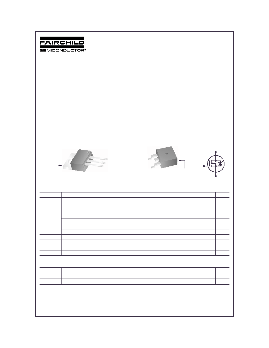
FDB2552 / FDP2552
N-Channel PowerTrench
®
MOSFET
150V, 37A, 36m
Features
· r
DS(ON)
= 32m
(Typ.), V
GS
= 10V, I
D
= 16A
· Q
g
(tot) = 39nC (Typ.), V
GS
= 10V
· Low Miller Charge
· Low Q
RR
Body Diode
· UIS Capability (Single Pulse and Repetitive Pulse)
· Qualified to AEC Q101
Formerly developmental type 82869
Applications
· DC/DC Converters and Off-line UPS
· Distributed Power Architectures and VRMs
· Primary Switch for 24V and 48V Systems
· High Voltage Synchronous Rectifier
· Direct Injection / Diesel Injection Systems
· 42V Automotive Load Control
· Electronic Valve Train Systems
MOSFET Maximum Ratings
T
C
= 25°C unless otherwise noted
Thermal Characteristics
This product has been designed to meet the extreme test conditions and environment demanded by the automotive industry. For a
copy of the requirements, see AEC Q101 at: http://www.aecouncil.com/
Reliability data can be found at: http://www.fairchildsemi.com/products/discrete/reliability/index.html.
All Fairchild Semiconductor products are manufactured, assembled and tested under ISO9000 and QS9000 quality systems
certification.
Symbol
Parameter
Ratings
Units
V
DSS
Drain to Source Voltage
150
V
V
GS
Gate to Source Voltage
±
20
V
I
D
Drain Current
37
A
Continuous (T
C
= 25
o
C, V
GS
= 10V)
Continuous (T
C
= 100
o
C, V
GS
= 10V)
26
A
Continuous (T
amb
= 25
o
C, V
GS
= 10V) with R
JA
= 43
o
C/W
5
A
Pulsed
Figure 4
A
E
AS
Single Pulse Avalanche Energy (Note 1)
390
mJ
P
D
Power dissipation
150
W
Derate above 25
o
C
1.0
W/
o
C
T
J
, T
STG
Operating and Storage Temperature
-55 to 175
o
C
R
JC
Thermal Resistance Junction to Case TO-220, TO-263
1.0
o
C/W
R
JA
Thermal Resistance Junction to Ambient TO-220, TO-263 (Note 2)
62
o
C/W
R
JA
Thermal Resistance Junction to Ambient TO-263, 1in
2
copper pad area
43
o
C/W
D
G
S
TO-263AB
FDB SERIES
GATE
SOURCE
DRAIN
(FLANGE)
TO-220AB
FDP SERIES
DRAIN
DRAIN
GATE
SOURCE
(FLANGE)
©2002 Fairchild Semiconductor Corporation
FDB2552 / FDP2552 Rev. B
FD
B
2
5
52 /
F
D
P
255
2
Package Marking and Ordering Information
Electrical Characteristics
T
C
= 25°C unless otherwise noted
Off Characteristics
On Characteristics
Dynamic Characteristics
Switching Characteristics
(V
GS
= 10V)
Drain-Source Diode Characteristics
Notes:
1: Starting T
J
= 25°C, L = 7.8mH, I
AS
= 10A.
2: Pulse Width = 100s
Device Marking
Device
Package
Reel Size
Tape Width
Quantity
FDB2552
FDB2552
TO-263AB
330mm
24mm
800 units
FDP2552
FDP2552
TO-220AB
Tube
N/A
50 units
Symbol
Parameter
Test Conditions
Min
Typ
Max
Units
B
VDSS
Drain to Source Breakdown Voltage
I
D
= 250
µ
A, V
GS
= 0V
150
-
-
V
I
DSS
Zero Gate Voltage Drain Current
V
DS
= 120V
-
-
1
µ
A
V
GS
= 0V
T
C
= 150
o
C
-
-
250
I
GSS
Gate to Source Leakage Current
V
GS
=
±
20V
-
-
±
100
nA
V
GS(TH)
Gate to Source Threshold Voltage
V
GS
= V
DS
, I
D
= 250
µ
A
2
-
4
V
r
DS(ON)
Drain to Source On Resistance
I
D
= 16A, V
GS
= 10V
-
0.032
0.036
I
D
= 8A, V
GS
= 6V
-
0.036
0.054
I
D
= 16A, V
GS
= 10V,
T
J
= 175
o
C
-
0.084
0.097
C
ISS
Input Capacitance
V
DS
= 25V, V
GS
= 0V,
f = 1MHz
-
2800
-
pF
C
OSS
Output Capacitance
-
285
-
pF
C
RSS
Reverse Transfer Capacitance
-
55
-
pF
Q
g(TOT)
Total Gate Charge at 10V
V
GS
= 0V to 10V
V
DD
= 75V
I
D
= 16A
I
g
= 1.0mA
39
51
nC
Q
g(TH)
Threshold Gate Charge
V
GS
= 0V to 2V
-
5.2
6.8
nC
Q
gs
Gate to Source Gate Charge
-
13.5
-
nC
Q
gs2
Gate Charge Threshold to Plateau
-
8.4
-
nC
Q
gd
Gate to Drain "Miller" Charge
-
8.3
-
nC
t
ON
Turn-On Time
V
DD
= 75V, I
D
= 16A
V
GS
= 10V, R
GS
= 8.2
-
-
62
ns
t
d(ON)
Turn-On Delay Time
-
12
-
ns
t
r
Rise Time
-
29
-
ns
t
d(OFF)
Turn-Off Delay Time
-
36
-
ns
t
f
Fall Time
-
29
-
ns
t
OFF
Turn-Off Time
-
-
97
ns
V
SD
Source to Drain Diode Voltage
I
SD
= 16A
-
-
1.25
V
I
SD
= 8A
-
-
1.0
V
t
rr
Reverse Recovery Time
I
SD
= 16A, dI
SD
/dt = 100A/
µ
s
-
-
90
ns
Q
RR
Reverse Recovered Charge
I
SD
= 16A, dI
SD
/dt = 100A/
µ
s
-
-
242
nC
©2002 Fairchild Semiconductor Corporation
FDB2552 / FDP2552 Rev. B
FD
B
2
5
52 /
F
D
P
255
2
Typical Characteristics
T
C
= 25°C unless otherwise noted
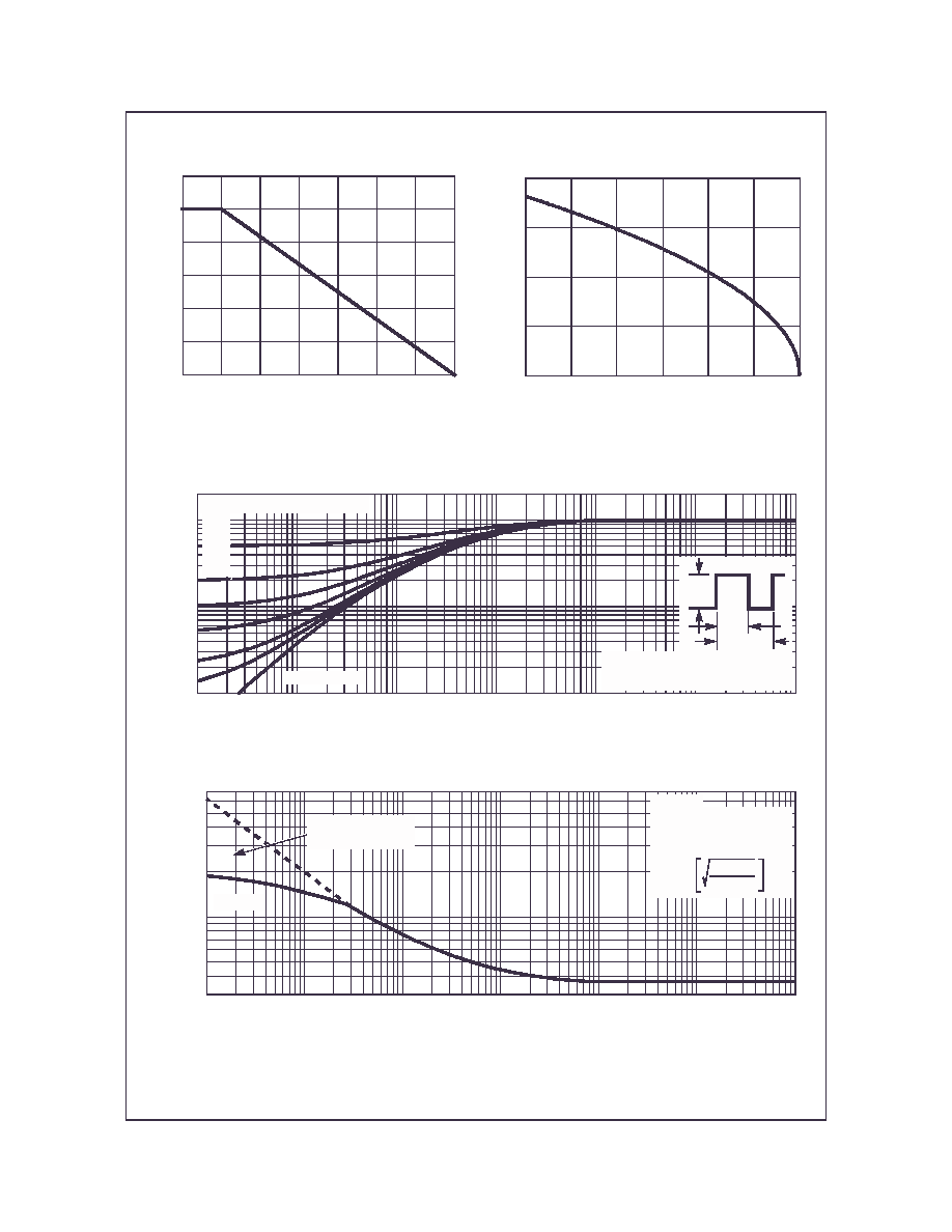
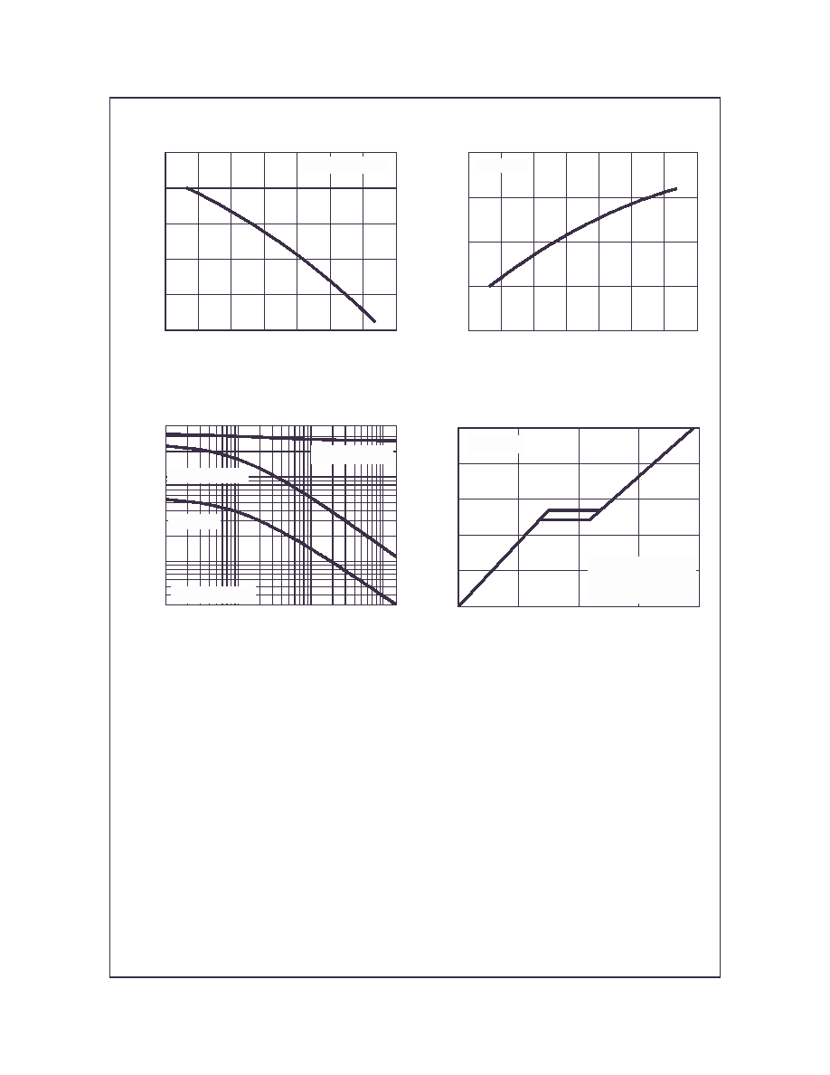
Figure 1. Normalized Power Dissipation vs
Ambient Temperature
Figure 2. Maximum Continuous Drain Current vs
Case Temperature
Figure 3. Normalized Maximum Transient Thermal Impedance
Figure 4. Peak Current Capability
T
C
, CASE TEMPERATURE (
o
C)
PO
WE
R
D
I
SSI
P
A
T
I
O
N
M
U
L
T
I
P
L
I
ER
0
0
25
50
75
100
175
0.2
0.4
0.6
0.8
1.0
1.2
125
150
0
10
20
30
40
25
50
75
100
125
150
175
I
D
, DRAIN CUR
RE
NT
(
A
)
T
C
, CASE TEMPERATURE (
o
C)
0.1
1
10
-5
10
-4
10
-3
10
-2
10
-1
10
0
10
1
0.01
2
t , RECTANGULAR PULSE DURATION (s)
Z
JC
, NO
RM
AL
IZ
E
D
T
H
E
R
M
A
L
IM
P
E
D
ANCE
NOTES:
DUTY FACTOR: D = t
1
/t
2
PEAK T
J
= P
DM
x Z
JC
x R
JC
+ T
C
P
DM
t
1
t
2
0.5
0.2
0.1
0.05
0.01
0.02
DUTY CYCLE - DESCENDING ORDER
SINGLE PULSE
100
30
700
I
DM
, P
E
AK CUR
RE
NT
(
A
)
t, PULSE WIDTH (s)
10
-5
10
-4
10
-3
10
-2
10
-1
10
0
10
1
TRANSCONDUCTANCE
MAY LIMIT CURRENT
IN THIS REGION
V
GS
= 10V
T
C
= 25
o
C
I = I
25
175 - T
C
150
FOR TEMPERATURES
ABOVE 25
o
C DERATE PEAK
CURRENT AS FOLLOWS:
©2002 Fairchild Semiconductor Corporation
FDB2552 / FDP2552 Rev. B
FD
B
2
5
52 /
F
D
P
255
2
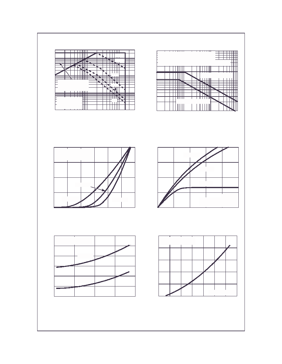
Figure 5. Forward Bias Safe Operating Area
NOTE: Refer to Fairchild Application Notes AN7514 and AN7515
Figure 6. Unclamped Inductive Switching
Capability
Figure 7. Transfer Characteristics
Figure 8. Saturation Characteristics
Figure 9. Drain to Source On Resistance vs Drain
Current
Figure 10. Normalized Drain to Source On
Resistance vs Junction Temperature
Typical Characteristics
T
C
= 25°C unless otherwise noted
DC
0.1
1
10
100
1
10
100
300
300
V
DS
, DRAIN TO SOURCE VOLTAGE (V)
I
D
, DRAIN CURRE
NT
(
A
)
T
J
= MAX RATED
T
C
= 25
o
C
SINGLE PULSE
LIMITED BY r
DS(ON)
AREA MAY BE
OPERATION IN THIS
1ms
100
µ
s
10
µ
s
10ms
1
10
100
0.1
1
10
0.01
I
AS
, A
V
AL
ANCHE
CURRE
NT
(
A
)
t
AV
, TIME IN AVALANCHE (ms)
STARTING T
J
= 25
o
C
STARTING T
J
= 150
o
C
t
AV
= (L)(I
AS
)/(1.3*RATED BV
DSS
- V
DD
)
If R = 0
If R
0
t
AV
= (L/R)ln[(I
AS
*R)/(1.3*RATED BV
DSS
- V
DD
) +1]
0
20
40
60
80
3.0
3.5
4.0
4.5
5.0
5.5
6.0
I
D
, DRAIN CURR
E
N
T
(
A
)
V
GS
, GATE TO SOURCE VOLTAGE (V)
PULSE DURATION = 80
µ
s
DUTY CYCLE = 0.5% MAX
V
DD
= 15V
T
J
= 175
o
C
T
J
= 25
o
C
T
J
= -55
o
C
0
20
40
60
80
0
1
2
3
4
5
I
D
, DRAIN CURRE
NT
(
A
)
V
DS
, DRAIN TO SOURCE VOLTAGE (V)
V
GS
= 6V
PULSE DURATION = 80
µ
s
DUTY CYCLE = 0.5% MAX
V
GS
= 5V
T
C
= 25
o
C
V
GS
= 10V
30
32
34
36
38
40
42
0
10
20
30
40
I
D
, DRAIN CURRENT (A)
V
GS
= 6V
V
GS
= 10V
D
RAIN T
O
S
O
URCE
O
N
RE
S
I
S
T
AN
CE
(
m
)
PULSE DURATION = 80
µ
s
DUTY CYCLE = 0.5% MAX
0.5
1.0
1.5
2.0
2.5
3.0
-80
-40
0
40
80
120
160
200
NO
RM
AL
IZ
E
D
DRAIN T
O
S
O
URCE
T
J
, JUNCTION TEMPERATURE (
o
C)
O
N
RE
S
I
S
T
ANCE
V
GS
= 10V, I
D
= 16A
PULSE DURATION = 80
µ
s
DUTY CYCLE = 0.5% MAX
©2002 Fairchild Semiconductor Corporation
FDB2552 / FDP2552 Rev. B
FD
B
2
5
52 /
F
D
P
255
2
Figure 11. Normalized Gate Threshold Voltage vs
Junction Temperature
Figure 12. Normalized Drain to Source
Breakdown Voltage vs Junction Temperature
Figure 13. Capacitance vs Drain to Source
Voltage
Figure 14. Gate Charge Waveforms for Constant
Gate Currents
Typical Characteristics
T
C
= 25°C unless otherwise noted
0.4
0.6
0.8
1.0
1.2
1.4
-80
-40
0
40
80
120
160
200
NO
RM
AL
IZ
E
D
G
A
T
E
T
J
, JUNCTION TEMPERATURE (
o
C)
V
GS
= V
DS
, I
D
= 250
µ
A
T
HRE
S
H
O
L
D V
O
L
T
A
G
E
0.8
0.9
1.0
1.1
1.2
-80
-40
0
40
80
120
160
200
T
J
, JUNCTION TEMPERATURE (
o
C)
NO
RM
AL
IZ
E
D
DRAIN T
O
S
O
UR
CE
I
D
= 250
µ
A
BRE
AKDO
W
N
V
O
L
T
A
G
E
100
1000
0.1
1
10
150
10
4000
C, CAP
A
C
IT
AN
CE
(
p
F
)
V
DS
, DRAIN TO SOURCE VOLTAGE (V)
V
GS
= 0V, f = 1MHz
C
ISS
=
C
GS
+ C
GD
C
OSS
C
DS
+ C
GD
C
RSS
=
C
GD
0
2
4
6
8
10
0
10
20
30
40
V
GS
, G
A
T
E
T
O
S
O
URCE
V
O
L
T
A
G
E
(
V
)
Q
g
, GATE CHARGE (nC)
V
DD
= 75V
I
D
= 37A
I
D
= 16A
WAVEFORMS IN
DESCENDING ORDER: