 | ÐлекÑÑоннÑй компоненÑ: FDP2670 | СкаÑаÑÑ:  PDF PDF  ZIP ZIP |
Äîêóìåíòàöèÿ è îïèñàíèÿ www.docs.chipfind.ru
November 2001
2001 Fairchild Semiconductor Corporation
FDP2670/FDB2670 Rev C1(W)
FDP2670/FDB2670
200V N-Channel PowerTrench
MOSFET
General Description
This N-Channel MOSFET has been designed
specifically for switching on the primary side in the
isolated DC/DC converter application. Any application
requiring a 200V MOSFETs with low on-resistance and
fast switching will benefit.
These MOSFETs feature faster switching and lower
gate charge than other MOSFETs with comparable
RDS
(ON)
specifications.
The result is a MOSFET that is easy and safer to drive
(even at very high frequencies), and DC/DC power
supply designs with higher overall efficiency.
Features
·
19 A, 200 V.
R
DS(ON)
= 130 m
@ V
GS
= 10 V
·
Low gate charge (27 nC typical)
·
Fast switching speed
·
High performance trench technology for extremely
low R
DS(ON)
·
High power and current handling capability
S
G
D
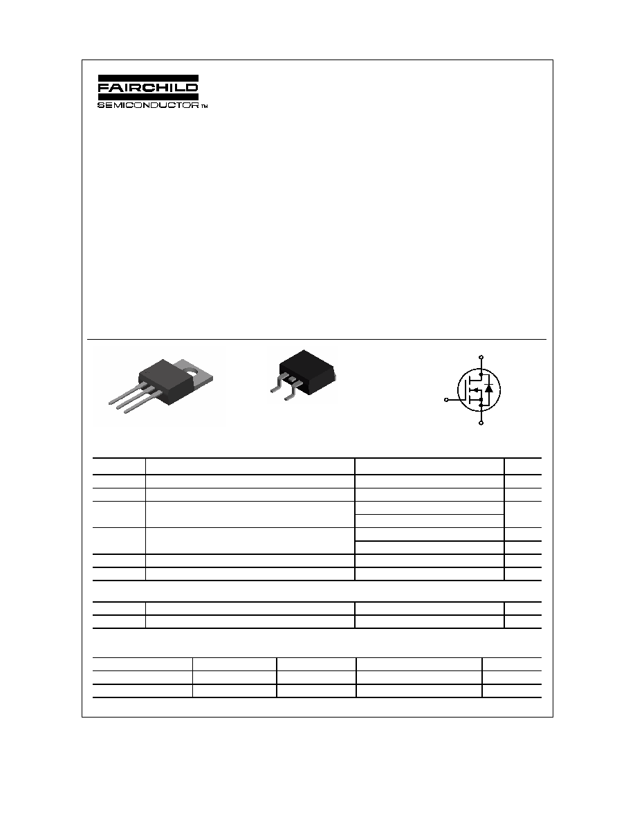
TO-220
FDP Series
D
G
S
TO-263AB
FDB Series
S
G
D
Absolute Maximum Ratings
T
A
=25
o
C unless otherwise noted
Symbol
Parameter
Ratings
Units
V
DSS
Drain-Source Voltage
200
V
V
GSS
Gate-Source Voltage
±
20
V
I
D
Drain Current Continuous
(Note 1)
19
A
Pulsed
(Note 1)
40
A
P
D
Total Power Dissipation @ T
C
= 25
°
C
93
W
Derate above 25
°
C
0.63
W
°
/C
dv/dt
Peak Diode Recovery dv/dt
(Note 3)
3.2
V/ns
T
J
, T
STG
Operating and Storage Junction Temperature Range
65 to +175
°
C
Thermal Characteristics
R
JC
Thermal Resistance, Junction-to-Case
1.6
°
C/W
R
JA
Thermal Resistance, Junction-to-Ambient
62.5
°
C/W
Package Marking and Ordering Information
Device Marking
Device
Reel Size
Tape width
Quantity
FDB2670
FDB2670
13''
24mm
800 units
FDP2670
FDP2670
Tube
n/a
45 units
FDP2670
/
FDB2670
FDP2670/FDB2670 Rev C1(W)
Electrical Characteristics
T
A
= 25°C unless otherwise noted
Symbol
Parameter
Test Conditions
Min
Typ Max Units
Drain-Source Avalanche Ratings
(Note 1)
W
DSS
Single Pulse Drain-Source
Avalanche Energy
V
DD
= 100 V,
I
D
= 10 A
375
mJ
I
AR
Maximum Drain-Source Avalanche
Current
10
A
Off Characteristics
BV
DSS
DrainSource Breakdown Voltage
V
GS
= 0 V, I
D
= 250
µ
A
200
V
BV
DSS
T
J
Breakdown Voltage Temperature
Coefficient
I
D
= 250
µ
A, Referenced to 25
°
C
241
mV/
°
C
I
DSS
Zero Gate Voltage Drain Current
V
DS
= 160 V,
V
GS
= 0 V
1
µ
A
I
GSSF
GateBody Leakage, Forward
V
GS
= 20 V,
V
DS
= 0 V
100
nA
I
GSSR
GateBody Leakage, Reverse
V
GS
= 20 V
V
DS
= 0 V
100
nA
On Characteristics
(Note 2)
V
GS(th)
Gate Threshold Voltage
V
DS
= V
GS
, I
D
= 250
µ
A
2
4
4.5
V
V
GS(th)
T
J
Gate Threshold Voltage
Temperature Coefficient
I
D
= 250
µ
A, Referenced to 25
°
C
9
mV/
°
C
R
DS(on)
Static DrainSource
OnResistance
V
GS
= 10 V,
I
D
= 10 A
V
GS
= 10V, I
D
= 10 A, T
J
= 125
°
C
98
205
130
285
m
I
D(on)
OnState Drain Current
V
GS
= 10 V,
V
DS
= 10 V
20
A
g
FS
Forward Transconductance
V
DS
= 10 V,
I
D
= 10 A
24
S
Dynamic Characteristics
C
iss
Input Capacitance
1320
pF
C
oss
Output Capacitance
71
pF
C
rss
Reverse Transfer Capacitance
V
DS
= 100 V,
V
GS
= 0 V,
f = 1.0 MHz
24
pF
Switching Characteristics
(Note 2)
t
d(on)
TurnOn Delay Time
14
25
ns
t
r
TurnOn Rise Time
5
10
ns
t
d(off)
TurnOff Delay Time
26
41
ns
t
f
TurnOff Fall Time
V
DD
= 100 V,
I
D
= 1 A,
V
GS
= 10 V,
R
GEN
= 6
23
37
ns
Q
g
Total Gate Charge
27
38
nC
Q
gs
GateSource Charge
7
nC
Q
gd
GateDrain Charge
V
DS
= 100 V,
I
D
= 10 A,
V
GS
= 10 V
10
nC
DrainSource Diode Characteristics and Maximum Ratings
I
S
Maximum Continuous DrainSource Diode Forward Current
19
A
V
SD
DrainSource Diode Forward
Voltage
V
GS
= 0 V,
I
S
= 10 A
(Note 2)
0.8
1.3
V
Notes:
1. Calculated continuous current based on maximum allowable junction temperature.
2. Pulse Test: Pulse Width < 300
µ
s, Duty Cycle < 2.0%
3. I
SD
3A, di/dt
100A/
µ
s, V
DD
BV
DSS
, Starting T
J
= 25
°
C
FDP2670
/
FDB2670
FDP2670/FDB2670 Rev C1(W)
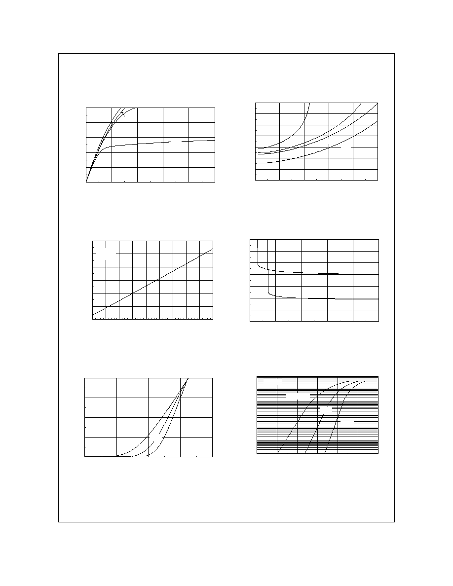
Typical Characteristics
0
6
12
18
24
30
0
3
6
9
12
15
V
DS
, DRAIN-SOURCE VOLTAGE (V)
I
D
, DRAIN CURRE
NT (
A
)
7.0V
6.0V
V
GS
= 10V
6.5V
0.8
0.9
1
1.1
1.2
1.3
1.4
1.5
0
6
12
18
24
30
I
D
, DRAIN CURRENT (A)
R
DS
(
O
N)
, NO
RMALIZE
D
DRAIN-
S
O
URCE
O
N
-
R
E
S
I
S
T
ANCE
V
GS
= 6V
6.5V
10V
7.0V
Figure 1. On-Region Characteristics.
Figure 2. On-Resistance Variation with
Drain Current and Gate Voltage.
0.2
0.6
1
1.4
1.8
2.2
2.6
-50
-25
0
25
50
75
100
125
150
175
T
J
, JUNCTION TEMPERATURE (
o
C)
R
DS
(
O
N)
, NO
RMALIZE
D
DRAIN-
S
O
URCE
O
N
-
R
E
S
I
S
T
ANC
E
I
D
=10A
V
GS
= 10V
0
0.05
0.1
0.15
0.2
0.25
0.3
0.35
5
6
7
8
9
10
V
GS
, GATE TO SOURCE VOLTAGE (V)
R
DS
(
O
N)
, O
N
-
R
E
S
I
S
T
ANCE
(
O
HM)
I
D
= 5A
T
A
= 125
o
C
T
A
= 25
o
C
Figure 3. On-Resistance Variation with
Temperature.
Figure 4. On-Resistance Variation with
Gate-to-Source Voltage.
0
10
20
30
40
3.5
4.5
5.5
6.5
7.5
V
GS
, GATE TO SOURCE VOLTAGE (V)
I
D
, DRAIN CURRE
NT (
A
)
T
A
= 125
o
C
25
o
C
-55
o
C
V
DS
= 50V
0.0001
0.001
0.01
0.1
1
10
100
0
0.2
0.4
0.6
0.8
1
1.2
V
SD
, BODY DIODE FORWARD VOLTAGE (V)
I
S
,
R
EVER
SE
DRAIN CURRE
NT (
A
)
T
A
= 125
o
C
25
o
C
-55
o
C
V
GS
= 0V
Figure 5. Transfer Characteristics.
Figure 6. Body Diode Forward Voltage Variation
with Source Current and Temperature.
FDP2670
/
FDB2670
FDP2670/FDB2670 Rev C1(W)
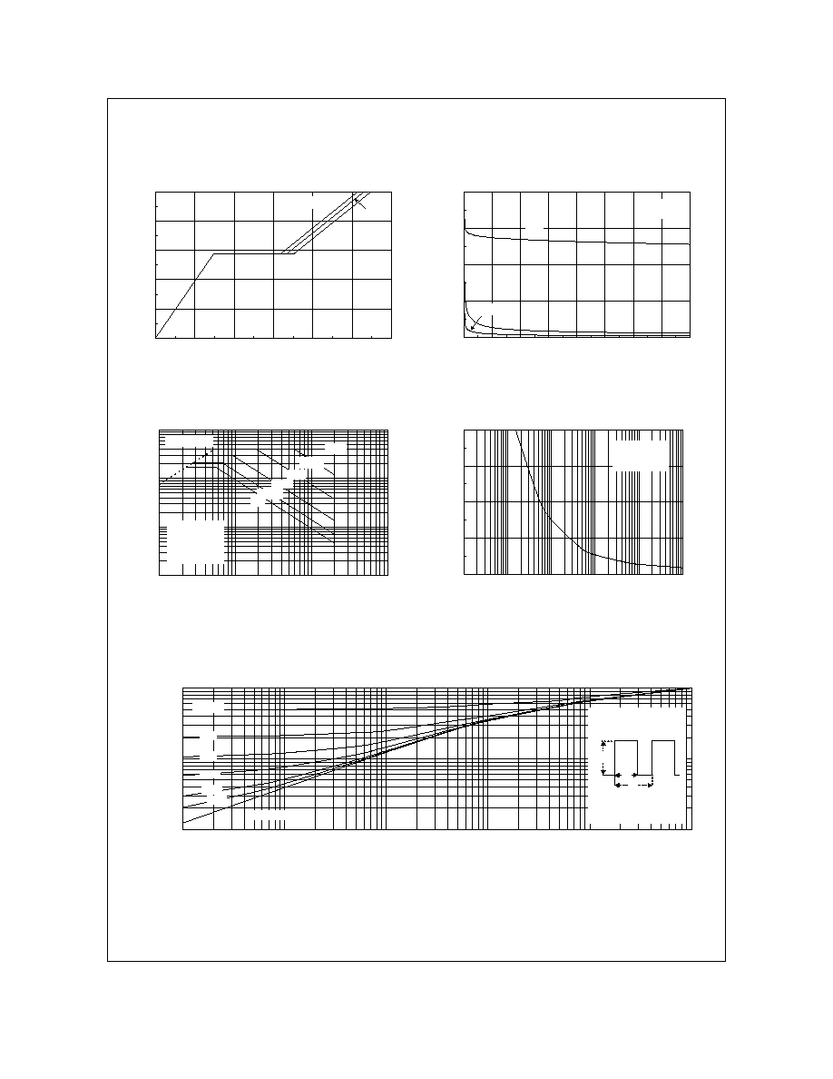
Typical Characteristics
0
2
4
6
8
10
0
5
10
15
20
25
30
Q
g
, GATE CHARGE (nC)
V
GS
, G
A
TE
-
S
O
URCE
V
O
LTAG
E
(
V
)
I
D
= 10A
V
DS
= 50V
100V
75V
0
500
1000
1500
2000
0
25
50
75
100
125
150
175
200
V
DS
, DRAIN TO SOURCE VOLTAGE (V)
CAP
ACITANCE
(
pF)
C
ISS
C
RSS
C
OSS
f = 1MHz
V
GS
= 0 V
Figure 7. Gate Charge Characteristics.
Figure 8. Capacitance Characteristics.
0.1
1
10
100
1
10
100
1000
V
DS
, DRAIN-SOURCE VOLTAGE (V)
I
D
, DRAIN CURRE
NT (
A
)
DC
100ms
R
DS(ON)
LIMIT
V
GS
= 10V
SINGLE PULSE
R
JC
= 1.6
o
C/W
T
C
= 25
o
C
10ms
1ms
100us
10us
0
500
1000
1500
2000
0.00001
0.0001
0.001
0.01
0.1
1
t
1
, TIME (sec)
P
(
pk
)
,
P
E
AK TRANS
IE
NT P
O
WE
R (
W
)
SINGLE PULSE
R
JC
= 1.6°C/W
T
C
= 25°C
Figure 9. Maximum Safe Operating Area.
Figure 10. Single Pulse Maximum
Power Dissipation.
0.01
0.1
1
0.00001
0.0001
0.001
0.01
0.1
1
t
1
, TIME (sec)
r
(t),
N
O
R
M
A
L
I
Z
ED
EFFEC
T
I
VE
T
RANS
IE
NT
T
H
E
R
M
A
L
RE
S
I
S
T
ANCE
R
JC
(t) = r(t) * R
JC
R
JC
= 1.6 °C/W
T
J
- T
C
= P * R
JC
(t)
Duty Cycle, D = t
1
/ t
2
P(pk)
t
1
t
2
SINGLE PULSE
0.01
0.02
0.05
0.1
0.2
D = 0.5
Figure 11. Transient Thermal Response Curve.
Thermal characterization performed using the conditions described in Note 1.
Transient thermal response will change depending on the circuit board design.
FDP2670
/
FDB2670

DISCLAIMER
FAIRCHILD SEMICONDUCTOR RESERVES THE RIGHT TO MAKE CHANGES WITHOUT FURTHER
NOTICE TO ANY PRODUCTS HEREIN TO IMPROVE RELIABILITY, FUNCTION OR DESIGN. FAIRCHILD
DOES NOT ASSUME ANY LIABILITY ARISING OUT OF THE APPLICATION OR USE OF ANY PRODUCT
OR CIRCUIT DESCRIBED HEREIN; NEITHER DOES IT CONVEY ANY LICENSE UNDER ITS PATENT
RIGHTS, NOR THE RIGHTS OF OTHERS.
TRADEMARKS
The following are registered and unregistered trademarks Fairchild Semiconductor owns or is authorized to use and is
not intended to be an exhaustive list of all such trademarks.
LIFE SUPPORT POLICY
FAIRCHILD'S PRODUCTS ARE NOT AUTHORIZED FOR USE AS CRITICAL COMPONENTS IN LIFE SUPPORT
DEVICES OR SYSTEMS WITHOUT THE EXPRESS WRITTEN APPROVAL OF FAIRCHILD SEMICONDUCTOR CORPORATION.
As used herein:
1. Life support devices or systems are devices or
systems which, (a) are intended for surgical implant into
the body, or (b) support or sustain life, or (c) whose
failure to perform when properly used in accordance
with instructions for use provided in the labeling, can be
reasonably expected to result in significant injury to the
user.
2. A critical component is any component of a life
support device or system whose failure to perform can
be reasonably expected to cause the failure of the life
support device or system, or to affect its safety or
effectiveness.
PRODUCT STATUS DEFINITIONS
Definition of Terms
Datasheet Identification
Product Status
Definition
Advance Information
Preliminary
No Identification Needed
Obsolete
This datasheet contains the design specifications for
product development. Specifications may change in
any manner without notice.
This datasheet contains preliminary data, and
supplementary data will be published at a later date.
Fairchild Semiconductor reserves the right to make
changes at any time without notice in order to improve
design.
This datasheet contains final specifications. Fairchild
Semiconductor reserves the right to make changes at
any time without notice in order to improve design.
This datasheet contains specifications on a product
that has been discontinued by Fairchild semiconductor.
The datasheet is printed for reference information only.
Formative or
In Design
First Production
Full Production
Not In Production
OPTOLOGICTM
OPTOPLANARTM
PACMANTM
POPTM
Power247TM
PowerTrench
QFETTM
QSTM
QT OptoelectronicsTM
Quiet SeriesTM
SILENT SWITCHER
FAST
FASTrTM
FRFETTM
GlobalOptoisolatorTM
GTOTM
HiSeCTM
ISOPLANARTM
LittleFETTM
MicroFETTM
MicroPakTM
MICROWIRETM
Rev. H4
®
ACExTM
BottomlessTM
CoolFETTM
CROSSVOLTTM
DenseTrenchTM
DOMETM
EcoSPARKTM
E
2
CMOS
TM
EnSigna
TM
FACTTM
FACT Quiet SeriesTM
SMART STARTTM
STAR*POWERTM
StealthTM
SuperSOTTM-3
SuperSOTTM-6
SuperSOTTM-8
SyncFETTM
TinyLogicTM
TruTranslationTM
UHCTM
UltraFET
®
®
®
STAR*POWER is used under license
VCXTM