 | –≠–ª–µ–∫—Ç—Ä–æ–Ω–Ω—ã–π –∫–æ–º–ø–æ–Ω–µ–Ω—Ç: FDP39N20 | –°–∫–∞—á–∞—Ç—å:  PDF PDF  ZIP ZIP |
©2005 Fairchild Semiconductor Corporation
1
www.fairchildsemi.com
FDP39N20 Rev. A
F
D
P39N20 200V N-Channel MOSFET
UniFET
TM
FDP39N20
200V N-Channel MOSFET
Features
∑ 39A, 300V, R
DS(on)
= 0.066
@V
GS
= 10 V
∑ Low gate charge ( typical 38 nC)
∑ Low C
rss
( typical 57 pF)
∑ Fast switching
∑ 100% avalanche tested
∑ Improved dv/dt capability
Description
These N-Channel enhancement mode power field effect transis-
tors are produced using Fairchild's proprietary, planar stripe,
DMOS technology.
This advanced technology has been especially tailored to mini-
mize on-state resistance, provide superior switching perfor-
mance, and withstand high energy pulse in the avalanche and
commutation mode. These devices are well suited for high effi-
cient switched mode power supplies and active power factor
correction.
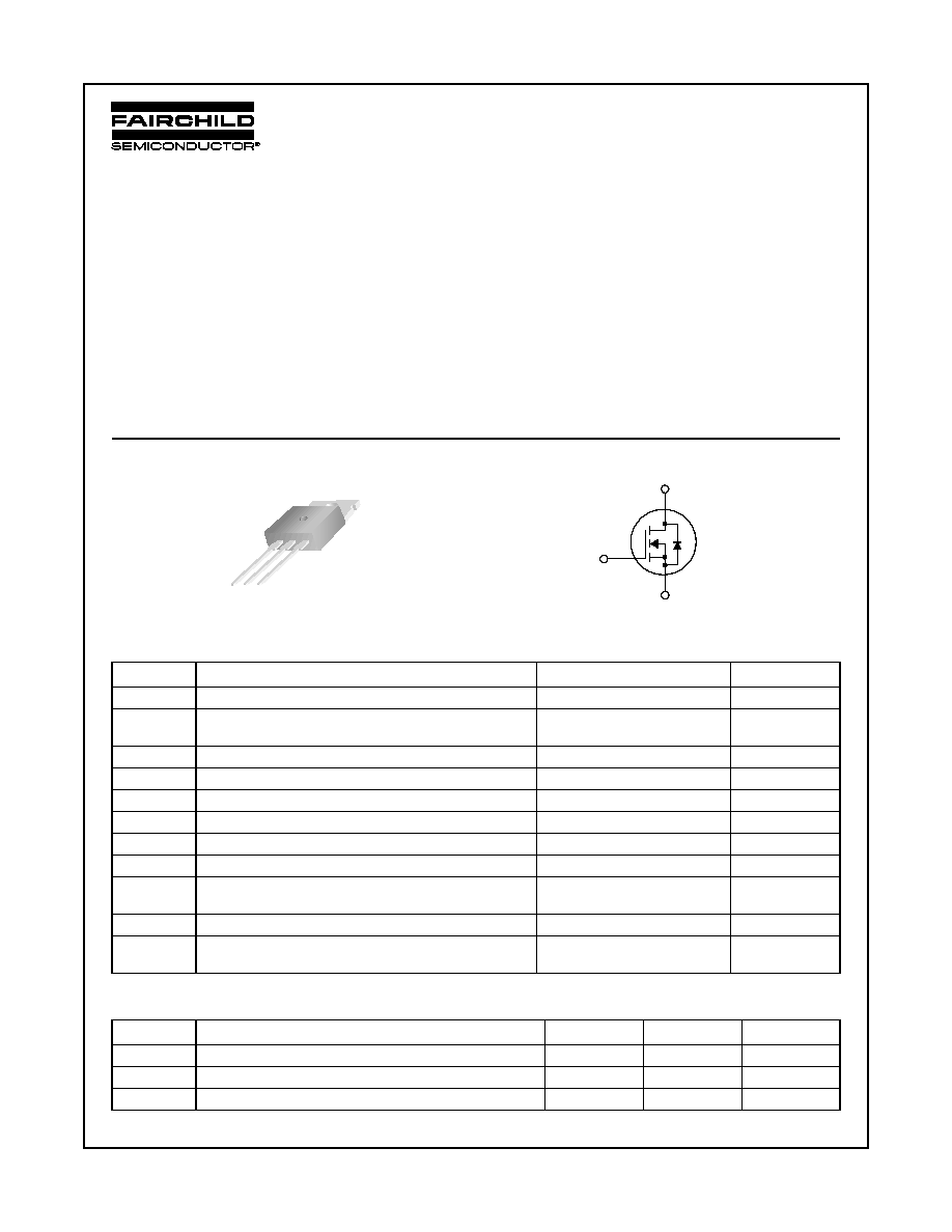
TO-220
FQP Series
G
S
D
D
G
S
Absolute Maximum Ratings
Symbol
Parameter
FDP39N20
Unit
V
DSS
Drain-Source Voltage
200
V
I
D
Drain Current
- Continuous (T
C
= 25
∞C)
- Continuous (T
C
= 100
∞C)
39
23.4
A
A
I
DM
Drain Current
- Pulsed
(Note 1)
156
A
V
GSS
Gate-Source voltage
±30
V
E
AS
Single Pulsed Avalanche Energy
(Note 2)
860
mJ
I
AR
Avalanche Current
(Note 1)
39
A
E
AR
Repetitive Avalanche Energy
(Note 1)
25.1
mJ
dv/dt
Peak Diode Recovery dv/dt
(Note 3)
4.5
V/ns
P
D
Power Dissipation
(T
C
= 25
∞C)
- Derate above 25
∞C
251
2.0
W
W/
∞C
T
J,
T
STG
Operating and Storage Temperature Range
-55 to +150
∞C
T
L
Maximum Lead Temperature for Soldering Purpose,
1/8" from Case for 5 Seconds
300
∞C
Thermal Characteristics
Symbol
Parameter
Min.
Max.
Unit
R
JC
Thermal Resistance, Junction-to-Case
--
0.50
∞C/W
R
CS
Thermal Resistance, Case-to-Sink
0.5
--
∞C/W
R
JA
Thermal Resistance, Junction-to-Ambient
--
62.5
∞C/W
2
www.fairchildsemi.com
FDP39N20 Rev. A
F
D
P39N20 200V N-Channel MOSFET
Package Marking and Ordering Information
Device Marking
Device
Package
Reel Size
Tape Width
Quantity
FDP39N20
FDP39N20
TO-220
-
-
50
Electrical Characteristics
T
C
= 25∞C unless otherwise noted
Symbol
Parameter
Conditions
Min.
Typ.
Max Units
Off Characteristics
BV
DSS
Drain-Source Breakdown Voltage
V
GS
= 0V, I
D
= 250
µA
200
--
--
V
BV
DSS
/
T
J
Breakdown Voltage Temperature
Coefficient
I
D
= 250
µA, Referenced to 25∞C
--
0.2
--
V/
∞C
I
DSS
Zero Gate Voltage Drain Current
V
DS
= 200V, V
GS
= 0V
V
DS
= 160V, T
C
= 125
∞C
--
--
--
--
1
10
µA
µA
I
GSSF
Gate-Body Leakage Current, Forward
V
GS
= 30V, V
DS
= 0V
--
--
100
nA
I
GSSR
Gate-Body Leakage Current, Reverse
V
GS
= -30V, V
DS
= 0V
--
--
-100
nA
On Characteristics
V
GS(th)
Gate Threshold Voltage
V
DS
= V
GS
, I
D
= 250
µA
3.0
--
5.0
V
R
DS(on)
Static Drain-Source
On-Resistance
V
GS
= 10V, I
D
= 19.5A
--
0.056
0.066
g
FS
Forward Transconductance
V
DS
= 40V, I
D
= 19.5A
(Note 4)
--
28.5
--
S
Dynamic Characteristics
C
iss
Input Capacitance
V
DS
= 25V, V
GS
= 0V,
f = 1.0MHz
--
1640
2130
pF
C
oss
Output Capacitance
--
400
520
pF
C
rss
Reverse Transfer Capacitance
--
57
85
pF
Switching Characteristics
t
d(on)
Turn-On Delay Time
V
DD
= 100V, I
D
= 39A
R
G
= 25
(Note 4, 5)
--
30
70
ns
t
r
Turn-On Rise Time
--
160
330
ns
t
d(off)
Turn-Off Delay Time
--
150
310
ns
t
f
Turn-Off Fall Time
--
150
310
ns
Q
g
Total Gate Charge
V
DS
= 160V, I
D
= 39A
V
GS
= 10V
(Note 4, 5)
--
38
49
nC
Q
gs
Gate-Source Charge
--
11
--
nC
Q
gd
Gate-Drain Charge
--
16.5
--
nC
Drain-Source Diode Characteristics and Maximum Ratings
I
S
Maximum Continuous Drain-Source Diode Forward Current
--
--
39
A
I
SM
Maximum Pulsed Drain-Source Diode Forward Current
--
--
156
A
V
SD
Drain-Source Diode Forward Voltage
V
GS
= 0V, I
S
= 39A
--
--
1.4
V
t
rr
Reverse Recovery Time
V
GS
= 0V, I
S
= 39A
dI
F
/dt =100A/
µs
(Note 4)
--
152
--
ns
Q
rr
Reverse Recovery Charge
--
1.1
--
µC
NOTES:
1. Repetitive Rating: Pulse width limited by maximum junction temperature
2. L = 0.85mH, I
AS
= 39A, V
DD
= 50V, R
G
= 25
, Starting T
J
= 25
∞C
3. I
SD
39A, di/dt 200A/µs, V
DD
BV
DSS
, Starting T
J
= 25
∞C
4. Pulse Test: Pulse width
300µs, Duty Cycle 2%
5. Essentially Independent of Operating Temperature Typical Characteristics
3
www.fairchildsemi.com
FDP39N20 Rev. A
F
D
P39N20 200V N-Channel MOSFET
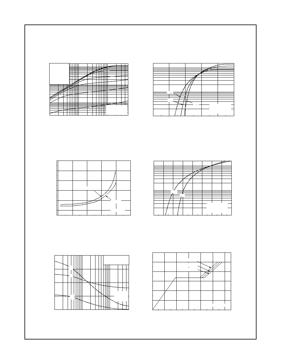
Typical Performance Characteristics
Figure 1. On-Region Characteristics
Figure 2. Transfer Characteristics
Figure 3. On-Resistance Variation vs.
Figure 4. Body Diode Forward Voltage
Drain Current and Gate Voltage
Variation vs. Source Current
and Temperatue
Figure 5. Capacitance Characteristics
Figure 6. Gate Charge Characteristics
10
-1
10
0
10
1
10
0
10
1
10
2
V
GS
Top : 15.0 V
10.0 V
8.0 V
7.0 V
6.5 V
6.0 V
Bottom : 5.5 V
Notes :
1. 250s Pulse Test
2. T
C
= 25
I
D
, D
r
ai
n
Cu
r
r
en
t [A
]
V
DS
, Drain-Source Voltage [V]
2
4
6
8
10
12
10
0
10
1
10
2
150
o
C
25
o
C
-55
o
C
Notes :
1. V
DS
= 40V
2. 250s Pulse Test
I
D
,
Dr
ai
n C
u
r
r
e
n
t
[
A
]
V
GS
, Gate-Source Voltage [V]
0
25
50
75
100
125
0.04
0.06
0.08
0.10
0.12
0.14
V
GS
= 20V
V
GS
= 10V
Note : T
J
= 25
R
DS
(O
N
)
[
],
D
r
ai
n-S
o
urc
e
On
-
R
es
is
t
a
nc
e
I
D
, Drain Current [A]
0.2
0.4
0.6
0.8
1.0
1.2
1.4
1.6
1.8
10
0
10
1
10
2
150
Notes :
1. V
GS
= 0V
2. 250s Pulse Test
25
I
DR
,
Re
v
e
r
s
e D
r
ain C
u
r
r
e
nt
[
A
]
V
SD
, Source-Drain voltage [V]
10
-1
10
0
10
1
0
2000
4000
C
iss
= C
gs
+ C
gd
(C
ds
= shorted)
C
oss
= C
ds
+ C
gd
C
rss
= C
gd
Note ;
1. V
GS
= 0 V
2. f = 1 MHz
C
rss
C
oss
C
iss
Capac
it
anc
es [
p
F]
V
DS
, Drain-Source Voltage [V]
0
10
20
30
40
50
60
0
2
4
6
8
10
12
V
DS
= 100V
V
DS
= 40V
V
DS
= 160V
Note : I
D
= 39A
V
GS
,
G
a
t
e
-
S
ou
r
c
e Vol
t
ag
e [
V
]
Q
G
, Total Gate Charge [nC]

4
www.fairchildsemi.com
FDP39N20 Rev. A
F
D
P39N20 200V N-Channel MOSFET
Typical Performance Characteristics
(Continued)
Figure 7. Breakdown Voltage Variation
Figure 8. On-Resistance Variation
vs. Temperature
vs. Temperature
Figure 9. Maximum Safe Operating Area
Figure 10. Maximum Drain Current
vs. Case Temperature
Figure 11. Transient Thermal Response Curve
-100
-50
0
50
100
150
200
0.8
0.9
1.0
1.1
1.2
Notes :
1. V
GS
= 0 V
2. I
D
= 250 A
BV
DS
S
,
(Nor
m
a
liz
e
d
)
D
r
ai
n-S
o
urce B
r
e
a
kd
ow
n
V
o
l
t
age
T
J
, Junction Temperature [
o
C]
-100
-50
0
50
100
150
200
0.0
0.5
1.0
1.5
2.0
2.5
3.0
Notes :
1. V
GS
= 10 V
2. I
D
= 19.5 A
R
DS
(O
N)
, (N
ormal
i
z
ed)
Dr
ain
-
S
o
u
r
ce
O
n
-R
es
ista
nc
e
T
J
, Junction Temperature [
o
C]
10
0
10
1
10
2
10
-2
10
-1
10
0
10
1
10
2
10
3
100 ms
1 ms
10
µ
s
DC
10 ms
100
µ
s
Operation in This Area
is Limited by R
DS(on)
Notes :
1. T
C
= 25
o
C
2. T
J
= 150
o
C
3. Single Pulse
I
D
,
Dr
a
i
n
C
u
r
r
e
nt
[A]
V
DS
, Drain-Source Voltage [V]
25
50
75
100
125
150
0
10
20
30
40
I
D
,
Dr
ain Cur
r
ent
[
A
]
T
C
, Case Temperature [ ]
1 0
-5
1 0
-4
1 0
-3
1 0
-2
1 0
-1
1 0
0
1 0
1
1 0
-2
1 0
-1
N o te s :
1 . Z
J C
( t) = 0 .5 /W M a x .
2 . D u ty F a c to r , D = t
1
/t
2
3 . T
J M
- T
C
= P
D M
* Z
J C
( t)
s in g le p u ls e
D = 0 .5
0 .0 2
0 .2
0 .0 5
0 .1
0 .0 1
Z
JC
(
t
), Therma
l R
e
spo
n
se
t
1
, S q u a re W a v e P u ls e D u r a tio n [s e c ]
t
1
P
DM
t
2

5
www.fairchildsemi.com
FDP39N20 Rev. A
F
D
P39N20 200V N-Channel MOSFET
Gate Charge Test Circuit & Waveform
Resistive Switching Test Circuit & Waveforms
Unclamped Inductive Switching Test Circuit & Waveforms