 | ÐлекÑÑоннÑй компоненÑ: FDPF15N65 | СкаÑаÑÑ:  PDF PDF  ZIP ZIP |
Äîêóìåíòàöèÿ è îïèñàíèÿ www.docs.chipfind.ru
©2006 Fairchild Semiconductor Corporation
1
www.fairchildsemi.com
FDP15N65 / FDPF15N65 Rev. A
F
D
P15N65 / FDPF15N65 650V N-Ch
annel MOSFET
February 2006
UniFET
TM
FDP15N65 / FDPF15N65
650V N-Channel MOSFET
Features
· 15A, 650V, R
DS(on)
= 0.44
@V
GS
= 10 V
· Low gate charge ( typical 48.5 nC)
· Low C
rss
( typical 23.6 pF)
· Fast switching
· 100% avalanche tested
· Improved dv/dt capability
Description
These N-Channel enhancement mode power field effect transis-
tors are produced using Fairchild's proprietary, planar stripe,
DMOS technology.
This advanced technology has been especially tailored to mini-
mize on-state resistance, provide superior switching perfor-
mance, and withstand high energy pulse in the avalanche and
commutation mode. These devices are well suited for high effi-
cient switched mode power supplies and active power factor
correction.
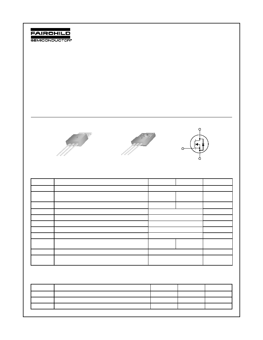
TO-220
FDP Series
G
S
D
TO-220F
FDPF Series
G
S
D
D
G
S
Absolute Maximum Ratings
Symbol
Parameter
FDP15N65 FDPF15N65
Unit
V
DSS
Drain-Source Voltage
650
V
I
D
Drain Current
- Continuous (T
C
= 25
°C)
- Continuous (T
C
= 100
°C)
15
9.5
15*
9.5*
A
A
I
DM
Drain Current
- Pulsed
(Note 1)
60
60*
A
V
GSS
Gate-Source voltage
± 30
V
E
AS
Single Pulsed Avalanche Energy
(Note 2)
637
mJ
I
AR
Avalanche Current
(Note 1)
15
A
E
AR
Repetitive Avalanche Energy
(Note 1)
25.0
mJ
dv/dt
Peak Diode Recovery dv/dt
(Note 3)
4.5
V/ns
P
D
Power Dissipation
(T
C
= 25
°C)
- Derate above 25
°C
250
2.0
73.5
0.59
W
W/
°C
T
J,
T
STG
Operating and Storage Temperature Range
-55 to +150
°C
T
L
Maximum Lead Temperature for Soldering Purpose,
1/8" from Case for 5 Seconds
300
°C
Thermal Characteristics
Symbol
Parameter
FDP15N65
FDPF15N65
Unit
R
JC
Thermal Resistance, Junction-to-Case
0.5
1.7
°C/W
R
CS
Thermal Resistance, Case-to-Sink
0.5
--
°C/W
R
JA
Thermal Resistance, Junction-to-Ambient
62.5
62.5
°C/W
* Drain current limited by maximum junction termperature.
2
www.fairchildsemi.com
FDP15N65 / FDPF15N65 Rev. A
F
D
P15N65 / FDPF15N65 650V N-Ch
annel MOSFET
Package Marking and Ordering Information
Device Marking
Device
Package
Reel Size
Tape Width
Quantity
FDP15N65
FDP15N65
TO-220
--
--
50
FDPF15N65
FDPF15N65
TO-220F
--
--
50
Electrical Characteristics
T
C
= 25°C unless otherwise noted
Symbol
Parameter
Conditions
Min
Typ
Max Units
Off Characteristics
BV
DSS
Drain-Source Breakdown Voltage
V
GS
= 0V, I
D
= 250
µA, T
J
= 25
°C
650
--
--
V
BV
DSS
/
T
J
Breakdown Voltage Temperature
Coefficient
I
D
= 250
µA, Referenced to 25°C
--
0.65
--
V/
°C
I
DSS
Zero Gate Voltage Drain Current
V
DS
= 650V, V
GS
= 0V
V
DS
= 520V, T
C
= 125
°C
--
--
--
--
1
10
µA
µA
I
GSSF
Gate-Body Leakage Current, Forward
V
GS
= 30V, V
DS
= 0V
--
--
100
nA
I
GSSR
Gate-Body Leakage Current, Reverse
V
GS
= -30V, V
DS
= 0V
--
--
-100
nA
On Characteristics
V
GS(th)
Gate Threshold Voltage
V
DS
= V
GS
, I
D
= 250
µA
3.0
--
5.0
V
R
DS(on)
Static Drain-Source
On-Resistance
V
GS
= 10V, I
D
= 7.5A
--
0.36
0.44
g
FS
Forward Transconductance
V
DS
= 40V, I
D
= 7.5A
(Note 4)
--
19.2
--
S
Dynamic Characteristics
C
iss
Input Capacitance
V
DS
= 25V, V
GS
= 0V,
f = 1.0MHz
--
2380
3095
pF
C
oss
Output Capacitance
--
295
385
pF
C
rss
Reverse Transfer Capacitance
--
23.6
35.5
pF
Switching Characteristics
t
d(on)
Turn-On Delay Time
V
DD
= 325V, I
D
= 15A
R
G
= 21.7
(Note 4, 5)
--
65
140
ns
t
r
Turn-On Rise Time
--
125
260
ns
t
d(off)
Turn-Off Delay Time
--
105
220
ns
t
f
Turn-Off Fall Time
--
65
140
ns
Q
g
Total Gate Charge
V
DS
= 520V, I
D
= 15A
V
GS
= 10V
(Note 4, 5)
--
48.5
63.0
nC
Q
gs
Gate-Source Charge
--
14.0
--
nC
Q
gd
Gate-Drain Charge
--
21.2
--
nC
Drain-Source Diode Characteristics and Maximum Ratings
I
S
Maximum Continuous Drain-Source Diode Forward Current
--
--
15
A
I
SM
Maximum Pulsed Drain-Source Diode Forward Current
--
--
60
A
V
SD
Drain-Source Diode Forward Voltage
V
GS
= 0V, I
S
= 15A
--
--
1.4
V
t
rr
Reverse Recovery Time
V
GS
= 0V, I
S
= 15A
dI
F
/dt =100A/
µs
(Note 4)
--
496
--
ns
Q
rr
Reverse Recovery Charge
--
5.69
--
µC
NOTES:
1. Repetitive Rating: Pulse width limited by maximum junction temperature
2. L = 5.23mH, I
AS
= 15A, V
DD
= 50V, R
G
= 25
, Starting T
J
= 25
°C
3. I
SD
15A, di/dt 200A/µs, V
DD
BV
DSS
, Starting T
J
= 25
°C
4. Pulse Test: Pulse width
300µs, Duty Cycle 2%
5. Essentially Independent of Operating Temperature Typical Characteristics
3
www.fairchildsemi.com
FDP15N65 / FDPF15N65 Rev. A
F
D
P15N65 / FDPF15N65 650V N-Ch
annel MOSFET
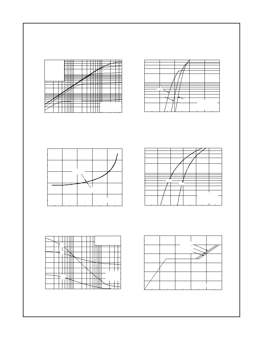
Typical Performance Characteristics
Figure 1. On-Region Characteristics
Figure 2. Transfer Characteristics
2
4
6
8
10
12
10
0
10
1
150
o
C
25
o
C
-55
o
C
Notes :
1. V
DS
= 40V
2. 250µ s Pulse Test
I
D
, D
r
a
i
n
C
u
rren
t
[A
]
V
GS
, Gate-Source Voltage [V]
10
-1
10
0
10
1
10
-1
10
0
10
1
V
GS
Top : 15.0 V
10.0 V
8.0 V
7.0 V
6.5 V
6.0 V
Bottom : 5.5 V
Notes :
1. 250µ s Pulse Test
2. T
C
= 25
I
D
,
Dr
ain
Cur
r
e
n
t
[
A
]
V
DS
, Drain-Source Voltage [V]
Figure 3. On-Resistance Variation vs.
Figure 4. Body Diode Forward Voltage
Drain Current and Gate Voltage
Variation vs. Source Current
and Temperatue
0
10
20
30
40
50
0.0
0.2
0.4
0.6
0.8
1.0
V
GS
= 20V
V
GS
= 10V
Note : T
J
= 25
R
DS(
O
N)
[
],
Drai
n-Sou
r
ce
O
n
-
R
esi
s
tan
c
e
I
D
, Drain Current [A]
0.2
0.4
0.6
0.8
1.0
1.2
1.4
10
0
10
1
150
Notes :
1. V
GS
= 0V
2. 250µ s Pulse Test
25
I
DR
,
Re
v
er
s
e Drai
n Cu
r
r
e
nt
[
A
]
V
SD
, Source-Drain voltage [V]
Figure 5. Capacitance Characteristics
Figure 6. Gate Charge Characteristics
0
10
20
30
40
50
0
2
4
6
8
10
12
V
DS
= 325V
V
DS
= 130V
V
DS
= 520V
Note : I
D
= 15A
V
GS
,
G
a
t
e
-Source V
o
lt
ag
e [
V
]
Q
G
, Total Gate Charge [nC]
10
-1
10
0
10
1
0
1000
2000
3000
4000
5000
C
iss
= C
gs
+ C
gd
(C
ds
= shorted)
C
oss
= C
ds
+ C
gd
C
rss
= C
gd
Note ;
1. V
GS
= 0 V
2. f = 1 MHz
C
rss
C
oss
C
iss
Cap
a
c
i
t
a
nc
es
[
p
F]
V
DS
, Drain-Source Voltage [V]
4
www.fairchildsemi.com
FDP15N65 / FDPF15N65 Rev. A
F
D
P15N65 / FDPF15N65 650V N-Ch
annel MOSFET
25
50
75
100
125
150
0
3
6
9
12
15
18
I
D
,
Drain C
u
rr
en
t
[
A
]
T
C
, Case Temperature [ ]
Typical Performance Characteristics
(Continued)
Figure 7. Breakdown Voltage Variation
Figure 8. On-Resistance Variation
vs. Temperature
vs. Temperature
-100
-50
0
50
100
150
200
0.8
0.9
1.0
1.1
1.2
Notes :
1. V
GS
= 0 V
2. I
D
= 250 µ A
BV
DS
S
, (N
o
r
m
a
l
i
z
e
d
)
D
r
ai
n-S
ource
B
r
eak
dow
n
Vol
t
a
g
e
T
J
, Junction Temperature [
o
C]
-100
-50
0
50
100
150
200
0.0
0.5
1.0
1.5
2.0
2.5
3.0
* Notes :
1. V
GS
= 10 V
2. I
D
= 5.5 A
R
DS
(O
N
)
,
(No
r
m
ali
z
ed)
D
r
ain-S
ource
O
n
-R
esist
a
nce
T
J
, Junction Temperature [
o
C]
-100
-50
0
50
100
150
200
0.0
0.5
1.0
1.5
2.0
2.5
3.0
Notes :
1. V
GS
= 10 V
2. I
D
= 7.5 A
R
DS
(
O
N)
,
(
N
or
m
al
i
z
e
d)
Drai
n-Sou
r
c
e On-Res
is
t
a
nc
e
T
J
, Junction Temperature [
o
C]
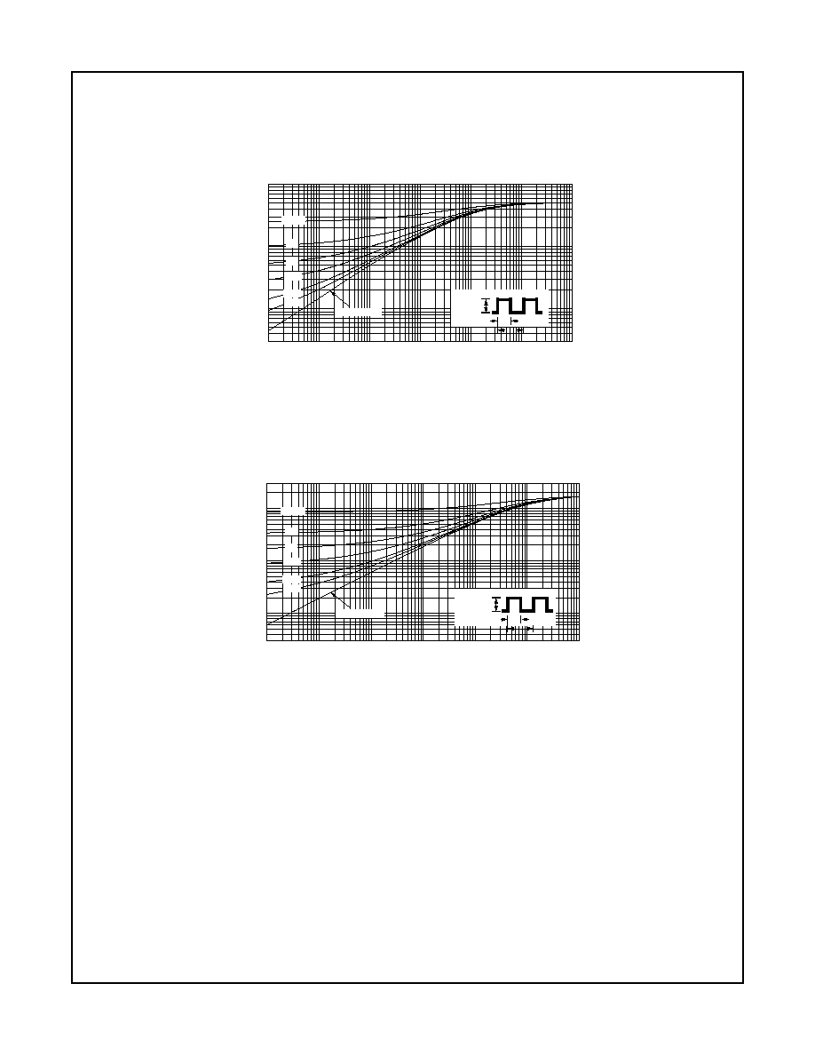
Figure 9-1. Safe Operating Area for FDP15N65 Figure 9-2. Safe Operating Area for FDPF15N65
10
0
10
1
10
2
10
3
10
-2
10
-1
10
0
10
1
10
2
100 ms
1 ms
10
µ
s
DC
10 ms
100
µ
s
Operation in This Area
is Limited by R
DS(on)
Notes :
1. T
C
= 25
o
C
2. T
J
= 150
o
C
3. Single Pulse
I
D
, Dra
i
n Cu
rr
en
t [A]
V
DS
, Drain-Source Voltage [V]
10
0
10
1
10
2
10
3
10
-2
10
-1
10
0
10
1
10
2
100 ms
1 ms
10
µ
s
DC
10 ms
100
µ
s
Operation in This Area
is Limited by R
DS(on)
Notes :
1. T
C
= 25
o
C
2. T
J
= 150
o
C
3. Single Pulse
I
D
, Dr
ai
n Curr
ent [A]
V
DS
, Drain-Source Voltage [V]
Figure 10. Maximum Drain Current vs. Case Temperature
5
www.fairchildsemi.com
FDP15N65 / FDPF15N65 Rev. A
F
D
P15N65 / FDPF15N65 650V N-Ch
annel MOSFET
Typical Performance Characteristics
(Continued)
Figure 11-1.
1 0
-5
1 0
-4
1 0
-3
1 0
-2
1 0
-1
1 0
0
1 0
1
1 0
-2
1 0
-1
1 0
0
N o te s :
1 . Z
J C
(t) = 0 .5
/W M a x .
2 . D u ty F a c to r, D = t
1
/t
2
3 . T
J M
- T
C
= P
D M
* Z
q J C
(t)
s in g le p u ls e
D = 0 .5
0 .0 2
0 .2
0 .0 5
0 .1
0 .0 1
Z
JC
(
t
),
Ther
mal Re
s
pon
s
e
t
1
, S q u a re W a v e P u ls e D u ra tio n [s e c ]
t
1
P
DM
t
2
Transient Thermal Response Curve for FDP15N65
Figure 11-2. Transient Thermal Response Curve for FDPF15N65
1 0
-5
1 0
-4
1 0
-3
1 0
-2
1 0
-1
1 0
0
1 0
1
1 0
-2
1 0
-1
1 0
0
N o te s :
1 . Z
J C
( t) = 1 .7
/W M a x .
2 . D u ty F a c to r, D = t
1
/t
2
3 . T
J M
- T
C
= P
D M
* Z
q J C
( t)
s in g le p u ls e
D = 0 .5
0 .0 2
0 .2
0 .0 5
0 .1
0 .0 1
Z
JC
(
t
)
,
T
her
mal
R
es
ponse
t
1
, S q u a re W a v e P u ls e D u ra tio n [s e c ]
t
1
P
DM
t
2
6
www.fairchildsemi.com
FDP15N65 / FDPF15N65 Rev. A
F
D
P15N65 / FDPF15N65 650V N-Ch
annel MOSFET
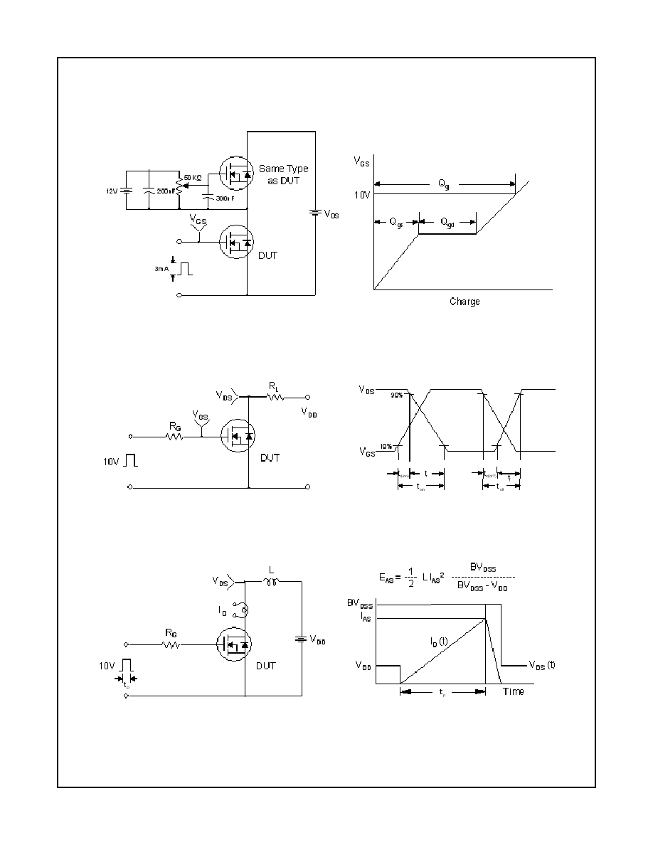
Gate Charge Test Circuit & Waveform
Resistive Switching Test Circuit & Waveforms
Unclamped Inductive Switching Test Circuit & Waveforms
7
www.fairchildsemi.com
FDP15N65 / FDPF15N65 Rev. A
F
D
P15N65 / FDPF15N65 650V N-Ch
annel MOSFET
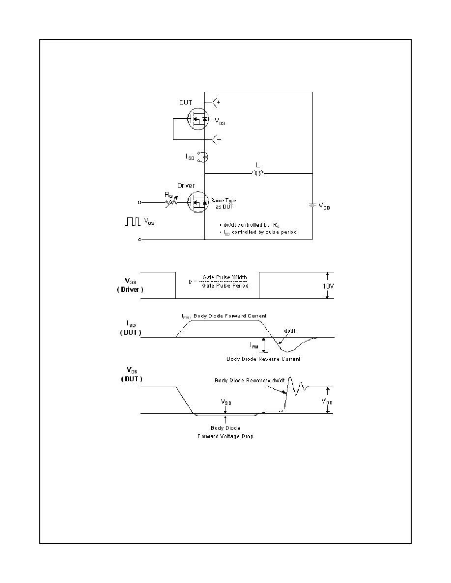
Peak Diode Recovery dv/dt Test Circuit & Waveforms
8
www.fairchildsemi.com
FDP15N65 / FDPF15N65 Rev. A
F
D
P15N65 / FDPF15N65 650V N-Ch
annel MOSFET
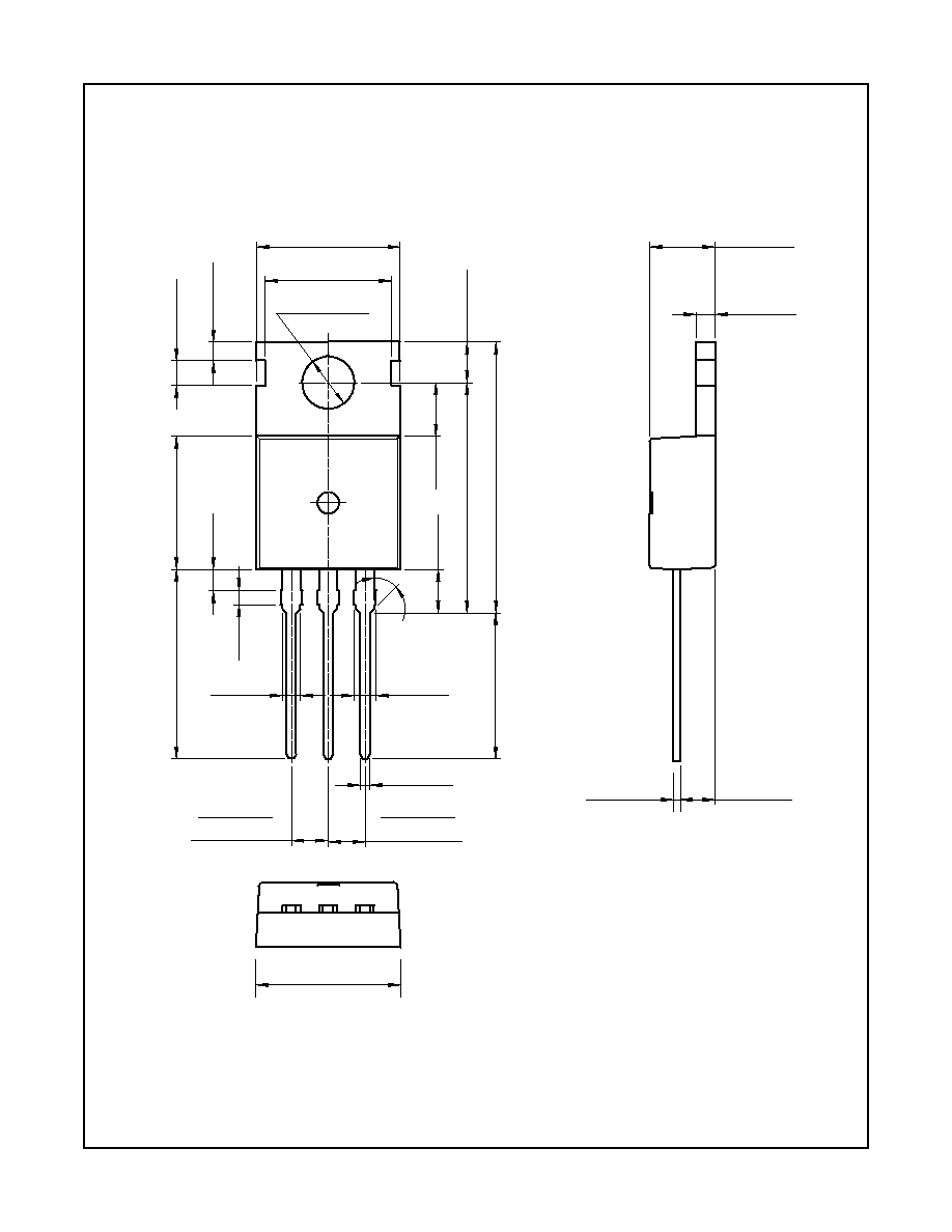
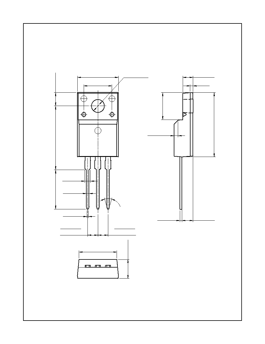
Mechanical Dimensions
4.50
±
0.20
9.90
±
0.20
1.52
±
0.10
0.80
±
0.10
2.40
±
0.20
10.00
±
0.20
1.27
±
0.10
ø3.60
±
0.10
(8.70)
2.80
±
0.10
15.90
±
0.20
10.08
±
0.30
18.95MAX.
(1.70)
(3.70)
(3.00)
(1.46)
(1.00)
(45
°
)
9.20
±
0.20
13.08
±
0.20
1.30
±
0.10
1.30
+0.10
0.05
0.50
+0.10
0.05
2.54TYP
[2.54
±
0.20
]
2.54TYP
[2.54
±
0.20
]
TO-220
Dimensions in Millimeters
9
www.fairchildsemi.com
FDP15N65 / FDPF15N65 Rev. A
F
D
P15N65 / FDPF15N65 650V N-Ch
annel MOSFET
Mechanical Dimensions
(Continued)
(7.00)
(0.70)
MAX1.47
(30
°
)
#1
3.30
±
0.1
0
15.80
±
0.20
15.87
±
0.20
6.68
±
0.20
9.75
±
0.30
4.70
±
0.20
10.16
±
0.20
(1.00x45
°
)
2.54
±
0.20
0.80
±
0.10
9.40
±
0.20
2.76
±
0.20
0.35
±
0.10
ø3.18
±
0.10
2.54TYP
[2.54
±
0.20
]
2.54TYP
[2.54
±
0.20
]
0.50
+0.10
0.05
TO-220F
Dimensions in Millimeters

10
www.fairchildsemi.com
FDP15N65 / FDPF15N65 Rev. A
F
D
P15N65 / FDPF15N65 650V N-Ch
annel MOSFET
TRADEMARKS
The following are registered and unregistered trademarks Fairchild Semiconductor owns or is authorized to use and is not
intended to be an exhaustive list of all such trademarks.
DISCLAIMER
FAIRCHILD SEMICONDUCTOR RESERVES THE RIGHT TO MAKE CHANGES WITHOUT FURTHER NOTICE TO ANY
PRODUCTS HEREIN TO IMPROVE RELIABILITY, FUNCTION OR DESIGN. FAIRCHILD DOES NOT ASSUME ANY
LIABILITY ARISING OUT OF THE APPLICATION OR USE OF ANY PRODUCT OR CIRCUIT DESCRIBED HEREIN;
NEITHER DOES IT CONVEY ANY LICENSE UNDER ITS PATENT RIGHTS, NOR THE RIGHTS OF OTHERS.
LIFE SUPPORT POLICY
FAIRCHILD'S PRODUCTS ARE NOT AUTHORIZED FOR USE AS CRITICAL COMPONENTS IN LIFE SUPPORT
DEVICES OR SYSTEMS WITHOUT THE EXPRESS WRITTEN APPROVAL OF FAIRCHILD SEMICONDUCTOR
CORPORATION.
As used herein:
1. Life support devices or systems are devices or systems
which, (a) are intended for surgical implant into the body, or
(b) support or sustain life, or (c) whose failure to perform
when properly used in accordance with instructions for use
provided in the labeling, can be reasonably expected to
result in significant injury to the user.
2. A critical component is any component of a life support
device or system whose failure to perform can be
reasonably expected to cause the failure of the life support
device or system, or to affect its safety or effectiveness.
PRODUCT STATUS DEFINITIONS
Definition of Terms
ACExTM
ActiveArrayTM
BottomlessTM
Build it NowTM
CoolFETTM
CROSSVOLTTM
DOMETM
EcoSPARKTM
E
2
CMOSTM
EnSignaTM
FACTTM
FACT Quiet SeriesTM
FAST
®
FASTrTM
FPSTM
FRFETTM
GlobalOptoisolatorTM
GTOTM
HiSeCTM
I
2
CTM
i-LoTM
ImpliedDisconnectTM
IntelliMAXTM
ISOPLANARTM
LittleFETTM
MICROCOUPLERTM
MicroFETTM
MicroPakTM
MICROWIRETM
MSXTM
MSXProTM
OCXTM
OCXProTM
OPTOLOGIC
®
OPTOPLANARTM
PACMANTM
POPTM
Power247TM
PowerEdgeTM
PowerSaverTM
PowerTrench
®
QFET
®
QSTM
QT OptoelectronicsTM
Quiet SeriesTM
RapidConfigureTM
RapidConnectTM
µSerDesTM
ScalarPumpTM
SILENT SWITCHER
®
SMART STARTTM
SPMTM
StealthTM
SuperFETTM
SuperSOTTM-3
SuperSOTTM-6
SuperSOTTM-8
SyncFETTM
TinyLogic
®
TINYOPTOTM
TruTranslationTM
UHCTM
UltraFET
®
UniFETTM
VCXTM
WireTM
Across the board. Around the world.TM
The Power Franchise
®
Programmable Active DroopTM
Datasheet Identification
Product Status
Definition
Advance Information
Formative or In
Design
This datasheet contains the design specifications for
product development. Specifications may change in
any manner without notice.
Preliminary
First Production
This datasheet contains preliminary data, and
supplementary data will be published at a later date.
Fairchild Semiconductor reserves the right to make
changes at any time without notice in order to improve
design.
No Identification Needed
Full Production
This datasheet contains final specifications. Fairchild
Semiconductor reserves the right to make changes at
any time without notice in order to improve design.
Obsolete
Not In Production
This datasheet contains specifications on a product
that has been discontinued by Fairchild semiconductor.
The datasheet is printed for reference information only.
Rev. I17
Document Outline