 | –≠–ª–µ–∫—Ç—Ä–æ–Ω–Ω—ã–π –∫–æ–º–ø–æ–Ω–µ–Ω—Ç: FDQ7238S | –°–∫–∞—á–∞—Ç—å:  PDF PDF  ZIP ZIP |

September 2003
©
2003 Fairchild Semiconductor Corporation
FDQ7238S Rev A1 (W)
FDQ7238S
Dual
Notebook
Power
Supply
N
-
Channel PowerTrench
in SO-14 Package
General Description
The FDQ7238S is designed to replace two single SO-8
MOSFETs in DC to DC power supplies. The high-side
switch (Q1) is designed with specific emphasis on
reducing switching losses while the low-side switch
(Q2) is optimized to reduce conduction losses using
Fairchild's SyncFET
TM
technology.
Features
∑
Q2
: 14 A, 30V. R
DS(on)
= 9.5 m
@ V
GS
= 10V
R
DS(on)
= 10.5 m
@ V
GS
= 4.5V
∑
Q1
: 11 A, 30V. R
DS(on)
= 14.5 m
@ V
GS
= 10V
R
DS(on)
= 16 m
@ V
GS
= 4.5V
SO-14
G1
G2
Vin
S2
S2
S2
Absolute Maximum Ratings
T
A
= 25∞C unless otherwise noted
Symbol
Parameter
Q2
Q1
Units
V
DSS
Drain-Source Voltage
30
30
V
V
GSS
Gate-Source Voltage
±
16
±
16
V
I
D
Drain Current - Continuous
(Note 1a)
14
11
A
- Pulsed
50
50
P
D
Power Dissipation for Single Operation
(Note 1a & 1b)
2.4
1.8
W
(Note 1c & 1d)
1.3
1.1
T
J
, T
STG
Operating and Storage Junction Temperature Range
-
55 to +150
∞
C
Thermal Characteristics
R
JA
Thermal Resistance, Junction-to-Ambient
(Note 1a & 1b)
52
68
∞
C/W
(Note 1c & 1d)
94
118
Package Marking and Ordering Information
Device Marking
Device
Reel Size
Tape width
Quantity
FDQ7238S
FDQ7238S
13"
16mm
2500 units
F
D
Q
7
2
3
8
S
pin 1
FDQ7238S Rev A1 (W)
Electrical Characteristics
T
A
= 25∞C unless otherwise noted
Symbol
Parameter
Test Conditions
Type
Min
Typ Max Units
Off Characteristics
BV
DSS
Drain-Source Breakdown Voltage V
GS
= 0 V,
I
D
= 1 mA
V
GS
= 0 V,
I
D
= 250
µ
A
Q2
Q1
30
30
V
BV
DSS
T
J
Breakdown Voltage Temperature
Coefficient
I
D
= 10 mA, Referenced to 25
∞
C
I
D
= 250
µ
A, Referenced to 25
∞
C
Q2
Q1
26
25
mV/
∞
C
I
DSS
Zero Gate Voltage Drain Current V
DS
= 24 V,
V
GS
= 0 V
Q2
Q1
500
1
µ
A
I
GSSF
Gate-Body Leakage, Forward
V
GS
= 16 V,
V
DS
= 0 V
Q2
Q1
100
100
nA
I
GSSR
Gate-Body Leakage, Reverse
V
GS
=
-
16 V, V
DS
= 0 V
Q2
Q1
-
100
-
100
nA
On Characteristics
(Note 2)
V
GS(th)
Gate Threshold Voltage
V
DS
= V
GS
,
I
D
= 1 mA
V
DS
= V
GS
,
I
D
= 250
µ
A
Q2
Q1
1
1
1.4
1.4
3
3
V
V
GS(th)
T
J
Gate Threshold Voltage
Temperature Coefficient
I
D
= 10 mA, Referenced to 25
∞
C
I
D
= 250
µ
A, Referenced to 25
∞
C
Q2
Q1
-
3
-
5
mV/
∞
C
R
DS(on)
Static Drain-Source
On-Resistance
V
GS
= 10 V,
I
D
= 14 A
V
GS
= 4.5 V,
I
D
= 13 A
V
GS
= 10 V, I
D
= 14A, T
J
= 125
∞
C
Q2
7
8
11
9.5
10.5
16
m
V
GS
= 10 V,
I
D
= 11 A
V
GS
= 4.5 V,
I
D
= 10 A
V
GS
= 10 V, I
D
= 11, T
J
= 125
∞
C
Q1
11
12
16
14.5
16
23
I
D(on)
On≠State Drain Current
V
GS
= 10 V,
V
DS
= 5 V
V
GS
= 10 V,
V
DS
= 5 V
Q2
Q1
50
50
A
g
FS
Forward Transconductance
V
DS
= 10 V,
I
D
= 14 A
V
DS
= 10 V,
I
D
= 11 A
Q2
Q1
67
48
S
Dynamic Characteristics
C
iss
Input Capacitance
Q2
Q1
2872
1906
pF
C
oss
Output Capacitance
Q2
Q1
522
311
pF
C
rss
Reverse Transfer Capacitance
V
DS
= 15 V,
V
GS
= 0 V,
f = 1.0 MHz
Q2
Q1
186
134
pF
R
G
Gate Resistance
V
GS
= 15 mVf = 1.0 MHz
Q2
1.5
Q1
0.8
Switching Characteristics
(Note 2)
t
d(on)
Turn-On Delay Time
Q2
Q1
14
11
25
20
nS
t
r
Turn-On Rise Time
Q2
Q1
13
13
23
23
nS
t
d(off)
Turn-Off Delay Time
Q2
Q1
51
28
82
45
nS
t
f
Turn-Off Fall Time
V
DD
= 15 V,
I
D
= 1 A,
V
GS
= 10V,
R
GEN
= 6
Q2
Q1
18
15
32
27
nS
Q
g
Total Gate Charge
Q2
Q1
48
33
67
46
nC
Q
gs
Gate-Source Charge
Q2
Q1
6
4
nC
Q
gd
Gate-Drain Charge
Q2
V
DS
= 15 V, I
D
= 14A, V
GS
= 10 V
Q1
V
DS
= 15 V, I
D
= 11A,V
GS
= 10 V
Q2
Q1
8
4
nC
F
D
Q
7
2
3
8
S
FDQ7238S Rev A1 (W)
Electrical Characteristics
T
A
= 25∞C unless otherwise noted
Symbol
Parameter
Test Conditions
Type
Min
Typ Max Units
Drain-Source Diode Characteristics and Maximum Ratings
I
S
Maximum Continuous Drain-Source Diode Forward Current
Q2
Q1
34
2.1
A
V
SD
Drain-Source Diode Forward
Voltage
V
GS
= 0 V,
I
S
= 3.4 A
(Note 2)
V
GS
= 0 V,
I
S
= 1.9 A
(Note 2)
Q2
0.44
0.37
0.7
V
V
GS
= 0 V,
I
S
= 2.1 A
(Note 2)
Q1
0.7
1.2
t
rr
Diode Reverse Recovery Time
Q2
26
nS
Q
rr
Diode Reverse Recovery Charge
I
F
= 14A
d
iF
/d
t
= 300 A/µs
22
nC
t
rr
Diode Reverse Recovery Time
Q1
25
nS
Q
rr
Diode Reverse Recovery Charge
I
F
= 11A
d
iF
/d
t
= 100 A/µs
14
nC
NOTE :
1.
R
JA
is the sum of the junction-to-case and case-to-ambient thermal resistance where the case thermal reference is defined as the solder mounting surface of
the drain pins. R
JC
is guaranteed by design while R
CA
is determined by the user's board design.
a)
68∞C/W when
mounted on a 1in
2
pad
of 2 oz copper (Q1).
b)
52∞C/W when
mounted on a 1in
2
pad
of 2 oz copper (Q2).
c)
118∞C/W when mounted
on a minimum pad of 2 oz
copper (Q1).
d)
94∞C/W when mounted on
a minimum pad of 2 oz
copper (Q2).
Scale 1 : 1 on letter size paper
2.
Pulse Test: Pulse Width < 300
µ
s, Duty Cycle < 2.0%
F
D
Q
7
2
3
8
S
FDQ7238S Rev A1 (W)
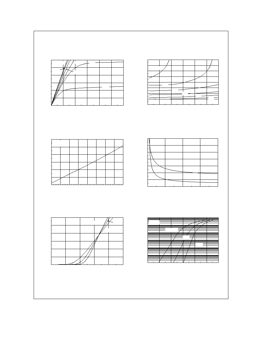
Typical Characteristics : Q2
0
10
20
30
40
50
60
0
0.5
1
1.5
2
V
DS
, DRAIN-SOURCE VOLTAGE (V)
I
D
,
D
R
A
I
N
C
U
R
R
E
N
T
(
A
)
2.5V
3.5V
V
GS
= 10V
4.5V
3.0V
6.0V
0.8
1
1.2
1.4
1.6
1.8
2
2.2
0
10
20
30
40
50
60
I
D
, DRAIN CURRENT (A)
R
D
S
(
O
N
)
,
N
O
R
M
A
L
I
Z
E
D
D
R
A
I
N
-
S
O
U
R
C
E
O
N
-
R
E
S
I
S
T
A
N
C
E
V
GS
= 2.5V
4.5V
3.0V
3.5V
10V
6.0V
Figure 1. On-Region Characteristics.
Figure 2. On-Resistance Variation with
Drain Current and Gate Voltage.
0.6
0.8
1
1.2
1.4
1.6
1.8
-50
-25
0
25
50
75
100
125
150
T
J
, JUNCTION TEMPERATURE (
o
C)
R
D
S
(
O
N
)
,
N
O
R
M
A
L
I
Z
E
D
D
R
A
I
N
-
S
O
U
R
C
E
O
N
-
R
E
S
I
S
T
A
N
C
E
I
D
= 14A
V
GS
=10V
0.006
0.008
0.01
0.012
0.014
0.016
0.018
0.02
0.022
0.024
2
4
6
8
10
V
GS
, GATE TO SOURCE VOLTAGE (V)
R
D
S
(
O
N
)
,
O
N
-
R
E
S
I
S
T
A
N
C
E
(
O
H
M
)
I
D
= 7A
T
A
= 125
o
C
T
A
= 25
o
C
Figure 3. On-Resistance Variation with
Temperature.
Figure 4. On-Resistance Variation with
Gate-to-Source Voltage.
0
10
20
30
40
50
60
70
1
1.5
2
2.5
3
3.5
V
GS
, GATE TO SOURCE VOLTAGE (V)
I
D
,
D
R
A
I
N
C
U
R
R
E
N
T
(
A
)
T
A
= -55
o
C
25
o
C
125
o
C
V
DS
= 5V
0.001
0.01
0.1
1
10
100
0
0.2
0.4
0.6
0.8
V
SD
, BODY DIODE FORWARD VOLTAGE (V)
I
S
,
R
E
V
E
R
S
E
D
R
A
I
N
C
U
R
R
E
N
T
(
A
)
T
A
= 125
o
C
25
o
C
-55
o
C
V
GS
= 0V
Figure 5. Transfer Characteristics.
Figure 6. Body Diode Forward Voltage Variation
with Source Current and Temperature.
F
D
Q
7
2
3
8
S

FDQ7238S Rev A1 (W)
Typical Characteristics : Q2
0
2
4
6
8
10
0
10
20
30
40
50
Q
g
, GATE CHARGE (nC)
V
G
S
,
G
A
T
E
-
S
O
U
R
C
E
V
O
L
T
A
G
E
(
V
)
I
D
= 14A
V
DS
= 10V
20V
15V
0
800
1600
2400
3200
4000
0
5
10
15
20
25
30
V
DS
, DRAIN TO SOURCE VOLTAGE (V)
C
A
P
A
C
I
T
A
N
C
E
(
p
F
)
C
ISS
C
RSS
C
OSS
f = 1MHz
V
GS
= 0 V
Figure 7. Gate Charge Characteristics.
Figure 8. Capacitance Characteristics.
0.01
0.1
1
10
100
0.01
0.1
1
10
100
V
DS
, DRAIN-SOURCE VOLTAGE (V)
I
D
,
D
R
A
I
N
C
U
R
R
E
N
T
(
A
)
DC
1s
100ms
R
DS(ON)
LIMIT
V
GS
= 10V
SINGLE PULSE
R
JA
= 94
o
C/W
T
A
= 25
o
C
10ms
100us
1ms
10s
0
10
20
30
40
50
0.01
0.1
1
10
100
1000
t
1
, TIME (sec)
P
(
p
k
)
,
P
E
A
K
T
R
A
N
S
I
E
N
T
P
O
W
E
R
(
W
)
SINGLE PULSE
R
JA
= 94∞C/W
T
A
= 25∞C
Figure 9. Maximum Safe Operating Area.
Figure 10. Single Pulse Maximum
Power Dissipation.
0.001
0.01
0.1
1
0.0001
0.001
0.01
0.1
1
10
100
1000
t
1
, TIME (sec)
r
(
t
)
,
N
O
R
M
A
L
I
Z
E
D
E
F
F
E
C
T
I
V
E
T
R
A
N
S
I
E
N
T
T
H
E
R
M
A
L
R
E
S
I
S
T
A
N
C
E
R
JA
(t) = r(t) * R
JA
R
JA
= 94 ∞C/W
T
J
- T
A
= P * R
JA
(t)
Duty Cycle, D = t
1
/ t
2
P(pk
t
1
t
2
SINGLE PULSE
0.01
0.02
0.05
0.1
0.2
D = 0.5
Figure 11. Transient Thermal Response Curve.
Thermal characterization performed using the conditions described in Note 1d.
Transient thermal response will change depending on the circuit board design
F
D
Q
7
2
3
8
S
FDQ7238S Rev A1 (W)
Typical Characteristics : Q2
SyncFET Schottky Body Diode
Characteristics
Fairchild's SyncFET process embeds a Schottky diode
in parallel with PowerTrench MOSFET. This diode
exhibits similar characteristics to a discrete external
Schottky diode in parallel with a MOSFET. Figure 12
shows the reverse recovery characteristic of the
FDQ7238S Q2.
TIME : 12nS/div
C
U
R
R
E
N
T
:
0
.
8
A
/
d
i
v
Figure 12. FDQ7238S SyncFET body diode
reverse recovery characteristic.
For comparison purposes, Figure 13 shows the reverse
recovery characteristics of the body diode of an
equivalent size MOSFET produced without
SyncFET(FDS6644).
TIME : 12.5nS/div
C
U
R
R
E
N
T
:
0
.
8
A
/
d
i
v
Figure 13. Non-SyncFET (FDS6644) body
diode reverse recovery characteristic.
Schottky barrier diodes exhibit significant leakage
at high temperature and high reverse voltage. This
will increase the power dissipated in the device.
0.00001
0.0001
0.001
0.01
0.1
0
5
10
15
20
25
30
V
DS
, REVERSE VOLTAGE (V)
I
D
S
S
,
R
E
V
E
R
S
E
L
E
A
K
A
G
E
C
U
R
R
E
N
T
(
A
)
T
A
= 25
o
C
T
A
= 100
o
C
T
A
= 125
o
C
Figure 14. SyncFET body diode reverse
leakage versus drain-source voltage and
temperature
.
F
D
Q
7
2
4
4
S
FDQ7238S Rev A1 (W)
Typical Characteristics : Q1
0
10
20
30
40
50
60
0
0.5
1
1.5
2
2.5
3
V
DS
, DRAIN-SOURCE VOLTAGE (V)
I
D
,
D
R
A
I
N
C
U
R
R
E
N
T
(
A
)
3.0V
4.5V
3.5V
V
GS
= 10V
6.0V
2.5.V
0.8
1
1.2
1.4
1.6
1.8
2
2.2
2.4
0
10
20
30
40
50
60
I
D
, DRAIN CURRENT (A)
R
D
S
(
O
N
)
,
N
O
R
M
A
L
I
Z
E
D
D
R
A
I
N
-
S
O
U
R
C
E
O
N
-
R
E
S
I
S
T
A
N
C
E
V
GS
= 2.5V
4.5V
10V
6.0V
3.0V
3.5V
Figure 15. On-Region Characteristics.
Figure 16. On-Resistance Variation with
Drain Current and Gate Voltage.
0.6
0.8
1
1.2
1.4
1.6
1.8
-50
-25
0
25
50
75
100
125
150
T
J
, JUNCTION TEMPERATURE (
o
C)
R
D
S
(
O
N
)
,
N
O
R
M
A
L
I
Z
E
D
D
R
A
I
N
-
S
O
U
R
C
E
O
N
-
R
E
S
I
S
T
A
N
C
E
I
D
= 11A
V
GS
= 10V
0.008
0.012
0.016
0.02
0.024
0.028
0.032
0.036
2
4
6
8
10
V
GS
, GATE TO SOURCE VOLTAGE (V)
R
D
S
(
O
N
)
,
O
N
-
R
E
S
I
S
T
A
N
C
E
(
O
H
M
)
I
D
= 5.5A
T
A
= 125
o
C
T
A
= 25
o
C
Figure 17. On-Resistance Variation with
Temperature.
Figure 18. On-Resistance Variation with
Gate-to-Source Voltage.
0
10
20
30
40
50
60
1
1.5
2
2.5
3
3.5
V
GS
, GATE TO SOURCE VOLTAGE (V)
I
D
,
D
R
A
I
N
C
U
R
R
E
N
T
(
A
)
T
A
= -55
o
C
25
o
C
125
o
C
V
DS
= 5V
0.0001
0.001
0.01
0.1
1
10
100
0
0.2
0.4
0.6
0.8
1
1.2
V
SD
, BODY DIODE FORWARD VOLTAGE (V)
I
S
,
R
E
V
E
R
S
E
D
R
A
I
N
C
U
R
R
E
N
T
(
A
)
T
A
= 125
o
C
25
o
C
-55
o
C
V
GS
= 0V
Figure 19. Transfer Characteristics.
Figure 20. Body Diode Forward Voltage Variation
with Source Current and Temperature.
F
D
Q
7
2
3
8
S

FDQ7238S Rev A1 (W)
Typical Characteristics : Q1
0
2
4
6
8
10
0
5
10
15
20
25
30
35
Q
g
, GATE CHARGE (nC)
V
G
S
,
G
A
T
E
-
S
O
U
R
C
E
V
O
L
T
A
G
E
(
V
)
I
D
= 11A
V
DS
= 10V
20V
15V
0
400
800
1200
1600
2000
2400
0
5
10
15
20
25
30
V
DS
, DRAIN TO SOURCE VOLTAGE (V)
C
A
P
A
C
I
T
A
N
C
E
(
p
F
)
C
ISS
C
RSS
C
OSS
f = 1MHz
V
GS
= 0 V
Figure 21. Gate Charge Characteristics.
Figure 22. Capacitance Characteristics.
0.01
0.1
1
10
100
0.01
0.1
1
10
100
V
DS
, DRAIN-SOURCE VOLTAGE (V)
I
D
,
D
R
A
I
N
C
U
R
R
E
N
T
(
A
)
DC
10s
1s
100ms
R
DS(ON)
LIMIT
V
GS
= 10V
SINGLE PULSE
R
JA
= 118
o
C/W
T
A
= 25
o
C
10ms
1ms
100µs
0
10
20
30
40
50
0.001
0.01
0.1
1
10
100
1000
t
1
, TIME (sec)
P
(
p
k
)
,
P
E
A
K
T
R
A
N
S
I
E
N
T
P
O
W
E
R
(
W
)
SINGLE PULSE
R
JA
= 118∞C/W
T
A
= 25∞C
Figure 23. Maximum Safe Operating Area.
Figure 24. Single Pulse Maximum
Power Dissipation.
0.001
0.01
0.1
1
0.0001
0.001
0.01
0.1
1
10
100
1000
t
1
, TIME (sec)
r
(
t
)
,
N
O
R
M
A
L
I
Z
E
D
E
F
F
E
C
T
I
V
E
T
R
A
N
S
I
E
N
T
T
H
E
R
M
A
L
R
E
S
I
S
T
A
N
C
E
R
JA
(t) = r(t) * R
JA
R
JA
= 118 ∞C/W
T
J
- T
A
= P * R
JA
(t)
Duty Cycle, D = t
1
/ t
2
P(pk)
t
1
t
2
SINGLE PULSE
0.01
0.02
0.05
0.1
0.2
D = 0.5
Figure 25. Transient Thermal Response Curve.
Thermal characterization performed using the conditions described in Note 1c
Transient thermal response will change depending on the circuit board design.
F
D
Q
7
2
3
8
S

DISCLAIMER
FAIRCHILD SEMICONDUCTOR RESERVES THE RIGHT TO MAKE CHANGES WITHOUT FURTHER NOTICE TO ANY
PRODUCTS HEREIN TO IMPROVE RELIABILITY, FUNCTION OR DESIGN. FAIRCHILD DOES NOT ASSUME ANY LIABILITY
ARISING OUT OF THE APPLICATION OR USE OF ANY PRODUCT OR CIRCUIT DESCRIBED HEREIN; NEITHER DOES IT
CONVEY ANY LICENSE UNDER ITS PATENT RIGHTS, NOR THE RIGHTS OF OTHERS.
TRADEMARKS
The following are registered and unregistered trademarks Fairchild Semiconductor owns or is authorized to use and is
not intended to be an exhaustive list of all such trademarks.
LIFE SUPPORT POLICY
FAIRCHILD'S PRODUCTS ARE NOT AUTHORIZED FOR USE AS CRITICAL COMPONENTS IN LIFE SUPPORT
DEVICES OR SYSTEMS WITHOUT THE EXPRESS WRITTEN APPROVAL OF FAIRCHILD SEMICONDUCTOR CORPORATION.
As used herein:
1. Life support devices or systems are devices or
systems which, (a) are intended for surgical implant into
the body, or (b) support or sustain life, or (c) whose
failure to perform when properly used in accordance
with instructions for use provided in the labeling, can be
reasonably expected to result in significant injury to the
user.
2. A critical component is any component of a life
support device or system whose failure to perform can
be reasonably expected to cause the failure of the life
support device or system, or to affect its safety or
effectiveness.
PRODUCT STATUS DEFINITIONS
Definition of Terms
Datasheet Identification
Product Status
Definition
Advance Information
Preliminary
No Identification Needed
Obsolete
This datasheet contains the design specifications for
product development. Specifications may change in
any manner without notice.
This datasheet contains preliminary data, and
supplementary data will be published at a later date.
Fairchild Semiconductor reserves the right to make
changes at any time without notice in order to improve
design.
This datasheet contains final specifications. Fairchild
Semiconductor reserves the right to make changes at
any time without notice in order to improve design.
This datasheet contains specifications on a product
that has been discontinued by Fairchild semiconductor.
The datasheet is printed for reference information only.
Formative or
In Design
First Production
Full Production
Not In Production
LittleFETTM
MICROCOUPLERTM
MicroFETTM
MicroPakTM
MICROWIRETM
MSXTM
MSXProTM
OCXTM
OCXProTM
OPTOLOGIC
OPTOPLANARTM
PACMANTM
POPTM
FACT Quiet SeriesTM
FAST
FASTrTM
FRFETTM
GlobalOptoisolatorTM
GTOTM
HiSeCTM
I
2
CTM
ImpliedDisconnectTM
ISOPLANARTM
Rev. I5
ACExTM
ActiveArrayTM
BottomlessTM
CoolFETTM
CROSSVOLTTM
DOMETM
EcoSPARKTM
E
2
CMOS
TM
EnSigna
TM
FACTTM
Power247TM
PowerTrench
QFET
QSTM
QT OptoelectronicsTM
Quiet SeriesTM
RapidConfigureTM
RapidConnectTM
SILENT SWITCHER
SMART STARTTM
SPMTM
StealthTM
SuperSOTTM-3
SuperSOTTM-6
SuperSOTTM-8
SyncFETTM
TinyLogic
TINYOPTOTM
TruTranslationTM
UHCTM
UltraFET
VCXTM
Across the board. Around the world.TM
The Power FranchiseTM
Programmable Active DroopTM