 | –≠–ª–µ–∫—Ç—Ä–æ–Ω–Ω—ã–π –∫–æ–º–ø–æ–Ω–µ–Ω—Ç: FDR4410 | –°–∫–∞—á–∞—Ç—å:  PDF PDF  ZIP ZIP |
April 1998
FDR4410
N-Channel Enhancement Mode Field Effect Transistor
General Description Features
Absolute Maximum Ratings
T
A
= 25
o
C unless otherwise noted
Symbol
Parameter
FDR4410
Units
V
DSS
Drain-Source Voltage
30
V
V
GSS
Gate-Source Voltage
±20
V
I
D
Draint Current - Continuous
(Note 1a)
9.3
A
- Pulsed
40
P
D
Maximum Power Dissipation
(Note 1a)
1.8
W
(Note 1b)
1
(Note 1c)
0.9
T
J
,T
STG
Operating and Storage Temperature Range
-55 to 150
∞C
THERMAL CHARACTERISTICS
R
JA
Thermal Resistance, Junction-to-Ambient
(Note 1a)
70
∞C/W
R
JC
Thermal Resistance, Junction-to-Case
(Note 1)
20
∞C/W
FDR4410 Rev.C
9.3 A, 30 V. R
DS(ON)
= 0.013
@ V
GS
= 10 V
R
DS(ON)
= 0.020
@ V
GS
= 4.5 V.
High density cell design for extremely low R
DS(ON)
.
Proprietary SuperSOT
TM
-8 small outline surface mount
package with high power and current handling capability.
The FDR4410 has been designed as a smaller, low cost
alternative to the popular Si4410DY.
The SuperSOT
TM
-8 package is 40% smaller than the SO-8
package.
The SuperSOT
TM
-8 advanced package design and
optimized pinout allow the typical power dissipation to be
similar to the bigger SO-8 package.
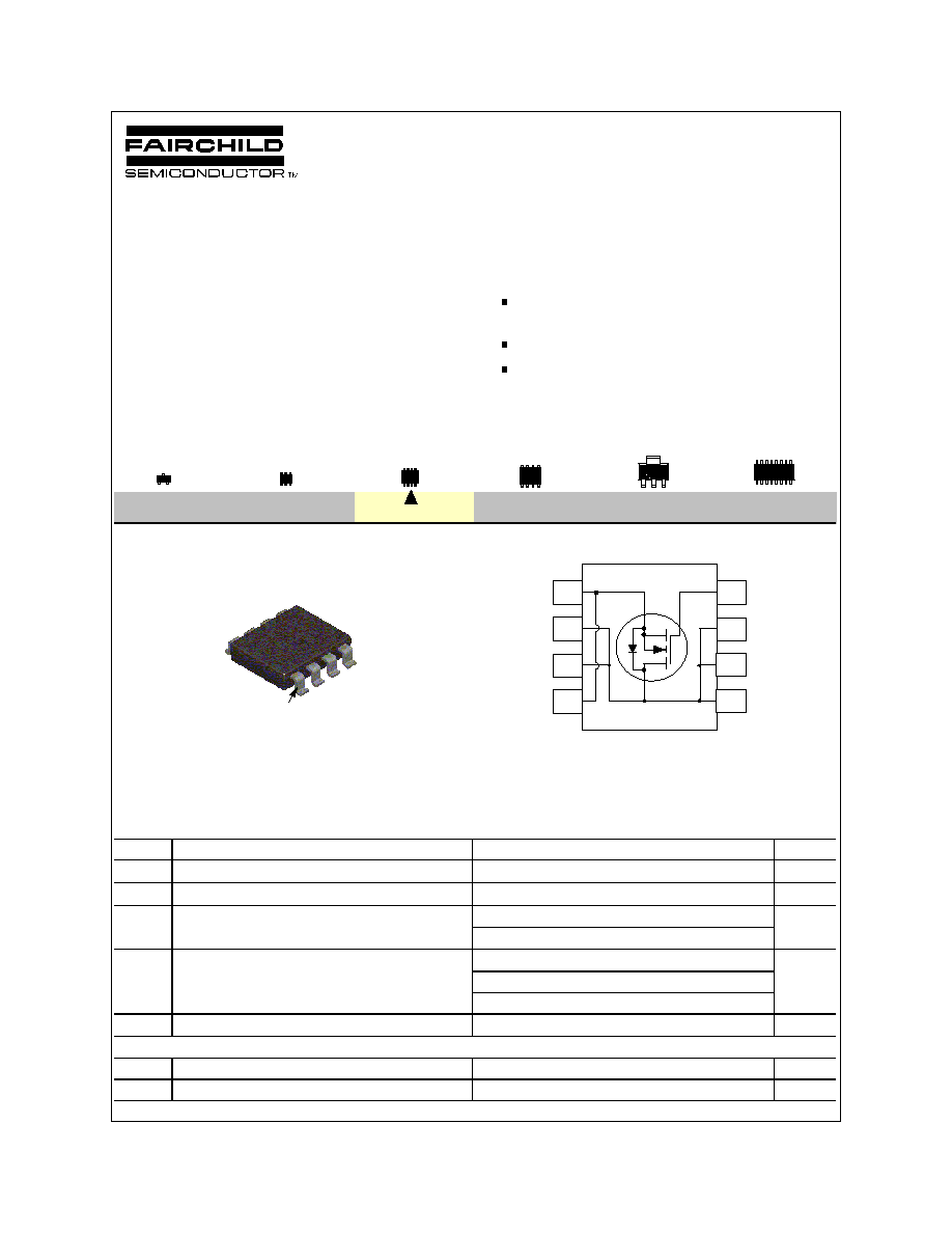
SOT-23
SuperSOT
TM
-8
SOIC-16
SO-8
SOT-223
SuperSOT
TM
-6
D
S
D
D
S
D
D
G
SuperSOT -8
TM
pin
1
4410
1
5
6
7
8
4
3
2
© 1998 Fairchild Semiconductor Corporation

Electrical Characteristics
(T
A
= 25
O
C unless otherwise noted )
Symbol
Parameter
Conditions
Min
Typ
Max
Units
OFF CHARACTERISTICS
BV
DSS
Drain-Source Breakdown Voltage
V
GS
= 0 V, I
D
= 250 µA
30
V
BV
DSS
/
T
J
Breakdown Voltage Temp. Coefficient
I
D
= 250 µA, Referenced to 25
o
C
35
mV/
o
C
I
DSS
Zero Gate Voltage Drain Current
V
DS
= 24 V, V
GS
= 0 V
1
µA
T
J
= 55∞C
25
µA
I
GSS
Gate - Body Leakage Current
V
GS
= 20 V, V
DS
= 0 V
100
nA
I
GSS
Gate - Body Leakage, Reverse
V
GS
= -20 V, V
DS
= 0 V
-100
nA
ON CHARACTERISTICS
(Note 2)
V
GS(th)
Gate Threshold Voltage
V
DS
= V
GS
, I
D
= 250 µA
1
1.5
2
V
V
GS(th)
/
T
J
Gate Threshold Voltage Temp.Coefficient
I
D
= 250 µA, Referenced to 25
o
C
-4.4
mV/
o
C
R
DS(ON)
Static Drain-Source On-Resistance
V
GS
= 10 V, I
D
= 9.3 A
0.011
0.013
T
J
=125∞C
0.017
0.02
V
GS
= 4.5 V, I
D
= 5 A
0.016
0.02
I
D(ON)
On-State Drain Current
V
GS
= 10 V, V
DS
= 5 V
20
A
g
FS
Forward Transconductance
V
DS
= 10 V, I
D
= 9.3 A
25
S
DYNAMIC CHARACTERISTICS
C
iss
Input Capacitance
V
DS
= 15 V, V
GS
= 0 V,
f = 1.0 MHz
1170
pF
C
oss
Output Capacitance
627
pF
C
rss
Reverse Transfer Capacitance
180
pF
SWITCHING CHARACTERISTICS
(Note 2)
t
D(on)
Turn - On Delay Time
V
DD
= 25 V, I
D
= 1 A,
V
GS
= 10 V, R
GEN
= 6
12
22
ns
t
r
Turn - On Rise Time
11
20
ns
t
D(off)
Turn - Off Delay Time
41
66
ns
t
f
Turn - Off Fall Time
34
55
ns
Q
g
Total Gate Charge
V
DS
= 15 V, I
D
= 9.3 A,
V
GS
= 10 V
36
50
nC
Q
gs
Gate-Source Charge
4.5
nC
Q
gd
Gate-Drain Charge
10
nC
DRAIN-SOURCE DIODE CHARACTERISTICS AND MAXIMUM RATINGS
I
S
Maximum Continuous Drain-Source Diode Forward Current
1.5
A
V
SD
Drain-Source Diode Forward Voltage
V
GS
= 0 V, I
S
= 1.5 A
(Note 2)
0.72
1.2
V
Notes:
1. R
JA
is the sum of the junction-to-case and case-to-ambient thermal resistance where the case thermal reference is defined as the solder mounting surface of the drain pins. R
JC
is guaranteed by
design while R
CA
is determined by the user's board design. R
JA
shown below for single device operation on FR-4 board in still air.
Scale 1 : 1 on letter size paper
2. Pulse Test: Pulse Width < 300µs, Duty Cycle < 2.0%.
FDR4410 Rev.C
b. 125
O
C/W on a 0.026 in
2
of pad
of 2oz copper.
a. 70
O
C/W on a 1 in
2
pad of 2oz
copper.
c. 135
O
C/W on a 0.005 in
2
of pad
of 2oz copper.
FDR4410 Rev.C
0
0.5
1
1.5
2
2.5
3
0
10
20
30
40
50
V , DRAIN-SOURCE VOLTAGE (V)
I , DRAIN-SOURCE CURRENT (A)
V = 10V
GS
DS
D
6.0
4.5
3.5
4.0
3.0
5.0
0
10
20
30
40
50
0.5
1
1.5
2
2.5
3
I , DRAIN CURRENT (A)
DRAIN-SOURCE ON-RESISTANCE
V = 3.5V
GS
D
R , NORMALIZED
DS(ON)
10
4.5
5.0
4.0
6.0
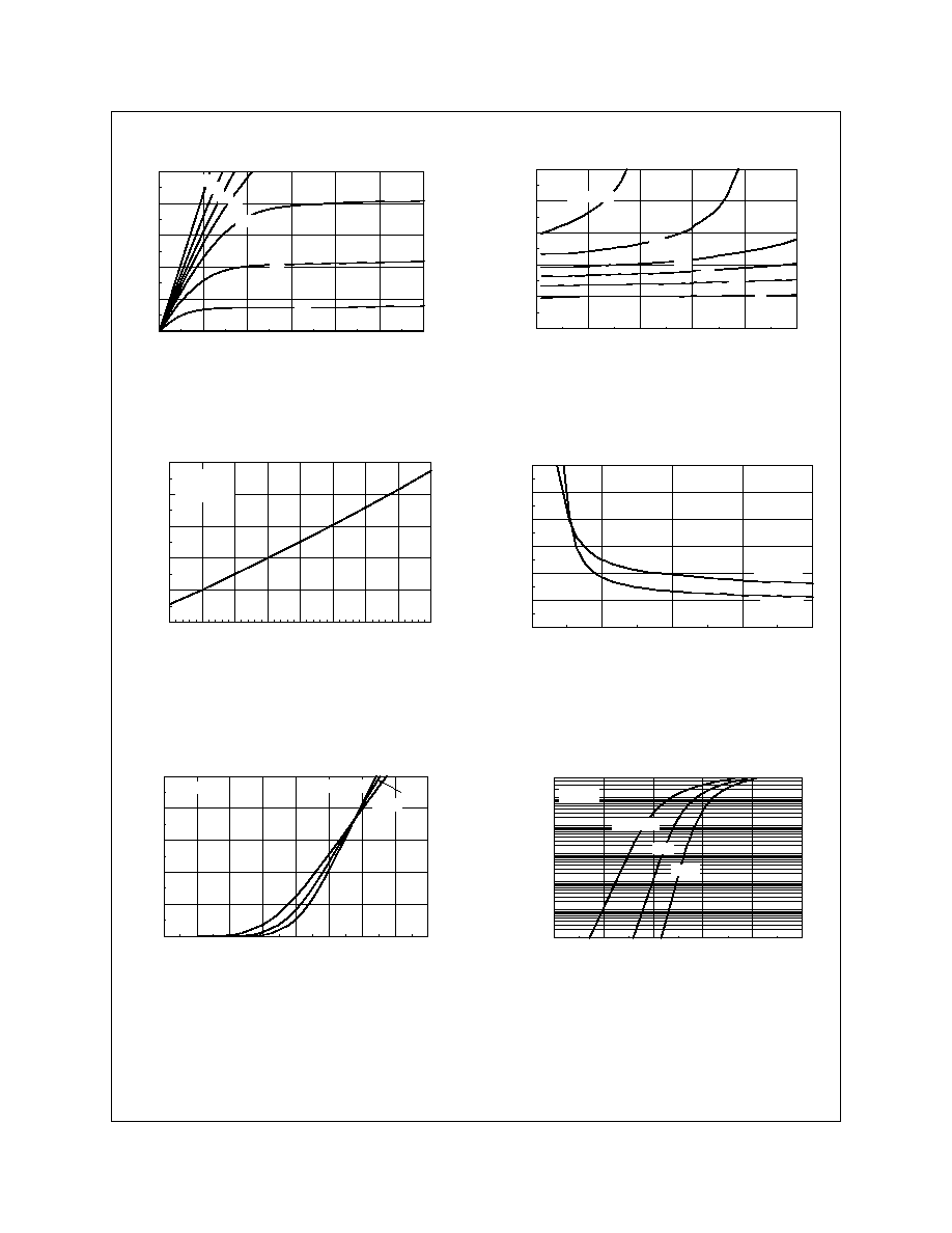
Typical Electrical Characteristics
Figure 1. On-Region Characteristics.
Figure 2. On-Resistance Variation with
Drain Current and Gate Voltage.
-50
-25
0
25
50
75
100
125
150
0.6
0.8
1
1.2
1.4
1.6
T , JUNCTION TEMPERATURE (∞C)
DRAIN-SOURCE ON-RESISTANCE
J
R , NORMALIZED
DS(ON)
V =10V
GS
I =9.3A
D
Figure 3. On-Resistance Variation
with Temperature.
1
1.5
2
2.5
3
3.5
4
4.5
5
0
10
20
30
40
50
V , GATE TO SOURCE VOLTAGE (V)
I , DRAIN CURRENT (A)
V = 10V
DS
GS
D
T = -55∞C
J
125∞C
25∞C
Figure 5. Transfer Characteristics.
0
0.3
0.6
0.9
1.2
1.5
0.0001
0.001
0.01
0.1
1
10
50
V , BODY DIODE FORWARD VOLTAGE (V)
I , REVERSE DRAIN CURRENT (A)
T = 125∞C
J
25∞C
-55∞C
V = 0V
GS
SD
S
2
4
6
8
10
0
0.01
0.02
0.03
0.04
0.05
0.06
V , GATE TO SOURCE VOLTAGE (V)
I = 5A
D
GS
R , ON-RESISTANCE (OHM)
DS(ON)
T = 25∞C
A
T = 125∞C
A
Figure 4. On-Resistance Variation with
Gate-to-Source Voltage.
Figure 6. Body Diode Forward Voltage
Variation with Source Current
and Temperature.
FDR4410 Rev.C
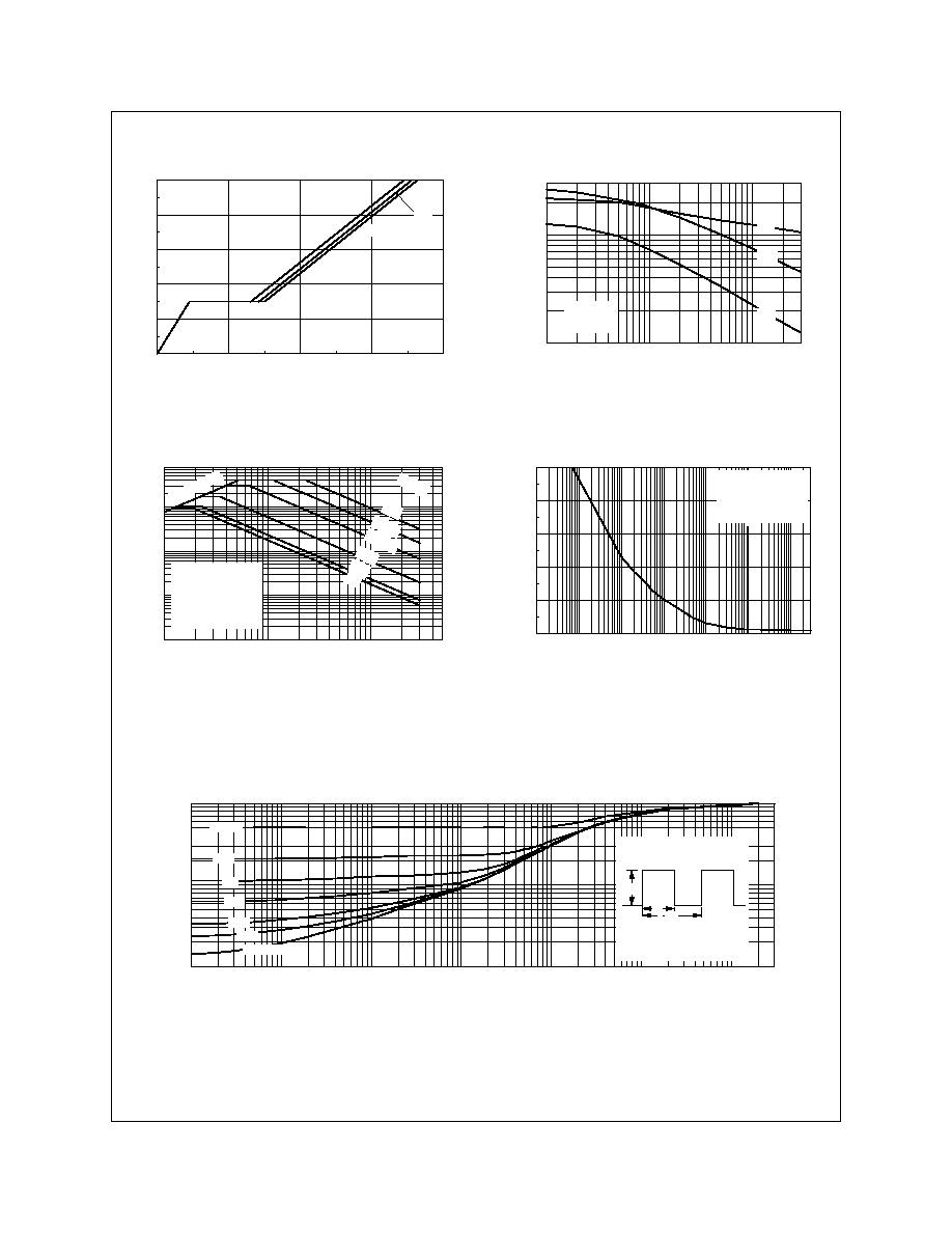
Typical Electrical Characteristics
(continued)
Figure 9. Maximum Safe Operating Area.
0
10
20
30
40
0
2
4
6
8
10
Q , GATE CHARGE (nC)
V , GATE-SOURCE VOLTAGE (V)
V =10V
DS
g
GS
20V
I = 9.3A
D
15V
Figure 7. Gate Charge Characteristics.
0.1
0.2
0.5
1
3
5
10
30
50
0.01
0.03
0.1
0.5
1
5
20
80
V , DRAIN-SOURCE VOLTAGE (V)
I , DRAIN CURRENT (A)
RDS(ON) LIMIT
D
A
DC
DS
1s
100ms
10ms
1ms
10s
V = 10V
SINGLE PULSE
R = See Note 1c
T = 25∞C
JA
GS
A
100µs
Figure 10. Single Pulse Maximum Power
Dissipation.
0.0001
0.001
0.01
0.1
1
10
100
300
0.01
0.02
0.03
0.05
0.1
0.2
0.3
0.5
1
t , TIME (sec)
TRANSIENT THERMAL RESISTANCE
1
Single Pulse
D = 0.5
0.1
0.05
0.02
0.01
0.2
Duty Cycle, D = t / t
1
2
R (t) = r(t) * R
R = See Note 1c
JA
JA
JA
T - T = P * R (t)
JA
A
J
P(pk)
t
1
t
2
r(t), NORMALIZED EFFECTIVE
Figure 11. Transient Thermal Response Curve
.
Thermal characterization performed using the conditions described in note 1c.
Transient thermalresponse will change depending on the circuit board design.
0.1
0.2
0.5
1
2
5
10
20 30
100
200
300
500
1000
2000
3000
V , DRAIN TO SOURCE VOLTAGE (V)
CAPACITANCE (pF)
DS
C
iss
f = 1 MHz
V = 0 V
GS
C
oss
C
rss
Figure 8. Capacitance Characteristics.
0.0001
0.001
0.01
0.1
1
10
100 300
0
10
20
30
40
50
SINGLE PULSE TIME (SEC)
POWER (W)
SINGLE PULSE
R =See Note 1c
T = 25∞C
JA
A