 | ÐлекÑÑоннÑй компоненÑ: FDS4070N3 | СкаÑаÑÑ:  PDF PDF  ZIP ZIP |
Äîêóìåíòàöèÿ è îïèñàíèÿ www.docs.chipfind.ru
May 2003
2002 Fairchild Semiconductor Corporation
FDS4070N3 Rev B1 (W)
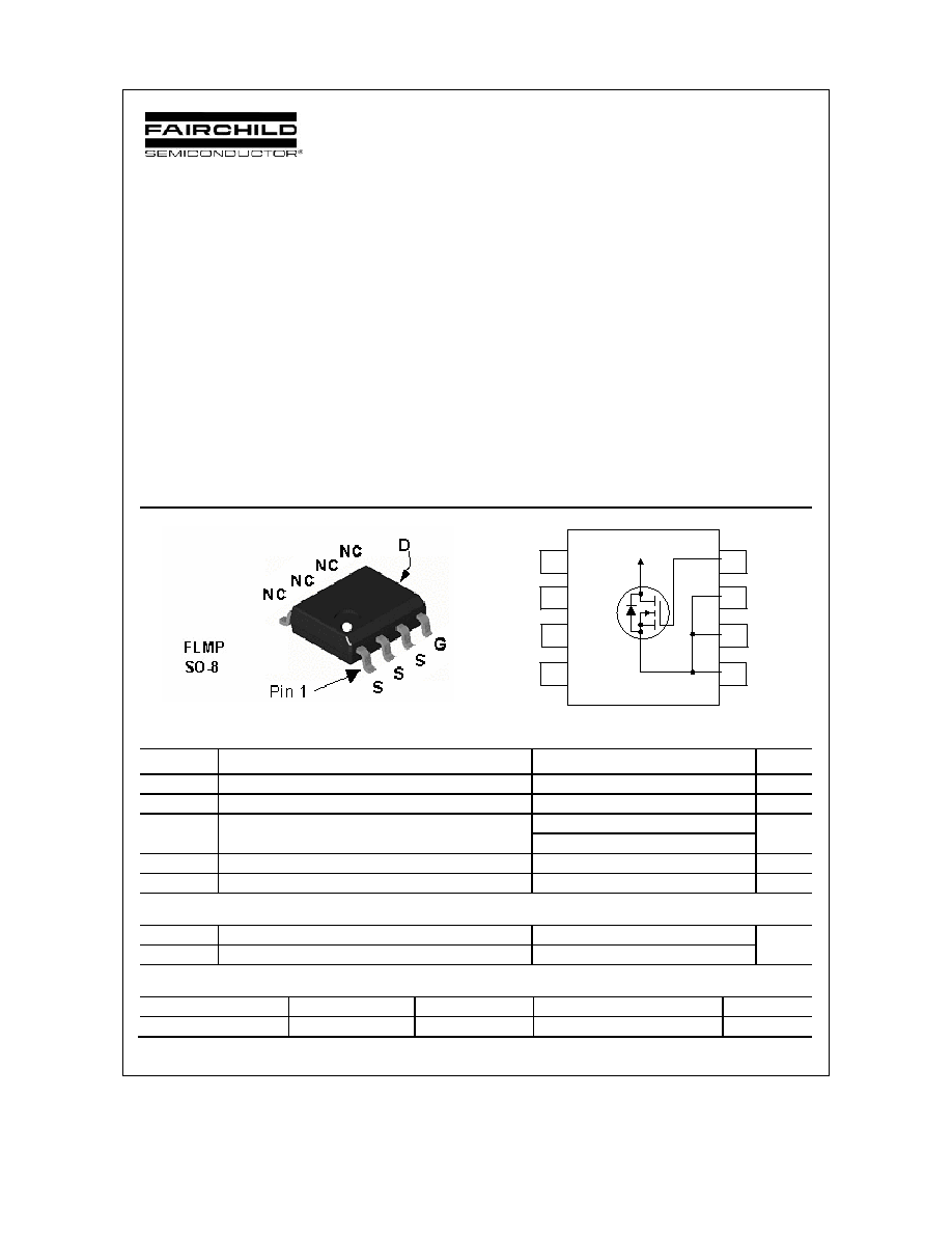
FDS4070N3
40V N-Channel PowerTrench
MOSFET
General Description
This N-Channel MOSFET has been designed
specifically to improve the overall efficiency of DC/DC
converters using either synchronous or conventional
switching PWM controllers. It has been optimized for
"low side" synchronous rectifier operation, providing an
extremely low R
DS(ON)
in a small package.
Applications
· Synchronous rectifier
· DC/DC converter
Features
· 15.3 A, 40 V. R
DS(ON)
= 7.5 m
@ V
GS
= 10 V
· High performance trench technology for extremely
low R
DS(ON)
· High power and current handling capability
· Fast switching, low gate charge
· FLMP SO-8 package: Enhanced thermal
performance in industry-standard package size
4
5
3
6
2
7
1
8
Bottom-side
Drain Contact
Absolute Maximum Ratings
T
A
=25
o
C unless otherwise noted
Symbol Parameter
Ratings
Units
V
DSS
Drain-Source Voltage
40
V
V
GSS
Gate-Source
Voltage
± 20
V
I
D
Drain Current Continuous
(Note 1a)
15.3 A
Pulsed
60
P
D
Maximum Power Dissipation
(Note 1a)
3.0 W
T
J
, T
STG
Operating and Storage Junction Temperature Range
55 to +150
°C
Thermal Characteristics
R
JA
Thermal Resistance, Junction-to-Ambient
(Note 1a)
40
°C/W
R
JC
Thermal Resistance, Junction-to-Case
(Note 1)
0.5
Package Marking and Ordering Information
Device Marking
Device
Reel Size
Tape width
Quantity
FDS4070N3
FDS4070N3
13''
12mm
2500 units
FDS4070N3
FDS4070N3 Rev B1 (W)
Electrical Characteristics
T
A
= 25°C unless otherwise noted
Symbol Parameter
Test
Conditions
Min Typ
Max
Units
Drain-Source Avalanche Ratings
(Note 2)
E
AS
Drain-Source Avalanche Energy
Single Pulse, V
DD
=40V, I
D
=15.3A
310
mJ
I
AS
Drain-Source Avalanche Current
15.3
A
Off Characteristics
BV
DSS
DrainSource Breakdown Voltage
V
GS
= 0 V,
I
D
= 250
µA
40 V
BV
DSS
T
J
Breakdown Voltage Temperature
Coefficient
I
D
= 250
µA, Referenced to 25°C
42 mV/°C
I
DSS
Zero Gate Voltage Drain Current
V
DS
= 32 V, V
GS
= 0 V
1
µA
I
GSSF
GateBody Leakage, Forward
V
GS
= 20 V, V
DS
= 0 V
100
nA
I
GSSR
GateBody Leakage, Reverse
V
GS
= 20 V, V
DS
= 0 V
100
nA
On Characteristics
(Note 2)
V
GS(th)
Gate Threshold Voltage
V
DS
= V
GS
,
I
D
= 250
µA
2 3.9 5 V
V
GS(th)
T
J
Gate Threshold Voltage
Temperature Coefficient
I
D
= 250
µA, Referenced to 25 °C
8
mV/
°C
R
DS(on)
Static DrainSource
OnResistance
V
GS
= 10 V, I
D
= 15.3 A
V
GS
= 10 V, I
D
=15.3A, T
J
=125
°C
5.5
8
7.5
12
m
I
D(on)
OnState Drain Current
V
GS
= 10 V, V
DS
= 5 V
30
A
g
FS
Forward
Transconductance V
DS
= 10 V, I
D
= 15.3 A
52
S
Dynamic Characteristics
C
iss
Input
Capacitance
2819
pF
C
oss
Output
Capacitance
600
pF
C
rss
Reverse Transfer Capacitance
V
DS
= 20 V, V
GS
= 0 V,
f = 1.0 MHz
291 pF
Switching Characteristics
(Note
2)
t
d(on)
TurnOn
Delay
Time
16
29
ns
t
r
TurnOn Rise Time
12
22
ns
t
d(off)
TurnOff Delay Time
41
66
ns
t
f
TurnOff
Fall
Time
V
DD
= 20 V, I
D
= 1 A,
V
GS
= 10 V, R
GEN
= 6
29 46 ns
Q
g
Total Gate Charge
47
67
nC
Q
gs
GateSource
Charge
15
nC
Q
gd
GateDrain
Charge
V
DS
= 20 V, I
D
= 15.3 A,
V
GS
= 10 V
14 nC
FDS4070N3
FDS4070N3 Rev B1 (W)
Electrical Characteristics
T
A
= 25°C unless otherwise noted
Symbol Parameter
Test
Conditions
Min Typ
Max
Units
DrainSource Diode Characteristics and Maximum Ratings
I
S
Maximum Continuous DrainSource Diode Forward Current
2.5
A
V
SD
DrainSource Diode Forward
Voltage
V
GS
= 0 V,
I
S
= 2.5 A
(Note 2)
0.7
1.2 V
t
rr
Diode Reverse Recovery Time
32
nS
Q
rr
Diode Reverse Recovery Charge
I
F
= 15.3 A,
d
iF
/d
t
= 100 A/µs
39 nC
Notes:
1. R
JA
is the sum of the junction-to-case and case-to-ambient thermal resistance where the case thermal reference is defined as the solder mounting surface of
the drain pins. R
JC
is guaranteed by design while R
CA
is determined by the user's board design.
a) 40°C/W
when
mounted on a 1in
2
pad
of 2 oz copper
b)
85°C/W when mounted on
a minimum pad of 2 oz
copper
Scale 1 : 1 on letter size pape
2. Pulse Test: Pulse Width < 300
µs, Duty Cycle < 2.0
FDS4070N3
FDS4070N3 Rev B1 (W)
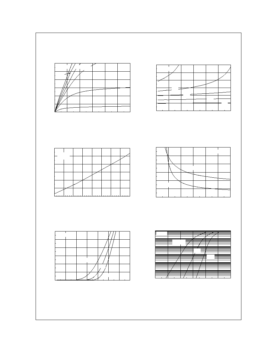
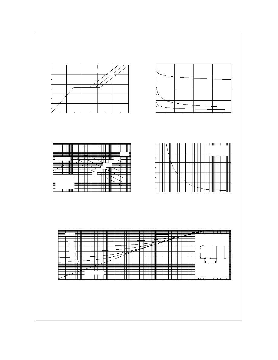
Typical Characteristics
0
10
20
30
40
50
60
0
0.25
0.5
0.75
1
1.25
1.5
V
DS
, DRAIN-SOURCE VOLTAGE (V)
I
D
,
DRAI
N CURRENT (
A
)
5.5V
5.0V
V
GS
= 10V
4.5V
6.0V
7.0V
0.6
1
1.4
1.8
2.2
2.6
3
0
10
20
30
40
50
60
I
D
, DRAIN CURRENT (A)
R
DS(O
N)
,
NORMALI
Z
ED
DRAI
N-
SOURCE ON-
R
ESI
STANCE
V
GS
= 5.0V
7.0V
6.0V
10V
5.5V
Figure 1. On-Region Characteristics.
Figure 2. On-Resistance Variation with
Drain Current and Gate Voltage.
0.6
0.8
1
1.2
1.4
1.6
1.8
-50
-25
0
25
50
75
100
125
150
T
J
, JUNCTION TEMPERATURE (
o
C)
R
DS
(
O
N)
, NORMALIZED
DRAIN-SOURCE ON-RESISTANCE
I
D
= 15.3A
V
GS
= 10V
0.003
0.005
0.007
0.009
0.011
0.013
0.015
4
5
6
7
8
9
10
V
GS
, GATE TO SOURCE VOLTAGE (V)
R
DS(ON)
,
O
N
-
R
ESI
STANCE (
O
HM
)
I
D
= 7.7A
T
A
= 125
o
C
T
A
= 25
o
C
Figure 3. On-Resistance Variation
withTemperature.
Figure 4. On-Resistance Variation with
Gate-to-Source Voltage.
0
10
20
30
40
50
60
2.5
3
3.5
4
4.5
5
5.5
6
V
GS
, GATE TO SOURCE VOLTAGE (V)
I
D
,
DRAI
N CURRENT (A)
T
A
=125
o
C
25
o
C
-55
o
C
V
DS
= 5V
0.0001
0.001
0.01
0.1
1
10
100
0
0.2
0.4
0.6
0.8
1
1.2
V
SD
, BODY DIODE FORWARD VOLTAGE (V)
I
S
, REVERSE DRAIN CURRENT (A)
T
A
= 125
o
C
25
o
C
-55
o
C
V
GS
= 0V
Figure 5. Transfer Characteristics.
Figure 6. Body Diode Forward Voltage Variation
with Source Current and Temperature.
FDS4070N3
FDS4070N3 Rev B1 (W)
Typical Characteristics
0
1000
2000
3000
4000
0
10
20
30
40
V
DS
, DRAIN TO SOURCE VOLTAGE (V)
CAPACITANCE (pF)
C
ISS
C
RSS
C
OSS
f = 1MHz
V
GS
= 0 V
Figure 7. Gate Charge Characteristics.
Figure 8. Capacitance Characteristics.
0.01
0.1
1
10
100
1000
0.01
0.1
1
10
100
V
DS
, DRAIN-SOURCE VOLTAGE (V)
I
D
, DRAIN CURRENT (A)
DC
1s
100ms
R
DS(ON)
LIMIT
V
GS
= 10V
SINGLE PULSE
R
JA
= 85
o
C/W
T
A
= 25
o
C
10ms
1ms
100µs
10s
0
10
20
30
40
50
0.01
0.1
1
10
100
1000
t
1
, TIME (sec)
P(
pk)
,
PEAK TRANSI
E
NT PO
W
E
R (
W
)
SINGLE PULSE
R
JA
= 85°C/W
T
A
= 25°C
Figure 9. Maximum Safe Operating Area.
Figure 10. Single Pulse Maximum
Power Dissipation.
0.001
0.01
0.1
1
0.0001
0.001
0.01
0.1
1
10
100
1000
t
1
, TIME (sec)
r(t), NORMALIZED EFFECTIVE TRANSIENT
THERMAL RESISTANCE
R
JA
(t) = r(t) * R
JA
R
JA
= 85 °C/W
T
J
- T
A
= P * R
JA
(t)
Duty Cycle, D = t
1
/ t
2
P(pk)
t
1
t
2
SINGLE PULSE
0.01
0.02
0.05
0.1
0.2
D = 0.5
Figure 11. Transient Thermal Response Curve.
Thermal characterization performed using the conditions described in Note 1b.
Transient thermal response will change depending on the circuit board design.
FDS4070N3
0
2
4
6
8
10
0
10
20
30
40
50
Q
g
, GATE CHARGE (nC)
V
GS
, GA
TE-
S
OUR
C
E
V
O
LTA
GE
(
V
)
I
D
= 15.3
V
DS
= 10V
20V
30V
FDS4070N3 Rev B1 (W)
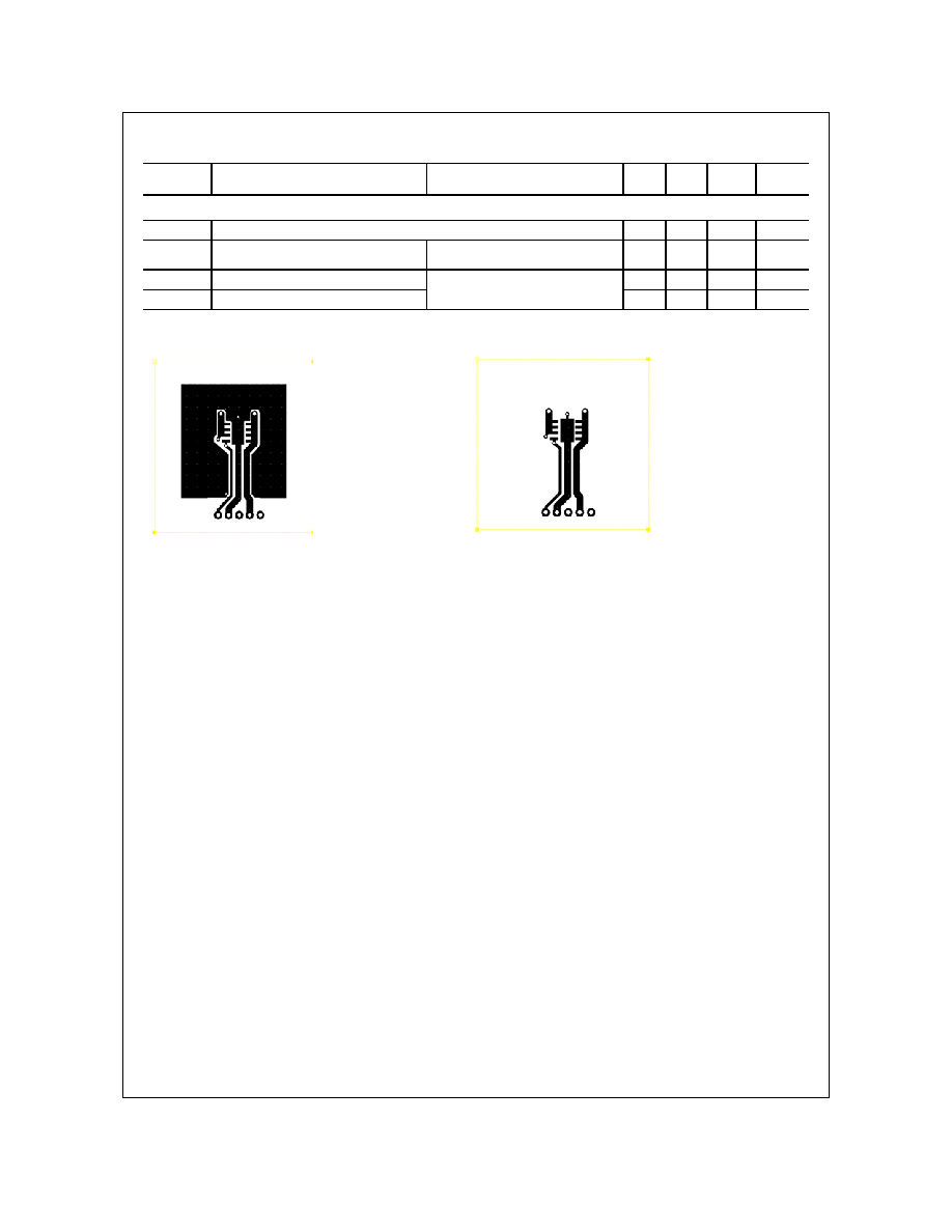
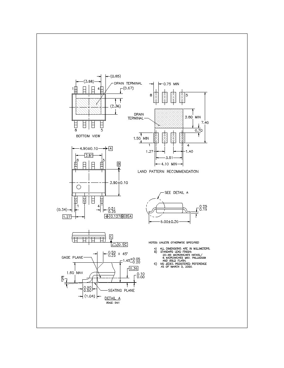
Dimensional Outline and Pad Layout
FDS4070N3

DISCLAIMER
FAIRCHILD SEMICONDUCTOR RESERVES THE RIGHT TO MAKE CHANGES WITHOUT FURTHER
NOTICE TO ANY PRODUCTS HEREIN TO IMPROVE RELIABILITY, FUNCTION OR DESIGN. FAIRCHILD
DOES NOT ASSUME ANY LIABILITY ARISING OUT OF THE APPLICATION OR USE OF ANY PRODUCT
OR CIRCUIT DESCRIBED HEREIN; NEITHER DOES IT CONVEY ANY LICENSE UNDER ITS PATENT
RIGHTS, NOR THE RIGHTS OF OTHERS.
TRADEMARKS
The following are registered and unregistered trademarks Fairchild Semiconductor owns or is authorized to use and is
not intended to be an exhaustive list of all such trademarks.
LIFE SUPPORT POLICY
FAIRCHILDS PRODUCTS ARE NOT AUTHORIZED FOR USE AS CRITICAL COMPONENTS IN LIFE SUPPORT
DEVICES OR SYSTEMS WITHOUT THE EXPRESS WRITTEN APPROVAL OF FAIRCHILD SEMICONDUCTOR CORPORATION.
As used herein:
1. Life support devices or systems are devices or
systems which, (a) are intended for surgical implant into
the body, or (b) support or sustain life, or (c) whose
failure to perform when properly used in accordance
with instructions for use provided in the labeling, can be
reasonably expected to result in significant injury to the
user.
2. A critical component is any component of a life
support device or system whose failure to perform can
be reasonably expected to cause the failure of the life
support device or system, or to affect its safety or
effectiveness.
PRODUCT STATUS DEFINITIONS
Definition of Terms
Datasheet Identification
Product Status
Definition
Advance Information
Preliminary
No Identification Needed
Obsolete
This datasheet contains the design specifications for
product development. Specifications may change in
any manner without notice.
This datasheet contains preliminary data, and
supplementary data will be published at a later date.
Fairchild Semiconductor reserves the right to make
changes at any time without notice in order to improve
design.
This datasheet contains final specifications. Fairchild
Semiconductor reserves the right to make changes at
any time without notice in order to improve design.
This datasheet contains specifications on a product
that has been discontinued by Fairchild semiconductor.
The datasheet is printed for reference information only.
Formative or
In Design
First Production
Full Production
Not In Production
ImpliedDisconnect
ISOPLANAR
LittleFET
MicroFET
MicroPak
MICROWIRE
MSX
MSXPro
OCX
OCXPro
OPTOLOGIC
â
OPTOPLANAR
FACT
FACT Quiet Series
FAST
â
FASTr
FRFET
GlobalOptoisolator
GTO
HiSeC
I
2
C
Rev. I2
ACEx
ActiveArray
Bottomless
CoolFET
CROSSVOLT
DOME
EcoSPARK
E
2
CMOS
TM
EnSigna
TM
PACMAN
POP
Power247
PowerTrench
â
QFET
QS
QT Optoelectronics
Quiet Series
RapidConfigure
RapidConnect
SILENT SWITCHER
â
SMART START
SPM
Stealth
SuperSOT-3
SuperSOT-6
SuperSOT-8
SyncFET
TinyLogic
â
TruTranslation
UHC
UltraFET
â
VCX
Across the board. Around the world.
The Power Franchise
Programmable Active Droop