 | –≠–ª–µ–∫—Ç—Ä–æ–Ω–Ω—ã–π –∫–æ–º–ø–æ–Ω–µ–Ω—Ç: FDS4072N3 | –°–∫–∞—á–∞—Ç—å:  PDF PDF  ZIP ZIP |
May 2003
2002 Fairchild Semiconductor Corporation
FDS4072N3 Rev B1 (W)
FDS4072N3
40V N-Channel PowerTrench
MOSFET
General Description
This N-Channel MOSFET has been designed
specifically to improve the overall efficiency of DC/DC
converters using either synchronous or conventional
switching PWM controllers. It has been optimized for
"low side" synchronous rectifier operation, providing an
extremely low R
DS(ON)
in a small package.
Applications
∑ Synchronous rectifier
∑ DC/DC converter
Features
∑ 12.4 A, 40 V R
DS(ON)
= 12 m
@ V
GS
= 4.5 V
R
DS(ON)
= 10 m
@ V
GS
= 10 V
∑ High performance trench technology for extremely
low R
DS(ON)
∑ High power and current handling capability
∑ Fast switching
∑ FLMP SO-8 package: Enhanced thermal
performance in industry-standard package size
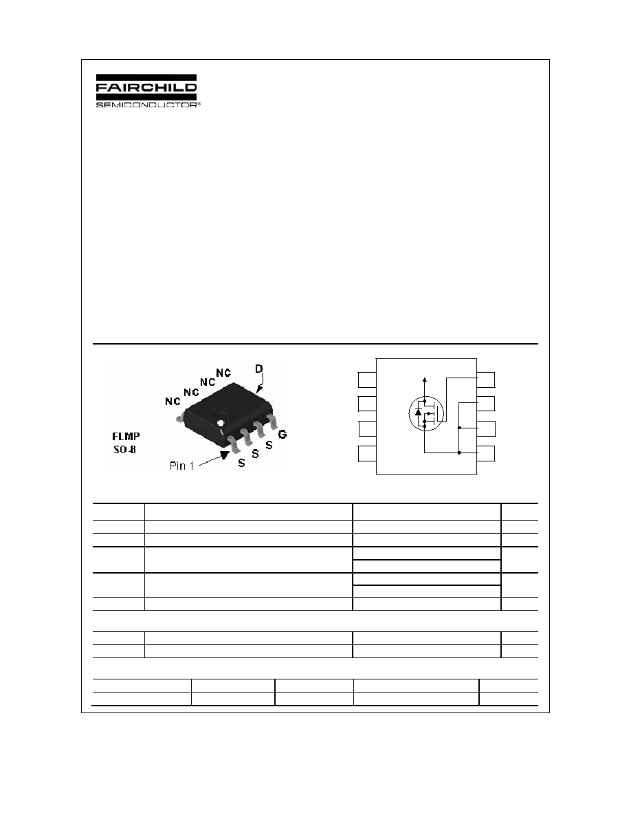
4
5
3
6
2
7
1
8
Bottom-side
Drain Contact
Absolute Maximum Ratings
T
A
=25
o
C unless otherwise noted
Symbol Parameter
Ratings
Units
V
DSS
Drain-Source Voltage
40
V
V
GSS
Gate-Source
Voltage
± 12
V
I
D
Drain Current ≠ Continuous
(Note 1a)
12.4 A
≠
Pulsed
60
Power Dissipation
(Note 1a)
3.0
P
D
(Note
1b)
1.5
W
T
J
, T
STG
Operating and Storage Junction Temperature Range
≠55 to +150
∞C
Thermal Characteristics
R
JA
Thermal Resistance, Junction-to-Ambient
(Note 1a)
40
∞C/W
R
JC
Thermal Resistance, Junction-to-Case
0.5
∞C/W
Package Marking and Ordering Information
Device Marking
Device
Reel Size
Tape width
Quantity
FDS4072N3
FDS4072N3
13''
12mm
2500 units
FDS4072N3

FDS4072N3 Rev B1 (W)
Electrical Characteristics
T
A
= 25∞C unless otherwise noted
Symbol Parameter
Test
Conditions
Min
Typ
Max
Units
Drain-Source Avalanche Ratings
(Note 2)
E
AS
Drain-Source Avalanche Energy
Single Pulse, V
DD
= 20V, I
D
=12.4 A
200
mJ
I
AS
Drain-Source Avalanche Current
12.4
A
Off Characteristics
BV
DSS
Drain≠Source Breakdown Voltage V
GS
= 0 V,
I
D
= 250
µA
40 V
BV
DSS
T
J
Breakdown Voltage Temperature
Coefficient
I
D
= 250
µA, Referenced to 25∞C
38
mV/
∞C
I
DSS
Zero Gate Voltage Drain Current
V
DS
= 32 V,
V
GS
= 0 V
1
µA
I
GSSF
Gate≠Body Leakage, Forward
V
GS
= 12 V,
V
DS
= 0 V
100
nA
I
GSSR
Gate≠Body Leakage, Reverse
V
GS
= ≠12 V , V
DS
= 0 V
≠100
nA
On Characteristics
(Note 2)
V
GS(th)
Gate Threshold Voltage
V
DS
= V
GS
,
I
D
= 250
µA
1 1.3 3 V
V
GS(th)
T
J
Gate Threshold Voltage
Temperature Coefficient
I
D
= 250
µA, Referenced to 25∞C
≠4.5
mV/
∞C
R
DS(on)
Static Drain≠Source
On≠Resistance
V
GS
= 4.5 V, I
D
= 12.4 A
V
GS
= 10 V, I
D
= 13.7 A
V
GS
= 4.5 V, I
D
= 12.4 A,T
J
= 125
∞C
9.7
8.5
14.7
12
10
20
m
I
D(on)
On≠State Drain Current
V
GS
= 5 V,
V
DS
= 5 V
30
A
g
FS
Forward
Transconductance V
DS
= 10 V,
I
D
= 12.4 A
84
S
Dynamic Characteristics
C
iss
Input
Capacitance
4299
pF
C
oss
Output
Capacitance
351
pF
C
rss
Reverse Transfer Capacitance
V
DS
= 20 V,
V
GS
= 0 V,
f = 1.0 MHz
149 pF
Switching Characteristics
(Note 2)
t
d(on)
Turn≠On
Delay
Time
20
36
ns
t
r
Turn≠On Rise Time
12
22
ns
t
d(off)
Turn≠Off Delay Time
52
83
ns
t
f
Turn≠Off
Fall
Time
V
DD
= 20 V,
I
D
= 1 A,
V
GS
= 4.5 V,
R
GEN
= 6
18
32 ns
Q
g
Total Gate Charge
33
46
nC
Q
gs
Gate≠Source
Charge
7.8
nC
Q
gd
Gate≠Drain
Charge
V
DS
= 20 V,
I
D
= 12.4 A,
V
GS
= 4.5 V
8.1 nC
Drain≠Source Diode Characteristics and Maximum Ratings
I
S
Maximum Continuous Drain≠Source Diode Forward Current
2.5
A
V
SD
Drain≠Source Diode Forward
Voltage
V
GS
= 0 V, I
S
= 2.5 A
(Note 2)
0.7
1.2
V
t
rr
Diode Reverse Recovery Time
30
nS
Q
rr
Diode Reverse Recovery Charge
I
F
= 12.4 A,
d
iF
/d
t
= 100 A/µs
90 nC
FDS4072N3
FDS4072N3 Rev B1 (W)
Electrical Characteristics
T
A
= 25∞C unless otherwise noted
Notes:
1. R
JA
is the sum of the junction-to-case and case-to-ambient thermal resistance where the case thermal reference is defined as the solder mounting surface of
the drain pins. R
JC
is guaranteed by design while R
CA
is determined by the user's board design.
a)
40∞C/W when mounted
on a 1in
2
pad of 2 oz
copper
b)
85∞C/W when mounted on
a minimum pad of 2 oz
copper
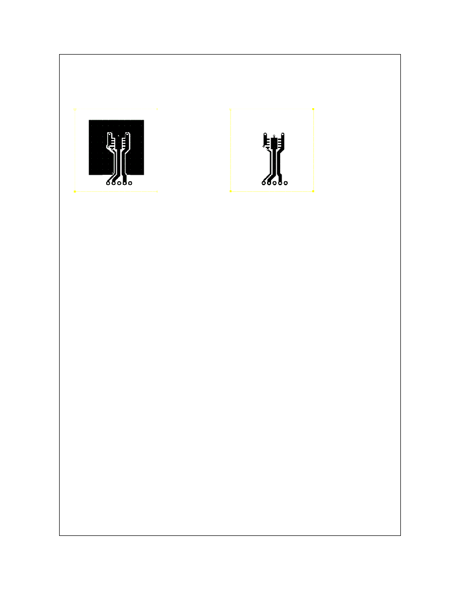
Scale 1 : 1 on letter size paper
2. Pulse Test: Pulse Width < 300
µs, Duty Cycle < 2.0%
FDS4072N3

FDS4072N3 Rev B1 (W)
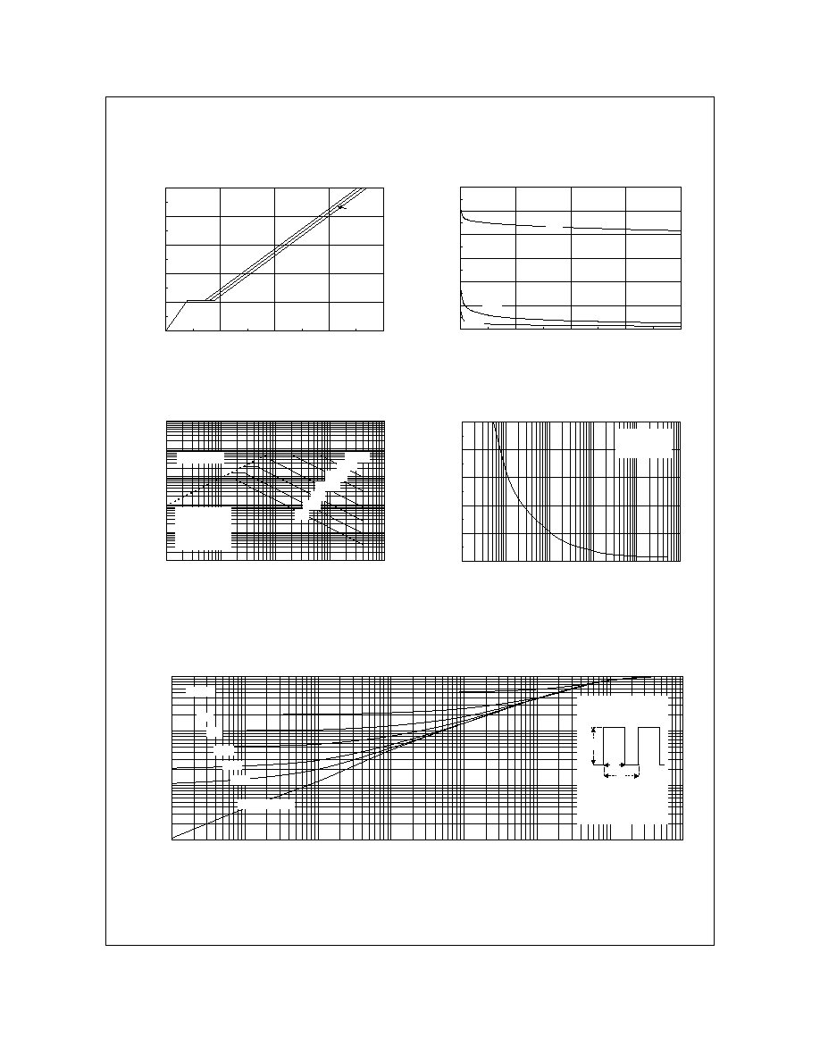
Typical Characteristics
0
20
40
60
80
0
1
2
3
4
V
DS
, DRAIN-SOURCE VOLTAGE (V)
I
D
, DRAIN CURRENT
(
A
)
2.5V
V
GS
=10V
4.5V
3.0V
0.8
1
1.2
1.4
1.6
0
20
40
60
80
I
D
, DRAIN CURRENT (A)
R
DS(O
N)
, NORMALIZED
DRAIN-SOURCE ON-RESISTANCE
V
GS
= 2.5V
3.0V
10V
4.5V
3.5V
Figure 1. On-Region Characteristics.
Figure 2. On-Resistance Variation with
Drain Current and Gate Voltage.
0.4
0.7
1
1.3
1.6
1.9
-50
-25
0
25
50
75
100
125
150
T
J
, JUNCTION TEMPERATURE (
o
C)
R
DS(
O
N)
, NORMALIZED
DRAIN-
SOURCE ON-
R
ESISTANCE
I
D
= 12.4A
V
GS
= 4.5V
0.005
0.01
0.015
0.02
0.025
1
4
7
10
V
GS
, GATE TO SOURCE VOLTAGE (V)
R
DS
(ON)
, ON-RESISTANCE (OHM)
I
D
= 6.2A
T
A
= 125
o
C
T
A
= 25
o
C
Figure 3. On-Resistance Variation
withTemperature.
Figure 4. On-Resistance Variation with
Gate-to-Source Voltage.
0
20
40
60
80
1
1.5
2
2.5
3
V
GS
, GATE TO SOURCE VOLTAGE (V)
I
D
, DRAIN CURRENT (
A
)
T
A
=125
o
C
25
o
C
-55
o
C
V
DS
= 5V
0.0001
0.001
0.01
0.1
1
10
100
0
0.2
0.4
0.6
0.8
1
1.2
V
SD
, BODY DIODE FORWARD VOLTAGE (V)
I
S
, REVERSE DRAIN CURRENT (
A
)
T
A
= 125
o
C
25
o
C
-55
o
C
V
GS
= 0V
Figure 5. Transfer Characteristics.
Figure 6. Body Diode Forward Voltage Variation
with Source Current and Temperature.
FDS4072N3
FDS4072N3 Rev B1 (W)
Typical Characteristics
0
2
4
6
8
10
0
20
40
60
80
Q
g
, GATE CHARGE (nC)
V
GS
, GATE-
S
OURCE VOLTAGE (
V
)
I
D
= 12.4A
V
DS
= 10V
30V
20V
0
1000
2000
3000
4000
5000
6000
0
10
20
30
40
V
DS
, DRAIN TO SOURCE VOLTAGE (V)
CAPACITANCE (
pF)
C
ISS
C
RSS
C
OSS
f = 1MHz
V
GS
= 0 V
Figure 7. Gate Charge Characteristics.
Figure 8. Capacitance Characteristics.
0.01
0.1
1
10
100
1000
0.01
0.1
1
10
100
V
DS
, DRAIN-SOURCE VOLTAGE (V)
I
D
, DRAIN CURRENT (
A
)
DC
1s
100ms
R
DS(ON)
LIMIT
V
GS
= 4.5V
SINGLE PULSE
R
JA
= 85
o
C/W
T
A
= 25
o
C
10ms
1ms
100µs
10s
0
10
20
30
40
50
0.01
0.1
1
10
100
1000
t
1
, TIME (sec)
P(
p
k
)
,
PEAK T
RANSIENT
POWER (
W
)
SINGLE PULSE
R
JA
= 85∞C/W
T
A
= 25∞C
Figure 9. Maximum Safe Operating Area.
Figure 10. Single Pulse Maximum
Power Dissipation.
0.001
0.01
0.1
1
0.0001
0.001
0.01
0.1
1
10
100
1000
t
1
, TIME (sec)
r(t), NO
RM
ALIZED EFFECTIVE TRANSIEN
T
THERM
A
L RESISTANCE
R
JA
(t) = r(t) * R
JA
R
JA
= 85 ∞C/W
T
J
- T
A
= P * R
JA
(t)
Duty Cycle, D = t
1
/ t
2
P(pk)
t
1
t
2
SINGLE PULSE
0.01
0.02
0.05
0.1
0.2
D = 0.5
Figure 11. Transient Thermal Response Curve.
Thermal characterization performed using the conditions described in Note 1b.
Transient thermal response will change depending on the circuit board design.
FDS4072N3