 | ÐлекÑÑоннÑй компоненÑ: FDS6815 | СкаÑаÑÑ:  PDF PDF  ZIP ZIP |
Äîêóìåíòàöèÿ è îïèñàíèÿ www.docs.chipfind.ru
FDS6815
FDS6815 Rev. A
FDS6815
Dual P-Channel 2.5V Specified PowerTrench
TM
MOSFET
1999 Fairchild Semiconductor Corporation
July 1999
ADVANCE INFORMATION
Absolute Maximum Ratings
T
A
=25
o
C unless otherwise noted
Symbol
Parameter
Ratings
Units
V
DSS
Drain-Source Voltage
20
V
V
GSS
Gate-Source Voltage
±
12
V
I
D
Drain Current
- Continuous
(Note 1a)
5.5
A
- Pulsed
50
Power Dissipation for Dual Operation
2.0
Power Dissipation for Single Operation
(Note 1a)
1.6
(Note 1b)
1.0
P
D
(Note 1c)
0.9
W
T
J
, T
stg
Operating and Storage Junction Temperature Range
-55 to +150
°
C
Thermal Characteristics
R
JA
Thermal Resistance, Junction-to-Ambient
(Note 1a)
78
°
C/W
R
JC
Thermal Resistance, Junction-to-Case
(Note 1)
40
°
C/W
Package Marking and Ordering Information
Device Marking
Device
Reel Size
Tape Width
Quantity
FDS6815
FDS6815
13''
12mm
2500 units
General Description
These P-Channel 2.5V specified MOSFETs are produced
using a rugged gate version of Fairchild's advanced
PowerTrench
TM
process. It has been optimized for
power management applications which require a wide
range of gate drive voltages.
Applications
Load switch
Battery protection
Power management
Features
-5.5 A, 20 V. R
DS(ON)
= 0.040
@ V
GS
= 4.5 V
R
DS(ON)
= 0.050
@ V
GS
= 2.5 V
Extended V
GSS
range (
±
12V) for battery applications.
Low gate charge.
Fast switching speed.
High performance trench technology for extremely
low R
DS(ON)
.
High power and current handling capability.
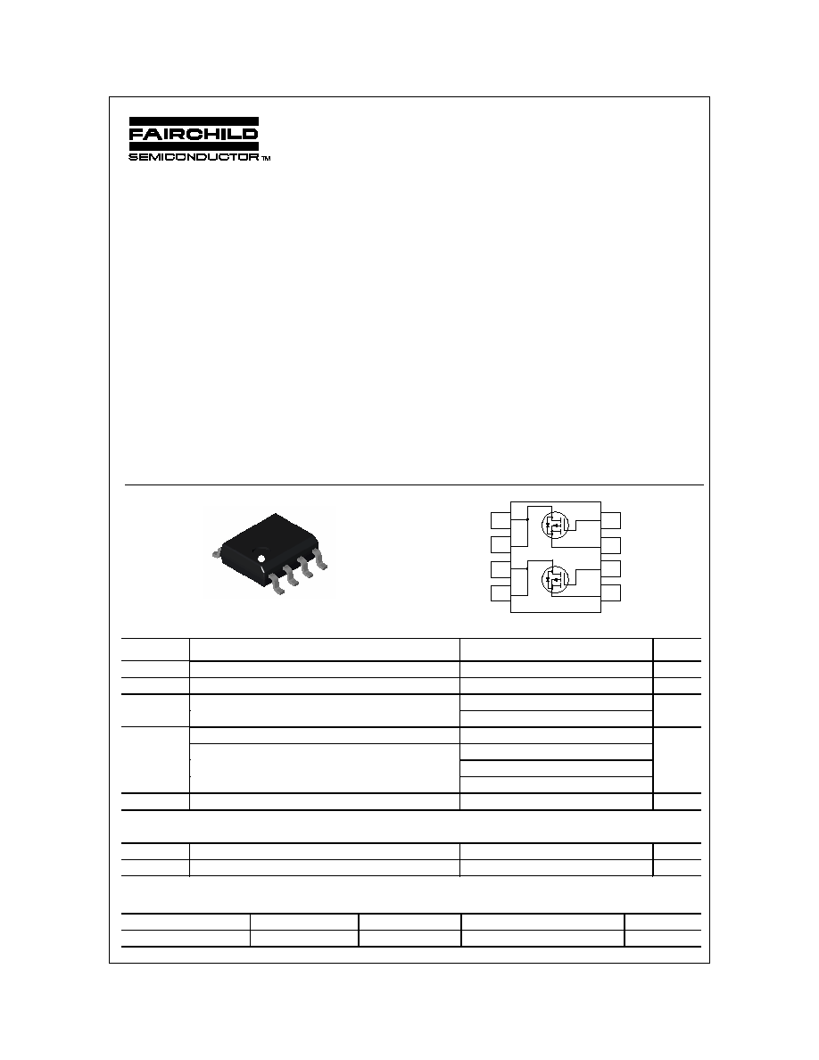
D1
SO-8
D2
D2
D1
S1
S2
G1
G2
1
5
7
8
2
3
4
6
FDS6815
FDS6815 Rev. A
Electrical Characteristics
T
A
=25
o
C unless otherwise noted
Symbol
Parameter
Test Conditions
Min
Typ
Max
Units
OFF CHARACTERISTICS
BV
DSS
Drain-Source Breakdown Voltage
V
GS
= 0 V, I
D
= -250
µ
A
-20
V
I
DSS
Zero Gate Voltage Drain Current
V
DS
= -16 V, V
GS
= 0 V
1
µ
A
I
GSSF
Gate-Body Leakage, Forward
V
GS
= 12 V, V
DS
= 0 V
100
nA
I
GSSR
Gate-Body Leakage, Reverse
V
GS
= -12 V, V
DS
= 0 V
-100
nA
ON CHARACTERISTICS
(Note 2)
V
GS(TH)
Gate Threshold Voltage
V
DS
= V
GS
, I
D
= -250
µ
A
-0.6
-1.5
V
R
DS(ON)
Static Drain-Source
On-Resistance
V
GS
= -4.5 V, I
D
= -5.5 A
V
GS
= -2.5 V, I
D
= -5 A
0.04
0.05
I
D(ON)
On-State Drain Current
V
GS
= -4.5 V, V
DS
= -5.0 V
25
A
DRAIN-SOURCE DIODE CHARACTERISTICS AND MAXIMUM RATINGS
I
S
Maximum Continuous Drain-Source Diode Forward Current
-1.3
A
V
SD
Drain-Source Diode Forward
Voltage
V
GS
= 0 V, I
S
= -1.3 A
(Note 2)
-1.2
V
Notes:
1. R
JA
is the sum of the junction-to-case and case-to-ambient thermal resistance where the case thermal reference is defined as the solder mounting surface of the drain pins.
R
JC
is guaranteed by design while R
JA
is determined by the user's board design. Thermal rating based on independent single device operation.
Scale 1 : 1 on letter size paper
2. Pulse Test: Pulse Width
300
µ
s, Duty Cycle
2.0%
a) 78
°
C/W when
mounted on a 0.5 in
2
pad of 2 oz. copper.
b) 125
°
C/W when
mounted on a 0.02 in
2
pad of 2 oz. copper.
c) 135
°
C/W when
mounted on a minimum pad.
F
852
831N
F
852
831N
F
852
831N
F
852
831N
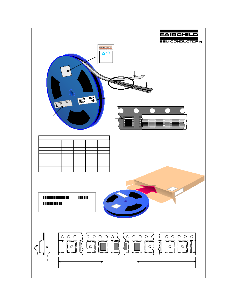
SOIC-8 Unit Orientation
Conductive Embossed
Carrier Tape
F63TNR
Label
ESD Label
Antistatic Cover Tape
SOIC(8lds) Packaging
Configuration: Figure 1.0
Components
Leader Tape
390mm minimum
Trailer Tape
160mm minimum
SOIC(8lds) Tape Leader and Trailer
Configuration: Figure 2.0
Cover Tape
Carrier
Pin 1
Tape
Note/Comments
Bulk
Packaging Option
SOIC (8lds) Packaging Information
Standard
(no flow code)
L86Z
S62Z
Packaging type
Reel Size
TNR
13" Dia
Rail/Tube
-
Bag
-
Qty per Reel/Tube/Bag
2,500
95
200
Box Dimension (mm)
343x64x343
530x130x83
76x102x127
Max qty per Box
5,000
30,000
1,000
D84Z
TNR
7" Dia
500
184x187x47
2,500
Weight per unit (gm)
0.0774
0.0774
0.0774
0.0774
Weight per Reel (kg)
0.6060
-
-
0.1182
N
ELECTROSTATIC
SENSITIVE DEVICES
DO NOT SHIP OR STORE NEAR STRONG ELECTROSTATIC
ELECTROMAGNETIC, MAGNETIC OR RADIOACTIVE FIELDS
TNR DATE
PT NUMBER
PEEL STRENGTH MIN ______________ gms
MAX _____________ gms
LOT: CBVK741B019
FSID: FDS9953A
D/C1: D9842
QTY1:
SPEC REV: QARV:
SPEC:
QTY: 2500
D/C2:
QTY2:
CPN:
(F63TNR)2
F63TNLabel
ESD Label
343mm x 342mm x 64mm
Standard Intermediate box
ESD Label
F63TNR Label sample
F63TNLabel
Customized
Label
SO-8 Tape and Reel Data and Package Dimensions
November 1998, Rev. A
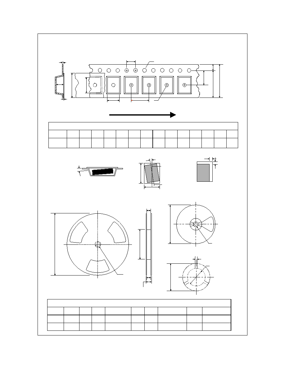
©
1998 Fairchild Semiconductor Corporation
Dimensions are in millimeter
Pkg type
A0
B0
W
D0
D1
E1
E2
F
P1
P0
K0
T
Wc
Tc
SOIC(8lds)
(12mm)
6.50
+/-0.10
5.30
+/-0.10
12.0
+/-0.3
1.55
+/-0.05
1.60
+/-0.10
1.75
+/-0.10
10.25
min
5.50
+/-0.05
8.0
+/-0.1
4.0
+/-0.1
2.1
+/-0.10
0.450
+/-
0.150
9.2
+/-0.3
0.06
+/-0.02
P1
A0
D1
P0
F
W
E1
D0
E2
B0
Tc
Wc
K0
T
Dimensions are in inches and millimeters
Tape Size
Reel
Option
Dim A
Dim B
Dim C
Dim D
Dim N
Dim W1
Dim W2
Dim W3 (LSL-USL)
12mm
7" Dia
7.00
177.8
0.059
1.5
512 +0.020/-0.008
13 +0.5/-0.2
0.795
20.2
5.906
150
0.488 +0.078/-0.000
12.4 +2/0
0.724
18.4
0.469 0.606
11.9 15.4
12mm
13" Dia
13.00
330
0.059
1.5
512 +0.020/-0.008
13 +0.5/-0.2
0.795
20.2
7.00
178
0.488 +0.078/-0.000
12.4 +2/0
0.724
18.4
0.469 0.606
11.9 15.4
See detail AA
Dim A
max
13" Diameter Option
7" Diameter Option
Dim A
Max
See detail AA
W3
W2 max Measured at Hub
W1 Measured at Hub
Dim N
Dim D
min
Dim C
B Min
DETAIL AA
Notes: A0, B0, and K0 dimensions are determined with respect to the EIA/Jedec RS-481
rotational and lateral movement requirements (see sketches A, B, and C).
20 deg maximum component rotation
0.5mm
maximum
0.5mm
maximum
Sketch C (Top View)
Component lateral movement
Typical
component
cavity
center line
20 deg maximum
Typical
component
center line
B0
A0
Sketch B (Top View)
Component Rotation
Sketch A (Side or Front Sectional View)
Component Rotation
User Direction of Feed
SOIC(8lds) Embossed Carrier Tape
Configuration: Figure 3.0
SOIC(8lds) Reel Configuration: Figure 4.0
SO-8 Tape and Reel Data and Package Dimensions, continued
November 1998, Rev. A
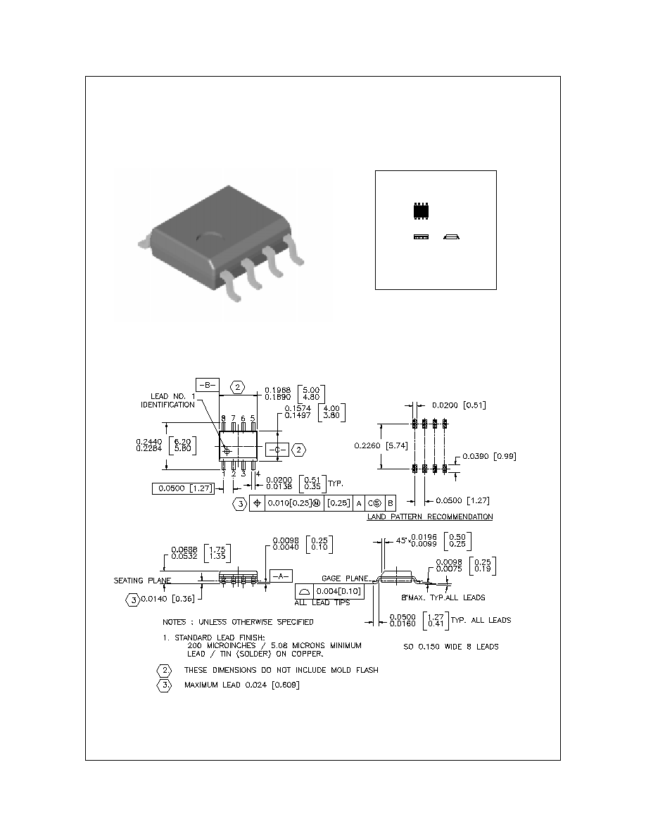
SOIC-8 (FS PKG Code S1)
1 : 1
Scale 1:1 on letter size paper
Dimensions shown below are in:
inches [millimeters]
Part Weight per unit (gram): 0.0774
SO-8 Tape and Reel Data and Package Dimensions, continued
September 1998, Rev. A
9