 | –≠–ª–µ–∫—Ç—Ä–æ–Ω–Ω—ã–π –∫–æ–º–ø–æ–Ω–µ–Ω—Ç: FDS6910 | –°–∫–∞—á–∞—Ç—å:  PDF PDF  ZIP ZIP |

September 2004
2004 Fairchild Semiconductor Corporation
FDS6910 Rev BW)
FDS6910
Dual N-Channel Logic Level PowerTrench
MOSFET
General Description
These N-Channel Logic Level MOSFETs are produced
using Fairchild Semiconductor's advanced
PowerTrench process that has been especially tailored
to minimize the on-state resistance and yet maintain
superior switching performance.
These devices are well suited for low voltage and
battery powered applications where low in-line power
loss and fast switching are required.
Features
∑
7.5 A, 30 V.
R
DS(ON)
= 13 m
@ V
GS
= 10 V
R
DS(ON)
= 1
7 m
@ V
GS
= 4.5 V
∑
Fast switching speed
∑
Low gate charge
∑
High performance trench technology for extremely
low R
DS(ON)
∑
High power and current handling capability
S
D
S
S
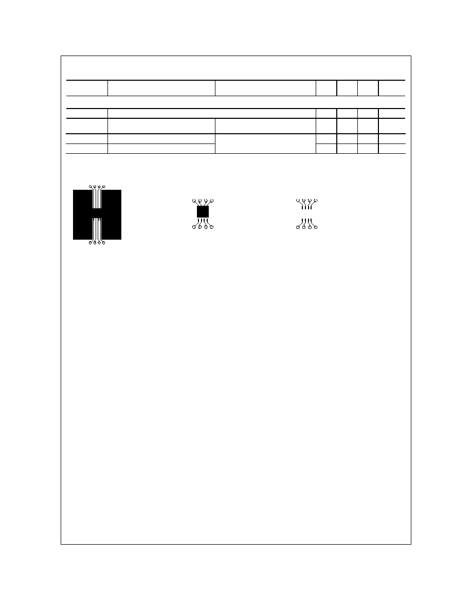
SO-8
D
D
D
G
D2
D2
D1
D1
S2
G2
S1
G1
Pin 1
SO-8
4
3
2
1
5
6
7
8
Q1
Q2
Absolute Maximum Ratings
T
A
=25
o
C unless otherwise noted
Symbol Parameter
Ratings
Units
V
DSS
Drain-Source Voltage
30
V
V
GSS
Gate-Source
Voltage
±
20
V
I
D
Drain Current ≠ Continuous
(Note 1a)
7.5 A
≠
Pulsed
20
Power Dissipation for Single Operation
(Note 1a)
1.6
(Note 1b)
1.0
P
D
(Note 1c)
0.9
W
T
J
, T
STG
Operating and Storage Junction Temperature Range
≠55 to +150
∞
C
Thermal Characteristics
R
JA
Thermal Resistance, Junction-to-Ambient
(Note 1a)
78
∞
C/W
R
JC
Thermal Resistance, Junction-to-Case
(Note 1)
40
∞
C/W
Package Marking and Ordering Information
Device Marking
Device
Reel Size
Tape width
Quantity
FDS6910
FDS6910
13''
12mm
2500 units
FD
S6910
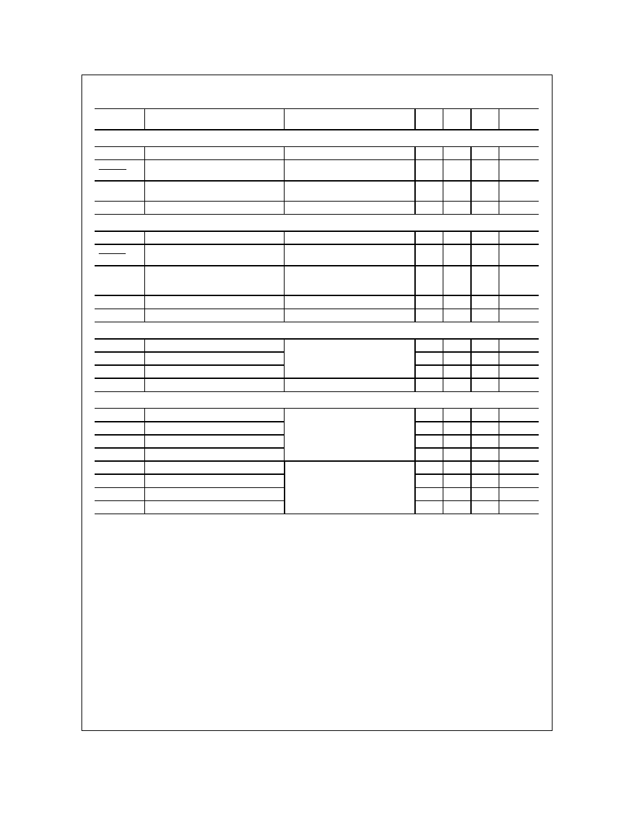
FDS6910 Rev B(W)
Electrical Characteristics
T
A
= 25∞C unless otherwise noted
Symbol Parameter
Test
Conditions
Min Typ
Max
Units
Off Characteristics
BV
DSS
Drain≠Source Breakdown Voltage
V
GS
= 0 V,
I
D
= 250
µ
A
30 V
BV
DSS
T
J
Breakdown Voltage Temperature
Coefficient
I
D
= 250
µ
A, Referenced to 25
∞
C
28 mV/
∞
C
I
DSS
Zero Gate Voltage Drain Current
V
DS
= 24 V, V
GS
= 0 V
V
DS
= 24 V, V
GS
= 0 V, T
J
= 55
∞
C
1
10
µ
A
I
GSS
Gate≠Source
Leakage
V
GS
=
±
20 V, V
DS
= 0 V
±
100
nA
On Characteristics
(Note 2)
V
GS(th)
Gate Threshold Voltage
V
DS
= V
GS
, I
D
= 250
µ
A
1 1.8 3 V
V
GS(th)
T
J
Gate Threshold Voltage
Temperature Coefficient
I
D
= 250
µ
A, Referenced to 25
∞
C
≠4.7 mV/
∞
C
R
DS(on)
Static Drain≠Source
On≠Resistance
V
GS
= 10 V, I
D
= 7.5 A
V
GS
= 4.5 V, I
D
= 6.5 A
V
GS
= 10 V, I
D
= 7.5 A,T
J
= 125
∞
C
10.6
13
14.5
13
1
7
20
m
I
D(on)
On≠State Drain Current
V
GS
= 10 V, V
DS
= 5 V
20
A
g
FS
Forward
Transconductance V
DS
= 5 V,
I
D
= 7.5 A
36
S
Dynamic Characteristics
C
iss
Input
Capacitance
1130
pF
C
oss
Output
Capacitance
300 pF
C
rss
Reverse Transfer Capacitance
V
DS
= 15 V, V
GS
= 0 V,
f = 1.0 MHz
100 pF
R
G
Gate
Resistance
V
GS
= 15 mV, f = 1.0 MHz
2.4
Switching Characteristics
(Note 2)
t
d(on)
Turn≠On Delay Time
9 18 ns
t
r
Turn≠On Rise Time
5 10 ns
t
d(off)
Turn≠Off Delay Time
26 42 ns
t
f
Turn≠Off Fall Time
V
DD
= 15 V, I
D
= 1 A,
V
GS
= 10 V, R
GEN
= 6
7 14 ns
Q
g(TOT)
Total Gate Charge at Vgs=10V
17
24
nC
Q
g
Total Gate Charge at Vgs=5V
9
13
nC
Q
gs
Gate≠Source
Charge
3.1
nC
Q
gd
Gate≠Drain
Charge
V
DD
= 15 V, I
D
= 7.5 A,
2.7 nC
FD
S6910
FDS6910 Rev B(W)
Electrical Characteristics
TA = 25∞C unless otherwise noted
Symbol Parameter
Test
Conditions
Min
Typ
Max
Units
Drain≠Source Diode Characteristics and Maximum Ratings
I
S
Maximum Continuous Drain≠Source Diode Forward Current
1.3
A
V
SD
Drain≠Source Diode Forward
Voltage
V
GS
= 0 V, I
S
= 1.3 A
(Note 2)
1.2 V
t
rr
Diode Reverse Recovery Time
24
nS
Q
rr
Diode Reverse Recovery Charge
I
F
= 7.5 A, d
iF
/d
t
= 100 A/µs
13 nC
Notes:
1. R
JA
is the sum of the junction-to-case and case-to-ambient thermal resistance where the case thermal reference is defined as the solder mounting surface of
the drain pins. R
JC
is guaranteed by design while R
CA
is determined by the user's board design.
a) 78∞C/W when
mounted on a 0.5in
2
pad of 2 oz copper
b) 125∞C/W when
mounted on a 0.02
in
2
pad of 2 oz
copper
c) 135∞C/W when mounted on a
minimum mounting pad.
Scale 1 : 1 on letter size paper
2. Pulse Test: Pulse Width < 300
µ
s, Duty Cycle < 2.0%
FD
S6910
FDS6910 Rev B(W)
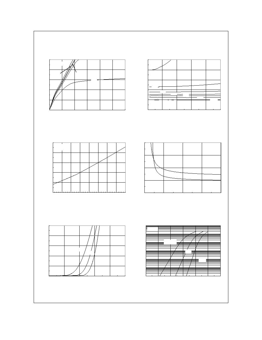
Typical Characteristics
0
4
8
12
16
20
0
0.25
0.5
0.75
1
1.25
1.5
V
DS
, DRAIN-SOURCE VOLTAGE (V)
I
D
,
DRAI
N CURRE
NT (
A
)
3.0V
4.5V
4.0V
V
GS
= 10.0V
3.5V
0.6
1
1.4
1.8
2.2
2.6
0
4
8
12
16
20
I
D
, DRAIN CURRENT (A)
R
DS
(ON)
,
NO
R
M
AL
I
Z
ED
D
RAI
N
-
S
O
UR
CE
ON-
R
E
S
I
S
T
ANC
E
V
GS
= 3.0V
6.0V
5.0
4.5V
4.0
10.0V
3.5V
Figure 1. On-Region Characteristics.
Figure 2. On-Resistance Variation with
Drain Current and Gate Voltage.
0.6
0.8
1
1.2
1.4
1.6
-50
-25
0
25
50
75
100
125
150
T
J
, JUNCTION TEMPERATURE (
o
C)
R
DS
(O
N)
,
NO
RMALI
Z
E
D
DRAI
N-S
O
URCE
O
N
-RE
S
I
S
T
ANCE
I
D
= 7.5A
V
GS
= 10V
0
0.01
0.02
0.03
0.04
2
4
6
8
10
V
GS
, GATE TO SOURCE VOLTAGE (V)
R
DS
(O
N)
, ON
-
R
ESIST
A
N
C
E
(
O
H
M
)
I
D
= 3.8A
T
A
= 125
o
C
T
A
= 25
o
C
Figure 3. On-Resistance Variation with
Temperature.
Figure 4. On-Resistance Variation with
Gate-to-Source Voltage.
0
4
8
12
16
20
1.5
2
2.5
3
3.5
4
V
GS
, GATE TO SOURCE VOLTAGE (V)
I
D
,
DRAI
N CURRE
NT (A)
T
A
= 125
o
C
-55
o
C
V
DS
= 5V
25
o
C
0.0001
0.001
0.01
0.1
1
10
100
0
0.2
0.4
0.6
0.8
1
1.2
V
SD
, BODY DIODE FORWARD VOLTAGE (V)
I
S
,
R
E
V
E
R
S
E
DR
AI
N C
URRE
N
T
(A
)
T
A
= 125
o
C
25
o
C
-55
o
C
V
GS
= 0V
Figure 5. Transfer Characteristics.
Figure 6. Body Diode Forward Voltage Variation
with Source Current and Temperature.
FD
S6910
FDS6910 Rev B(W)
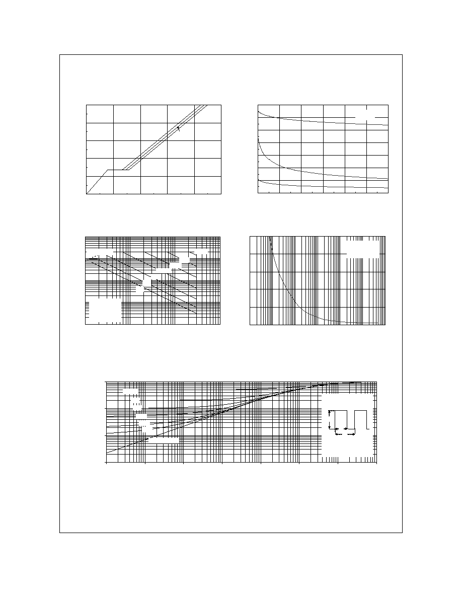
Typical Characteristics
0
2
4
6
8
10
0
4
8
12
16
20
Q
g
, GATE CHARGE (nC)
V
GS
,
G
A
TE
-S
O
URCE
V
O
LTAG
E
(V
)
I
D
= 7.5A
V
DS
= 10V
15V
20V
0
200
400
600
800
1000
1200
1400
0
5
10
15
20
25
30
V
DS
, DRAIN TO SOURCE VOLTAGE (V)
CAP
ACI
TANCE
(pF)
C
iss
C
rss
C
oss
f = 1MHz
V
GS
= 0 V
Figure 7. Gate Charge Characteristics.
Figure 8. Capacitance Characteristics.
0.01
0.1
1
10
100
0.1
1
10
100
V
DS
, DRAIN-SOURCE VOLTAGE (V)
I
D
,
DRAI
N CURRE
NT (A)
DC
10s
1s
100ms
100
µ
s
R
DS(ON)
LIMIT
V
GS
= 10V
SINGLE PULSE
R
JA
= 135
o
C/W
T
A
= 25
o
C
10ms
1ms
0
10
20
30
40
50
0.001
0.01
0.1
1
10
100
1000
t
1
, TIME (sec)
P(p
k),
P
E
A
K
T
R
A
N
S
I
EN
T
POW
E
R
(W
)
SINGLE PULSE
R
JA
= 135∞C/W
T
A
= 25∞C
Figure 9. Maximum Safe Operating Area.
Figure 10. Single Pulse Maximum
Power Dissipation.
0.001
0.01
0.1
1
0.0001
0.001
0.01
0.1
1
10
100
1000
t
1
, TIME (sec)
r
(
t
)
,
NORM
AL
I
Z
ED E
F
F
E
CT
I
V
E
T
RAN
SI
ENT
T
H
ERM
A
L
RE
SI
ST
ANCE
R
JA
(t) = r(t) * R
JA
R
JA
= 135∞C/W
T
J
- T
A
= P * R
JA
(t)
Duty Cycle, D = t
1
/ t
2
P(pk)
t
1
t
2
SINGLE PULSE
0.01
0.02
0.05
0.1
0.2
D = 0.5
Figure 11. Transient Thermal Response Curve.
Thermal characterization performed using the conditions described in Note 1c.
Transient thermal response will change depending on the circuit board design.
FD
S6910