 | –≠–ª–µ–∫—Ç—Ä–æ–Ω–Ω—ã–π –∫–æ–º–ø–æ–Ω–µ–Ω—Ç: FDS6993 | –°–∫–∞—á–∞—Ç—å:  PDF PDF  ZIP ZIP |
June 2003
©
2003 Fairchild Semiconductor Corporation
FDS6993 Rev C (W)
FDS6993
Dual P-Channel PowerTrench
Æ
MOSFET
General Description
These P-Channel MOSFETs are made
using FSC's PowerTrench
Æ
technology.
They are packaged in a single SO-8 which is
designed to allow two MOSFETs to operate
independenly, each with it's own heat sink.
The combination of silicon and package
technologies results in minimum board
space and cost.
Features
∑
Q1:
P-Channel
≠4.3A, ≠30V R
DS(on)
= 55m
@ V
GS
= ≠10V
R
DS(on)
= 85m
@ V
GS
= ≠4.5V
∑
Q2:
P-Channel
≠6.8A, ≠12V R
DS(on)
= 17m
@ V
GS
= ≠4.5V
R
DS(on)
= 24m
@ V
GS
= ≠2.5V
R
DS(on)
= 30m
@ V
GS
= ≠1.8V
∑
High power and handling capability in a widely
used surface mount package
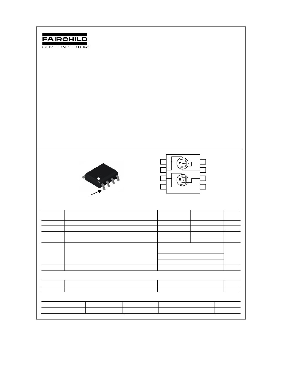
S
D
S
S
SO-8
D
D
D
G
D1
D1
D2
D2
S1
G1
S2
G2
Pin 1
SO-8
Absolute Maximum Ratings
T
A
= 25∞C unless otherwise noted
Symbol
Parameter
Q1
Q2
Units
V
DSS
Drain-Source Voltage
≠30
≠12
V
V
GSS
Gate-Source Voltage
±
25
±
8
V
I
D
Drain Current - Continuous
(Note 1a)
≠4.3
≠6.8
A
- Pulsed
≠20
≠20
P
D
Power Dissipation for Dual Operation
2
W
Power Dissipation for Single Operation
(Note 1a)
1.6
(Note 1b)
1
(Note 1c)
0.9
T
J
, T
STG
Operating and Storage Junction Temperature Range
≠55 to +150
∞
C
Thermal Characteristics
R
JA
Thermal Resistance, Junction-to-Ambient
(Note 1a)
78
∞
C/W
R
JC
Thermal Resistance, Junction-to-Case
(Note 1)
40
∞
C/W
Package Marking and Ordering Information
Device Marking
Device
Reel Size
Tape width
Quantity
FDS6993
FDS6993
13"
12mm
2500 units
4
3
2
1
5
6
7
8
Q2
Q1
FDS6993

FDS6993 Rev C (W)
Electrical Characteristics
T
A
= 25∞C unless otherwise noted
Symbol
Parameter
Test Conditions
Type
Min
Typ Max Units
Off Characteristics
BV
DSS
Drain-Source Breakdown
Voltage
V
GS
= 0 V, I
D
= ≠250
µ
A
V
GS
= 0 V, I
D
= ≠250
µ
A
Q1
Q2
≠30
≠12
V
BV
DSS
T
J
Breakdown Voltage
Temperature Coefficient
I
D
= ≠250
µ
A, Referenced to 25
∞
C
I
D
= ≠250 µA, Referenced to 25
∞
C
Q1
Q2
≠21
≠0.9
mV/
∞
C
I
DSS
Zero Gate Voltage Drain
Current
V
DS
= ≠24 V, V
GS
= 0 V
V
DS
= ≠10 V, V
GS
= 0 V
Q1
Q2
≠1
≠1
µ
A
I
GSS
Gate-Body Leakage
V
GS
= ±25 V, V
DS
= 0 V
V
GS
= ±8 V, V
DS
= 0 V
Q1
Q2
±100
±100
nA
On Characteristics
(Note 2)
V
GS(th)
Gate Threshold Voltage
V
DS
= V
GS
, I
D
= ≠250
µ
A
V
DS
= V
GS
, I
D
= ≠250 µA
Q1
Q2
≠1
≠0.4
≠1.8
≠0.5
≠3
≠1.5
V
V
GS(th)
T
J
Gate Threshold Voltage
Temperature Coefficient
I
D
= ≠250
µ
A, Referenced to 25
∞
C
I
D
= ≠250 µA, Referenced to 25
∞
C
Q1
Q2
4
3
mV/
∞
C
V
GS
= ≠10 V, I
D
= ≠4.3 A
V
GS
= ≠10 V, I
D
= ≠4.3 A, T
J
= 125
∞
C
V
GS
= ≠4.5 V, I
D
= ≠3.4 A
Q1
48
64
74
55
80
85
m
R
DS(on)
Static Drain-Source
On-Resistance
V
GS
= ≠4.5 V, I
D
= ≠6.8 A
V
GS
= ≠4.5 V, I
D
= ≠6.8 A, T
J
= 125
∞
C
V
GS
= ≠2.5 V, I
D
= ≠5.9 A
V
GS
= ≠1.8 V, I
D
= ≠5.0
Q2
11
14
14
19
17
24
24
30
I
D(on)
On-State Drain Current
V
GS
= ≠10 V, V
DS
= ≠5 V
V
GS
= ≠4.5 V, V
DS
= ≠5 V
Q1
Q2
≠20
≠20
A
g
FS
Forward Transconductance
V
DS
= ≠10 V, I
D
= ≠7 A
V
DS
= ≠5 V, I
D
= ≠5 A
Q1
Q2
9
34
S
Dynamic Characteristics
C
iss
Input Capacitance
Q1
Q2
530
2980
pF
C
oss
Output Capacitance
Q1
Q2
140
1230
pF
C
rss
Reverse Transfer Capacitance
Q1
V
DS
= ≠15 V, V
GS
= 0 V, f = 1.0 MHz
Q2
V
DS
= ≠6 V, V
GS
= 0 V, f = 1.0 MHz
Q1
Q2
70
790
pF
FDS6993

FDS6993 Rev C (W)
Electrical Characteristics
(continued)
T
A
= 25∞C unless otherwise noted
Symbol
Parameter
Test Conditions
Type
Min
Typ
Max
Units
Switching Characteristics
(Note 2)
t
d(on)
Turn-On Delay Time
Q1
Q2
10
19
19
34
ns
t
r
Turn-On Rise Time
Q1
Q2
14
20
26
35
ns
t
d(off)
Turn-Off Delay Time
Q1
Q2
14
134
24
215
ns
t
f
Turn-Off Fall Time
Q1
V
DD
= ≠15 V, I
D
= ≠1 A,
V
GS
= ≠10V, R
GEN
= 6
Q2
V
DD
= ≠6 V, I
D
= ≠1 A,
V
GS
= ≠4.5V, R
GEN
= 6
Q1
Q2
9
121
18
193
ns
Q
g
Total Gate Charge
Q1
Q2
5.5
32
7.7
45
nC
Q
gs
Gate-Source Charge
Q1
Q2
1.8
4.0
nC
Q
gd
Gate-Drain Charge
Q1
V
DS
= ≠15 V, I
D
= ≠4.3 A,
V
GS
= ≠5 V
Q2
V
DS
= ≠6 V, I
D
= ≠6.8 A,
V
GS
= ≠5 V
Q1
Q2
2.2
8.0
nC
Drain≠Source Diode Characteristics and Maximum Ratings
I
S
Maximum Continuous Drain-Source Diode Forward Current
Q1
Q2
≠1.3
≠1.3
A
V
SD
Drain-Source Diode Forward
Voltage
V
GS
= 0 V, I
S
= ≠1.3 A
(Note 2)
V
GS
= 0 V, I
S
= ≠1.3 A
(Note 2)
Q1
Q2
≠0.8
≠0.6
≠1.2
≠1.2
V
Notes:
1. R
JA
is the sum of the junction-to-case and case-to-ambient thermal resistance where the case thermal reference is defined as the solder mounting surface of
the drain pins. R
JC
is guaranteed by design while R
CA
is determined by the user's board design.
a) 78∞/W when
mounted on a
0.5 in
2
pad of 2 oz
copper
b) 125∞/W when
mounted on a .02 in
2
pad of 2 oz copper
c) 135∞/W when mounted on a
minimum pad.
Scale 1 : 1 on letter size paper
2. Pulse Test: Pulse Width < 300
µ
s, Duty Cycle < 2.0%
FDS6993
FDS6993 Rev C (W)
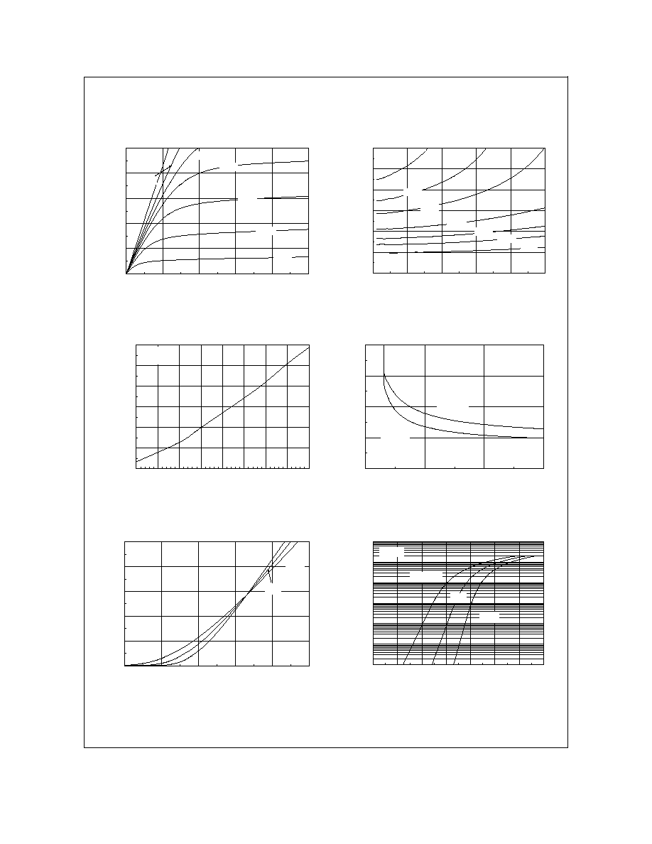
Typical Characteristics: Q1
0
4
8
12
16
20
0
1
2
3
4
5
-V
DS
, DRAIN TO SOURCE VOLTAGE (V)
-I
D
, DRAIN CURRENT (A)
V
GS
= -10V
-3.0V
-3.5V
-4.0V
-4.5V
V
-5.0V
V
-6.0V
V
0.8
1
1.2
1.4
1.6
1.8
2
0
4
8
12
16
20
-I
D
, DRAIN CURRENT (A)
R
DS(ON)
, NORMALIZED
DRAIN-SOURCE ON-RESISTANCE
V
GS
=-4.0V
-4.5V
-6.0V
-7.0V
-8.0V
-10V
-5.0V
Figure 1. On-Region Characteristics.
Figure 2. On-Resistance Variation with
Drain Current and Gate Voltage.
0.8
0.9
1
1.1
1.2
1.3
1.4
-50
-25
0
25
50
75
100
125
150
T
J
, JUNCTION TEMPERATURE (
o
C)
R
DS(ON)
, NORMALIZED
DRAIN-SOURCE ON-RESISTANCE
I
D
= -4.3A
V
GS
= -10V
0
0.05
0.1
0.15
0.2
2.5
5
7.5
10
-V
GS
, GATE TO SOURCE VOLTAGE (V)
R
DS(ON)
, ON-RESISTANCE (OHM)
I
D
= -2.15A
T
A
= 125
o
C
T
A
= 25
o
C
Figure 3. On-Resistance Variation with
Temperature.
Figure 4. On-Resistance Variation with
Gate-to-Source Voltage.
0
3
6
9
12
15
2
2.5
3
3.5
4
4.5
-V
GS
, GATE TO SOURCE VOLTAGE (V)
-I
D
, DRAIN CURRENT (A)
T
A
= -55
o
C
25
o
C
125
o
C
V
DS
= -5V
0.0001
0.001
0.01
0.1
1
10
100
0
0.2
0.4
0.6
0.8
1
1.2
1.4
-V
SD
,
BODY DIODE FORWARD VOLTAGE (V)
-I
S
, REVERSE DRAIN CURRENT (A)
V
GS
=0V
T
A
= 125
o
C
25
o
C
-55
o
C
Figure 5. Transfer Characteristics.
Figure 6. Body Diode Forward Voltage Variation
with Source Current and Temperature.
FDS6993

FDS6993 Rev C (W)
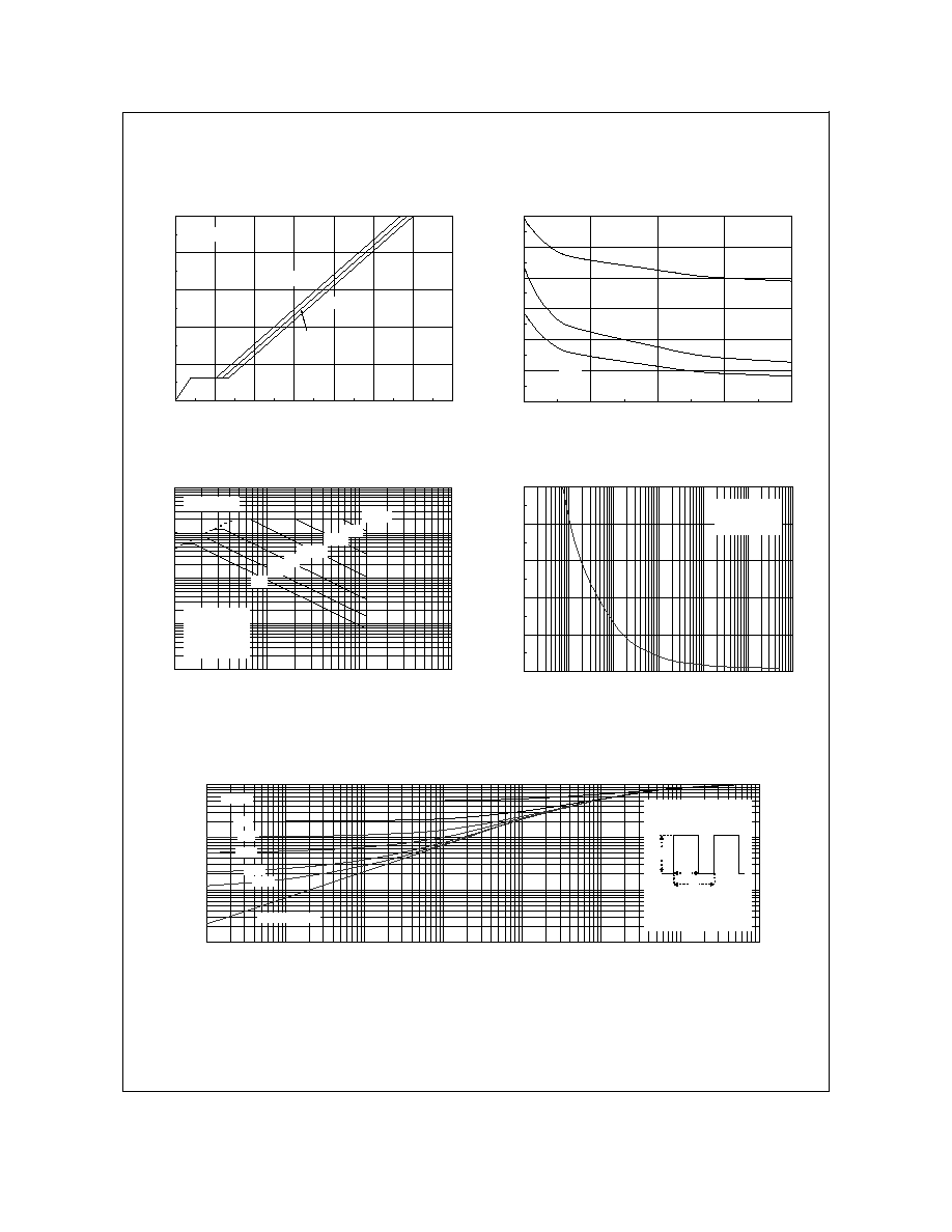
Typical Characteristics: Q1
0
2
4
6
8
10
0
2
4
6
8
10
12
Q
g
, GATE CHARGE (nC)
-V
GS
, GATE-SOURCE VOLTAGE (V)
I
D
= -4.3A
V
DS
= -10V
-20V
-15V
0
100
200
300
400
500
600
700
0
5
10
15
20
25
30
-V
DS
, DRAIN TO SOURCE VOLTAGE (V)
CAPACITANCE (pF)
C
iss
C
oss
C
rss
f = 1 MHz
V
GS
= 0 V
Figure 7. Gate Charge Characteristics.
Figure 8. Capacitance Characteristics.
0.01
0.1
1
10
100
0.1
1
10
100
-V
DS
, DRAIN-SOURCE VOLTAGE (V)
-I
D
, DRAIN CURRENT (A)
DC
1s
100ms
100
µ
s
R
DS(ON)
LIMIT
V
GS
= -10V
SINGLE PULSE
R
JA
= 135
o
C/W
T
A
= 25
o
C
10ms
1ms
10s
0
10
20
30
40
50
0.001
0.01
0.1
1
10
100
1000
t
1
, TIME (sec)
P(pk), PEAK TRANSIENT POWER (W)
SINGLE PULSE
R
JA
= 135∞C/W
T
A
= 25∞C
Figure 9. Maximum Safe Operating Area.
Figure 10. Single Pulse Maximum
Power Dissipation.
0.001
0.01
0.1
1
0.0001
0.001
0.01
0.1
1
10
100
1000
t
1
, TIME (sec)
r(t), NORMALIZED EFFECTIVE TRANSIENT
THERMAL RESISTANCE
R
JA
(t) = r(t) * R
JA
R
JA
= 135
o
C/W
T
J
- T
A
= P * R
JA
(t)
Duty Cycle, D = t
1
/ t
2
P(pk)
t
1
t
2
SINGLE PULSE
0.01
0.02
0.05
0.1
0.2
D = 0.5
Figure 11. Transient Thermal Response Curve.
Thermal characterization performed using the conditions described in Note 1c.
Transient thermal response will change depending on the circuit board design.
FDS6993

FDS6993 Rev C (W)
Typical Characteristics: Q2
0
4
8
12
16
20
0
0.5
1
1.5
2
-V
DS
, DRAIN TO SOURCE VOLTAGE (V)
-I
D
, DRAIN CURRENT (A)
V
GS
= -4.5V
-2.5V
-2.0V
-1.5V
-3.5V
0.8
1
1.2
1.4
1.6
1.8
2
2.2
0
4
8
12
16
20
-I
D
, DRAIN CURRENT (A)
R
DS(ON)
, NORMALIZED
DRAIN-SOURCE ON-RESISTANCE
V
GS
= - 2.0V
-4.5V
-3.0V
-3.5V
-2.5V
-10.0V
-6.0V
Figure 12. On-Region Characteristics.
Figure 13. On-Resistance Variation with
Drain Current and Gate Voltage.
0.8
0.9
1
1.1
1.2
1.3
1.4
-50
-25
0
25
50
75
100
125
150
T
J
, JUNCTION TEMPERATURE (
o
C)
R
DS(ON)
, NORMALIZED
DRAIN-SOURCE ON-RESISTANCE
I
D
= -6.8A
V
GS
= - 4.5V
0.005
0.015
0.025
0.035
0.045
1
2
3
4
5
-V
GS
, GATE TO SOURCE VOLTAGE (V)
R
DS(ON)
, ON-RESISTANCE (OHM)
I
D
= -3.4A
T
A
= 125
o
C
T
A
= 25
o
C
Figure 14. On-Resistance Variation with
Temperature.
Figure 15. On-Resistance Variation with
Gate-to-Source Voltage.
0
4
8
12
16
20
0
0.4
0.8
1.2
1.6
2
-V
GS
, GATE TO SOURCE VOLTAGE (V)
-I
D
, DRAIN CURRENT (A)
T
A
= 125
o
C
25
o
C
-55
o
C
V
DS
= -5V
0.0001
0.001
0.01
0.1
1
10
0
0.2
0.4
0.6
0.8
1
-V
SD
,
BODY DIODE FORWARD VOLTAGE (V)
-I
S
, REVERSE DRAIN CURRENT (A)
V
GS
= 0V
T
A
= 125
o
C
25
o
C
-55
o
C
Figure 16. Transfer Characteristics.
Figure 17. Body Diode Forward Voltage Variation
with Source Current and Temperature.
FDS6993
FDS6993 Rev C (W)
Typical Characteristics: Q2
0
2
4
6
8
10
0
10
20
30
40
50
60
70
Q
g
, GATE CHARGE (nC)
-V
GS
, GATE-SOURCE VOLTAGE (V)
I
D
= -6.8A
V
DS
= -4V
-8V
-6V
0
700
1400
2100
2800
3500
4200
0
3
6
9
12
-V
DS
, DRAIN TO SOURCE VOLTAGE (V)
CAPACITANCE (pF)
C
iss
C
oss
C
rss
f = 1 MHz
V
GS
= 0 V
Figure 18. Gate Charge Characteristics.
Figure 19. Capacitance Characteristics.
0.01
0.1
1
10
100
0.1
1
10
100
-V
DS
, DRAIN-SOURCE VOLTAGE (V)
-I
D
, DRAIN CURRENT (A)
DC
10s
1s
100ms
100
µ
s
R
DS(ON)
LIMIT
V
GS
= -4.5V
SINGLE PULSE
R
JA
= 135
o
C/W
T
A
= 25
o
C
10ms
1ms
0
10
20
30
40
50
0.001
0.01
0.1
1
10
100
1000
t
1
, TIME (sec)
P(pk), PEAK TRANSIENT POWER (W)
SINGLE PULSE
R
JA
= 135∞C/W
T
A
= 25∞C
Figure 20. Maximum Safe Operating Area.
Figure 21. Single Pulse Maximum
Power Dissipation.
0.001
0.01
0.1
1
0.0001
0.001
0.01
0.1
1
10
100
1000
t
1
, TIME (sec)
r(t), NORMALIZED EFFECTIVE
TRANSIENT THERMAL RESISTANCE
R
JA
(t) = r(t) * R
JA
R
JA
= 135
o
C/W
T
J
- T
A
= P * R
JA
(t)
Duty Cycle, D = t
1
/ t
2
P(pk)
t
1
t
2
SINGLE PULSE
0.01
0.02
0.05
0.1
0.2
D = 0.5
Figure 22. Transient Thermal Response Curve.
Thermal characterization performed using the conditions described in Note 1c.
Transient thermal response will change depending on the circuit board design.
FDS6993

FDS6993 Rev C (W)