 | ÐлекÑÑоннÑй компоненÑ: FDS6994S | СкаÑаÑÑ:  PDF PDF  ZIP ZIP |
Äîêóìåíòàöèÿ è îïèñàíèÿ www.docs.chipfind.ru
April 2002
PRELIMINARY
2002 Fairchild Semiconductor Corporation
FDS6994S Rev B(W)
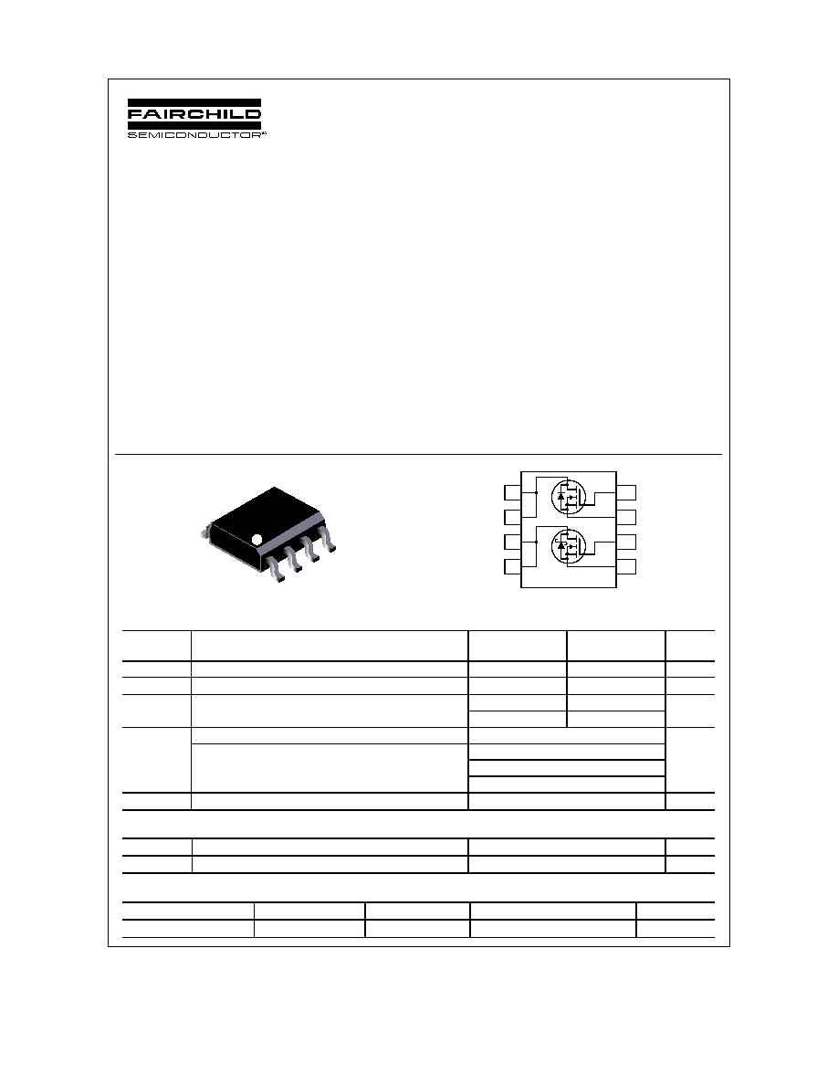
FDS6994S
Dual Notebook Power Supply N-Channel PowerTrench
SyncFET
TM
General Description
The FDS6994S is designed to replace two single SO-8
MOSFETs and Schottky diode in synchronous DC:DC
power supplies that provide various peripheral voltages
for notebook computers and other battery powered
electronic devices. FDS6994S contains two unique
30V, N-channel, logic level, PowerTrench MOSFETs
designed to maximize power conversion efficiency.
The high-side switch (Q1) is designed with specific
emphasis on reducing switching losses while the low-
side switch (Q2) is optimized to reduce conduction
losses. Q2 also includes an integrated Schottky diode
using Fairchild's monolithic SyncFET technology.
Features
·
Q2:
Optimized to minimize conduction losses
Includes SyncFET Schottky body diode
8.2A, 30V
R
DS(on)
= 15.0 m
@ V
GS
= 10V
R
DS(on)
= 17.5 m
@ V
GS
= 4.5V
·
Q1:
Optimized for low switching losses
Low gate charge (8.0 nC typical)
6.9A, 30V
R
DS(on)
= 21.0 m
@ V
GS
= 10V
R
DS(on)
= 26.0 m
@ V
GS
= 4.5V
S2
SO-8
G2
S1
G1
D2
D2
D1
D1
4
3
2
1
5
6
7
8
Q1
Q2
Absolute Maximum Ratings
T
A
= 25°C unless otherwise noted
Symbol Parameter
Q2
Q1 Units
V
DSS
Drain-Source
Voltage
30
30
V
V
GSS
Gate-Source
Voltage
±16
±16
V
I
D
Drain Current - Continuous
(Note 1a)
8.2
6.9 A
-
Pulsed
30
20
P
D
Power Dissipation for Dual Operation
2
W
Power Dissipation for Single Operation
(Note 1a)
1.6
(Note 1b)
1
(Note 1c)
0.9
T
J
, T
STG
Operating and Storage Junction Temperature Range
55 to +150
°C
Thermal Characteristics
R
JA
Thermal Resistance, Junction-to-Ambient
(Note 1a)
78
°C/W
R
JC
Thermal Resistance, Junction-to-Case
(Note 1)
40
°C/W
Package Marking and Ordering Information
Device Marking
Device
Reel Size
Tape width
Quantity
FDS6994S FDS6994S 13"
12mm
2500
units
FDS6994S
FDS6994S Rev B (W)
Electrical Characteristics
T
A
= 25°C unless otherwise noted
Symbol
Parameter Test
Conditions
Type
Min
Typ Max Units
Off Characteristics
BV
DSS
Drain-Source Breakdown
Voltage
V
GS
= 0 V, I
D
= 1 mA
V
GS
= 0 V, I
D
= 250 uA
Q2
Q1
30
30
V
BV
DSS
T
J
Breakdown Voltage
Temperature Coefficient
I
D
= 1 mA, Referenced to 25
°C
I
D
= 250 µA, Referenced to 25
°C
Q2
Q1
23
22
mV/
°C
I
DSS
Zero Gate Voltage Drain
Current
V
DS
= 24 V, V
GS
= 0 V
Q2
Q1
500
1
µA
I
GSS
Gate-Body
Leakage V
GS
=
±16 V, V
DS
= 0 V
All
±100
nA
On Characteristics
(Note 2)
V
GS(th)
Gate Threshold Voltage
V
DS
= V
GS
, I
D
= 1 mA
V
DS
= V
GS
, I
D
= 250 µA
Q2
Q1
1
1
1.5
1.9
3
3
V
V
GS(th)
T
J
Gate Threshold Voltage
Temperature Coefficient
I
D
= 1 mA, Referenced to 25
°C
I
D
= 250 uA, Referenced to 25
°C
Q2
Q1
2
4
mV/
°
C
V
GS
= 10 V, I
D
= 8.2A
V
GS
= 10 V, I
D
= 8.2 A, T
J
= 125
°C
V
GS
= 4.5 V, I
D
= 7.6 A
Q2
10
15
11
15
24
18
R
DS(on)
Static Drain-Source
On-Resistance
V
GS
= 10 V, I
D
= 6.9 A
V
GS
= 10 V, I
D
= 6.9 A, T
J
= 125
°C
V
GS
= 4.5 V, I
D
= 6.2 A
Q1 18
26
21
21
34
26
m
Dynamic Characteristics
C
iss
Input
Capacitance
Q2
Q1
2762
771
pF
C
oss
Output
Capacitance
Q2
Q1
534
208
pF
C
rss
Reverse
Transfer
Capacitance
V
DS
= 15 V, V
GS
= 0 V,
f = 1.0 MHz
Q2
Q1
199
84
pF
R
g
Gate
Resistance V
GS
= 15 mV, f = 1.0 MHz
Q2
Q1
1.7
2.5
Switching Characteristics
(Note 2)
t
d(on)
Turn-On Delay Time
Q2
Q1
10
8
20
15
ns
t
r
Turn-On Rise Time
Q2
Q1
8
5
17
9
ns
t
d(off)
Turn-Off Delay Time
Q2
Q1
46
25
70
40
ns
t
f
Turn-Off Fall Time
V
DD
= 15 V, I
D
= 1 A,
V
GS
= 10V, R
GEN
= 6
Q2
Q1
17
5
30
9
ns
Q
g
Total Gate Charge
Q2
Q1
25
8
35
12
nC
Q
gs
Gate-Source
Charge
Q2
Q1
6
2
nC
Q
gd
Gate-Drain
Charge
Q2:
V
DS
= 15 V, I
D
= 8.2 A, V
GS
= 5 V
Q1:
V
DS
= 15 V, I
D
= 6.9 A, V
GS
= 5 V
Q2
Q1
7
3
nC
FDS6994S
FDS6994S Rev B (W)
Electrical Characteristics
(continued)
T
A
= 25°C unless otherwise noted
Symbol
Parameter
Test Conditions
Type
Min
Typ
Max
Units
DrainSource Diode Characteristics and Maximum Ratings
I
S
Maximum Continuous Drain-Source Diode Forward Current
Q2
Q1
2.3
1.3
A
t
RR
Reverse
Recovery
Time
25
ns
Q
RR
Reverse
Recovery
Charge
I
F
= 8.2 A,
d
iF
/d
t
= 300 A/µs
(Note
3)
Q2
39 nC
t
RR
Reverse
Recovery
Time
21
ns
Q
RR
Reverse
Recovery
Charge
I
F
= 6.9 A,
d
iF
/d
t
= 100 A/µs
(Note
3)
Q1
31 nC
V
SD
Drain-Source
Diode
Forward
Voltage
V
GS
= 0 V, I
S
= 2.3 A
(Note
2)
V
GS
= 0 V, I
S
= 5.0 A
(Note
2)
V
GS
= 0 V, I
S
= 1.3 A
(Note
2)
Q2
Q2
Q1
400
520
740
700
800
1200
mV
Notes:
1. R
JA
is the sum of the junction-to-case and case-to-ambient thermal resistance where the case thermal reference is defined as the solder mounting surface of
the drain pins. R
JC
is guaranteed by design while R
CA
is determined by the user's board design.
a) 78°C/W
when
mounted on a
0.5in
2
pad of 2
oz copper
b) 125°C/W
when
mounted on a
0.02 in
2
pad of
2 oz copper
c) 135°C/W
when
mounted on a
minimum pad.
Scale 1 : 1 on letter size paper
2. Pulse Test: Pulse Width < 300
µs, Duty Cycle < 2.0%
3. See "SyncFET Schottky body diode characteristics" below.
FDS6994S
FDS6994S Rev B (W)
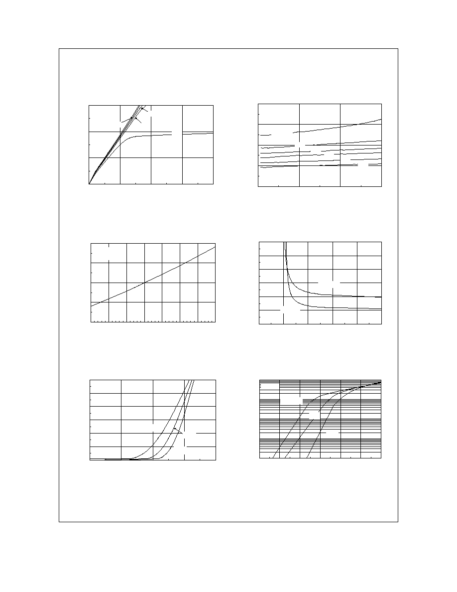
Typical Characteristics for Q2
0
10
20
30
0
0.5
1
1.5
2
V
DS
, DRAIN-SOURCE VOLTAGE (V)
I
D
, DRAIN CURRE
NT (A)
4.5V
3.5V
V
GS
= 10V
3.0V
2.5V
0.8
1
1.2
1.4
1.6
0
10
20
30
I
D
, DRAIN CURRENT (A)
R
DS
(
O
N)
,
NO
RMALI
Z
E
D
DRAI
N-
S
O
URCE
O
N
-
R
E
S
I
S
T
ANCE
V
GS
= 3.0V
6.0V
10V
4.5V
3.5V
4.0V
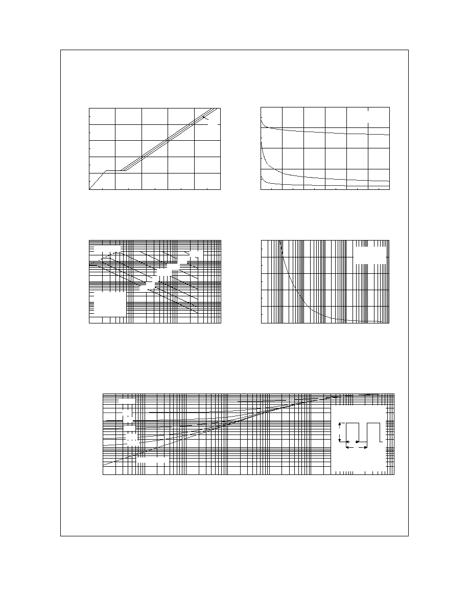
Figure 1. On-Region Characteristics.
Figure 2. On-Resistance Variation with
Drain Current and Gate Voltage.
0.6
0.8
1
1.2
1.4
-50
-25
0
25
50
75
100
125
T
J
, JUNCTION TEMPERATURE (
o
C)
R
DS
(
O
N)
,
NO
RMALI
Z
E
D
DRAI
N-
S
O
URCE
O
N
-
R
E
S
I
S
TANCE
I
D
= 8.2A
V
GS
= 10V
0.005
0.01
0.015
0.02
0.025
0.03
0.035
0
2
4
6
8
10
V
GS
, GATE TO SOURCE VOLTAGE (V)
R
DS
(
O
N)
,
O
N
-
R
E
S
I
S
T
ANCE
(
O
HM)
I
D
= 4.1A
T
A
= 125
o
C
T
A
= 25
o
C
Figure 3. On-Resistance Variation with
Temperature.
Figure 4. On-Resistance Variation with
Gate-to-Source Voltage.
0
5
10
15
20
25
30
1
1.5
2
2.5
3
V
GS
, GATE TO SOURCE VOLTAGE (V)
I
D
, DRAIN CURRE
NT (
A
)
T
A
= 125
o
C
25
o
C
-55
o
C
V
DS
= 5V
0.001
0.01
0.1
1
10
0
0.1
0.2
0.3
0.4
0.5
0.6
V
SD
, BODY DIODE FORWARD VOLTAGE (V)
I
S
, R
EVER
SE
DRAI
N CURRE
NT (A)
T
A
= 125
o
C
25
o
C
-55
o
C
V
GS
= 0V
Figure 5. Transfer Characteristics.
Figure 6. Body Diode Forward Voltage Variation
with Source Current and Temperature.
FDS6994S
FDS6994S Rev B (W)
Typical Characteristics for Q2
0
2
4
6
8
10
0
10
20
30
40
50
Q
g
, GATE CHARGE (nC)
V
GS
, G
A
TE
-
S
O
URCE
V
O
LTAG
E
(
V
)
I
D
=8.2A
V
DS
= 10V
20V
15V
0
1000
2000
3000
4000
0
5
10
15
20
25
30
V
DS
, DRAIN TO SOURCE VOLTAGE (V)
CAP
ACITANCE
(
p
F
)
C
iss
C
rss
C
oss
f = 1MHz
V
GS
= 0 V
Figure 7. Gate Charge Characteristics.
Figure 8. Capacitance Characteristics.
0.01
0.1
1
10
100
0.1
1
10
100
V
DS
, DRAIN-SOURCE VOLTAGE (V)
I
D
, DRAIN CURRE
NT (
A
)
DC
10s
1s
100ms
100µs
R
DS(ON)
LIMIT
V
GS
= 10V
SINGLE PULSE
R
JA
= 135
o
C/W
T
A
= 25
o
C
10ms
1ms
0
10
20
30
40
50
0.001
0.01
0.1
1
10
100
1000
t
1
, TIME (sec)
P
(
pk
),
P
E
AK TRANS
I
E
NT P
O
W
E
R (W
)
SINGLE PULSE
R
JA
= 135°C/W
T
A
= 25°C
Figure 9. Maximum Safe Operating Area.
Figure 10. Single Pulse Maximum
Power Dissipation.
0.001
0.01
0.1
1
0.0001
0.001
0.01
0.1
1
10
100
1000
t
1
, TIME (sec)
r
(t),
N
O
R
M
A
L
I
Z
E
D
E
FFE
C
T
I
V
E
T
RANS
I
E
NT
T
H
E
R
MAL
RE
S
I
S
T
ANCE
R
JA
(t) = r(t) * R
JA
R
JA
= 135 °C/W
T
J
- T
A
= P * R
JA
(t)
Duty Cycle, D = t
1
/ t
2
P(pk)
t
1
t
2
SINGLE PULSE
0.01
0.02
0.05
0.1
0.2
D = 0.5
Figure 11. Transient Thermal Response Curve.
Thermal characterization performed using the conditions described in Note 1c.
Transient thermal response will change depending on the circuit board design.
FDS6994S