Äîêóìåíòàöèÿ è îïèñàíèÿ www.docs.chipfind.ru
2004 Fairchild Semiconductor Corporation
FDS7066SN3 Rev C2 (W)
January 2004
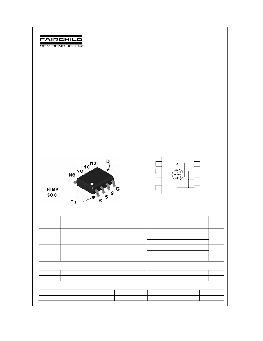
FDS7066SN3
30V N-Channel PowerTrench
SyncFET
TM
General Description
The FDS7066SN3 is designed to replace a single SO-8
FLMP MOSFET and Schottky diode in synchronous
DC:DC power supplies. This 30V MOSFET is designed
to maximize power conversion efficiency, providing a
low R
DS(ON)
and low gate charge. The FDS7066SN3
includes an integrated Schottky diode using Fairchild's
monolithic SyncFET technology. The performance of
the FDS7066SN3 as the low-side switch in a
synchronous rectifier is close to the performance of the
FDS7066N3 in parallel with a Schottky diode.
Applications
· DC/DC converter
· Motor drivesFeatures
Features
· 19 A, 30 V
R
DS(ON)
= 5.5 m
@ V
GS
= 10 V
R
DS(ON)
= 6.0 m
@ V
GS
= 4.5 V
· High performance trench technology for extremely
low R
DS(ON)
· High power and current handling capability
· Fast switching
· FLMP SO-8 package: Enhanced thermal
performance in industry-standard package size
4
5
3
6
2
7
1
8
Bottom-side
Drain Contact
Absolute Maximum Ratings
T
A
=25
o
C unless otherwise noted
Symbol Parameter
Ratings
Units
V
DSS
Drain-Source Voltage
30
V
V
GSS
Gate-Source
Voltage
±16
V
I
D
Drain Current Continuous
(Note 1a)
19 A
Pulsed
60
P
D
Power Dissipation for Single Operation
(Note 1a)
3.0
(Note 1b)
1.7
W
T
J
, T
STG
Operating and Storage Junction Temperature Range
55 to +150
°C
Thermal Characteristics
R
JA
Thermal Resistance, Junction-to-Ambient
(Note 1a)
40
°C/W
R
JC
Thermal Resistance, Junction-to-Case
(Note 1)
0.5
°C/W
Package Marking and Ordering Information
Device Marking
Device
Reel Size
Tape width
Quantity
FDS7066SN3
FDS7066SN3
13''
12mm
2500 units
FDS7066SN3
FDS7066SN3 Rev C2 (W)
Electrical Characteristics
T
A
= 25°C unless otherwise noted
Symbol Parameter
Test
Conditions
Min
Typ
Max
Units
Off Characteristics
BV
DSS
DrainSource Breakdown Voltage V
GS
= 0 V, I
D
= 1 mA
30
V
BV
DSS
T
J
Breakdown Voltage Temperature
Coefficient
I
D
= 10 mA, Referenced to 25
°C
25 mV/
°C
I
DSS
Zero Gate Voltage Drain Current
V
DS
= 24 V, V
GS
= 0 V
500
µA
I
GSS
GateBody
Leakage
V
GS
=
±16 V, V
DS
= 0 V
±100
nA
On Characteristics
(Note 2)
V
GS(th)
Gate Threshold Voltage
V
DS
= V
GS
, I
D
= 1 mA
1
1.4
3
V
V
GS(th)
T
J
Gate Threshold Voltage
Temperature Coefficient
I
D
= 10 mA, Referenced to 25
°C
3 mV/
°C
R
DS(on)
Static DrainSource
OnResistance
V
GS
= 10 V, I
D
= 19 A
V
GS
= 4.5 V, I
D
= 17.5 A
V
GS
= 10 V, I
D
= 19 A, T
J
= 125
°C
4.5
5.0
5.5
6.0
8.0
m
g
FS
Forward
Transconductance V
DS
= 10 V, I
D
= 19 A
98
S
Dynamic Characteristics
C
iss
Input
Capacitance
4740
pF
C
oss
Output
Capacitance
825
pF
C
rss
Reverse Transfer Capacitance
V
DS
= 15 V, V
GS
= 0 V,
f = 1.0 MHz
300 pF
R
G
Gate
Resistance
V
GS
= 15 mV, f = 1.0 MHz
1.4
Switching Characteristics
(Note 2)
t
d(on)
TurnOn
Delay
Time
12
22
ns
t
r
TurnOn Rise Time
12
22
ns
t
d(off)
TurnOff Delay Time
85
136
ns
t
f
TurnOff
Fall
Time
V
DD
= 15 V, I
D
= 1 A,
V
GS
= 10 V, R
GEN
= 6
32 51 ns
Q
g
Total Gate Charge
41
57
nC
Q
gs
GateSource
Charge
10
nC
Q
gd
GateDrain
Charge
V
DS
= 15 V, I
D
= 19 A,
V
GS
= 5.0 V
10 nC
DrainSource Diode Characteristics and Maximum Ratings
I
S
Maximum Continuous DrainSource Schottky Diode Forward Current
4.3
A
V
SD
DrainSource Schottky Diode
Forward Voltage
V
GS
= 0 V, I
S
= 4.3 A
(Note 2)
0.4
0.7 V
t
RR
Reverse
Recovery
Time
26.6
ns
Q
RR
Reverse Recovery Charge
I
F
= 19 A
diF/dt = 300 A/us
28 nC
Notes:
1. R
JA
is the sum of the junction-to-case and case-to-ambient thermal resistance where the case thermal reference is defined as the solder mounting surface of
the drain pins. R
JC
is guaranteed by design while R
CA
is determined by the user's board design.
a) 40°C/W
when
mounted on a 1in
2
pad
of 2 oz copper
b)
85°C/W when mounted on
a minimum pad of 2 oz
copper
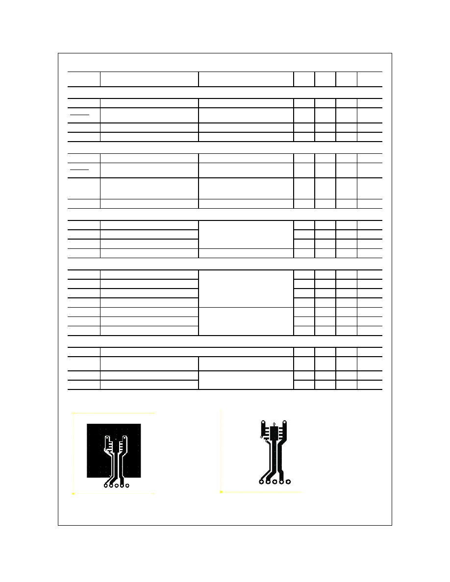
Scale 1 : 1 on letter size paper
2. Pulse Test: Pulse Width < 300
µs, Duty Cycle < 2.0%
FDS7066SN3
FDS7066SN3 Rev C2 (W)
Typical Characteristics
0
10
20
30
40
50
60
0
0.25
0.5
0.75
1
V
DS
, DRAIN TO SOURCE VOLTAGE (V)
I
D
, DRAIN CURRENT
(A)
V
GS
= 10V
2.0V
2.5V
4.5V
3.0V
0.8
1
1.2
1.4
1.6
1.8
2
0
10
20
30
40
50
60
I
D
, DIRAIN CURRENT (A)
R
DS
(O
N)
, NORMAL
IZ
ED
DRAIN-SOURCE ON-RESIST
ANCE
V
GS
= 2.5V
10V
3.0V
4.0V
4.5V
6.0V
3.5V
Figure 1. On-Region Characteristics.
Figure 2. On-Resistance Variation with
Drain Current and Gate Voltage.
0.7
0.9
1.1
1.3
1.5
-50
-25
0
25
50
75
100
125
T
J
, JUNCTION TEMPERATURE (
o
C)
R
DS
(O
N)
, NORMAL
IZ
ED
DRAIN-SOURCE ON-RESIST
ANCE
I
D
= 19A
V
GS
= 10V
0.004
0.008
0.012
0.016
2
4
6
8
10
V
GS
, GATE TO SOURCE VOLTAGE (V)
R
DS
(O
N)
, ON-RESIST
ANCE (OHM)
I
D
= 9.5A
T
A
= 125
o
C
T
A
= 25
o
C
Figure 3. On-Resistance Variation
withTemperature.
Figure 4. On-Resistance Variation with
Gate-to-Source Voltage.
0
10
20
30
40
50
60
1.5
2
2.5
3
V
GS
, GATE TO SOURCE VOLTAGE (V)
I
D
, DRAIN CURRENT
(A)
T
A
= 125
o
C
25
o
C
-55
o
C
V
DS
= 5.0V
0.0001
0.001
0.01
0.1
1
10
0
0.2
0.4
0.6
V
SD
,
BODY DIODE FORWARD VOLTAGE (V)
I
S
, REVERSE DRAIN CURRENT
(A)
V
GS
= 0V
T
A
= 125
o
C
25
o
C
-55
o
C
Figure 5. Transfer Characteristics.
Figure 6. Body Diode Forward Voltage Variation
with Source Current and Temperature.
FDS7066SN3
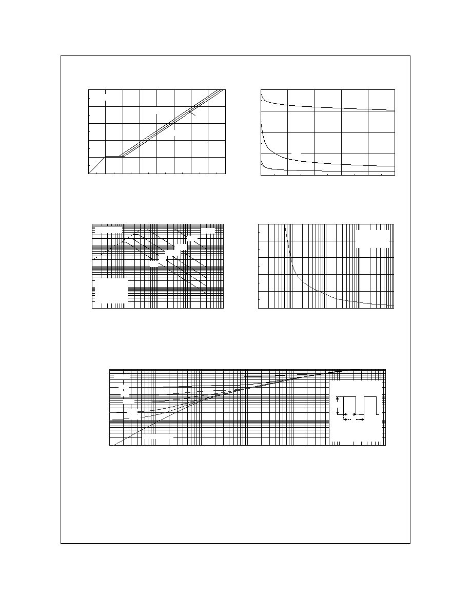
FDS7066SN3 Rev C2 (W)
Typical Characteristics
0
2
4
6
8
10
0
10
20
30
40
50
60
70
80
Q
g
, GATE CHARGE (nC)
V
GS
, GAT
E
-SOURCE VOL
T
A
GE (V)
I
D
= 19A
V
DS
= 10V
15V
20V
0
1500
3000
4500
6000
0
6
12
18
24
30
V
DS
, DRAIN TO SOURCE VOLTAGE (V)
CAPACIT
ANCE (p
F
)
C
iss
C
oss
C
rss
f = 1 MHz
V
GS
= 0 V
Figure 7. Gate Charge Characteristics.
Figure 8. Capacitance Characteristics.
0.01
0.1
1
10
100
0.01
0.1
1
10
100
V
DS
, DRAIN-SOURCE VOLTAGE (V)
I
D
, DRAIN CURRENT
(A)
DC
1s
100ms
100µs
R
DS(ON)
LIMIT
V
GS
= 10V
SINGLE PULSE
R
JA
= 85
o
C/W
T
A
= 25
o
C
10ms
1ms
0
10
20
30
40
50
0.01
0.1
1
10
100
t
1
, TIME (sec)
P(p
k
), PEAK T
RANSIENT
POW
E
R (W
)
SINGLE PULSE
R
JA
= 85°C/W
T
A
= 25°C
Figure 9. Maximum Safe Operating Area.
Figure 10. Single Pulse Maximum
Power Dissipation.
0.001
0.01
0.1
1
0.001
0.01
0.1
1
10
100
1000
t
1
, TIME (sec)
r(t), NORMAL
IZ
ED EF
F
E
CT
IVE
TRANSIENT THERMAL RESISTANCE
R
JA
(t) = r(t) + R
JA
R
JA
= 85
o
C/W
T
J
- T
A
= P * R
JA
(t)
Duty Cycle, D = t
1
/ t
2
P(pk)
t
1
t
2
SINGLE PULSE
0.01
0.02
0.05
0.1
0.2
D = 0.5
Figure 11. Transient Thermal Response Curve.
Thermal characterization performed using the conditions described in Note 1b.
Transient thermal response will change depending on the circuit board design.
FDS7066SN3
FDS7066SN3 Rev C2 (W)
Typical Characteristics
(continued)
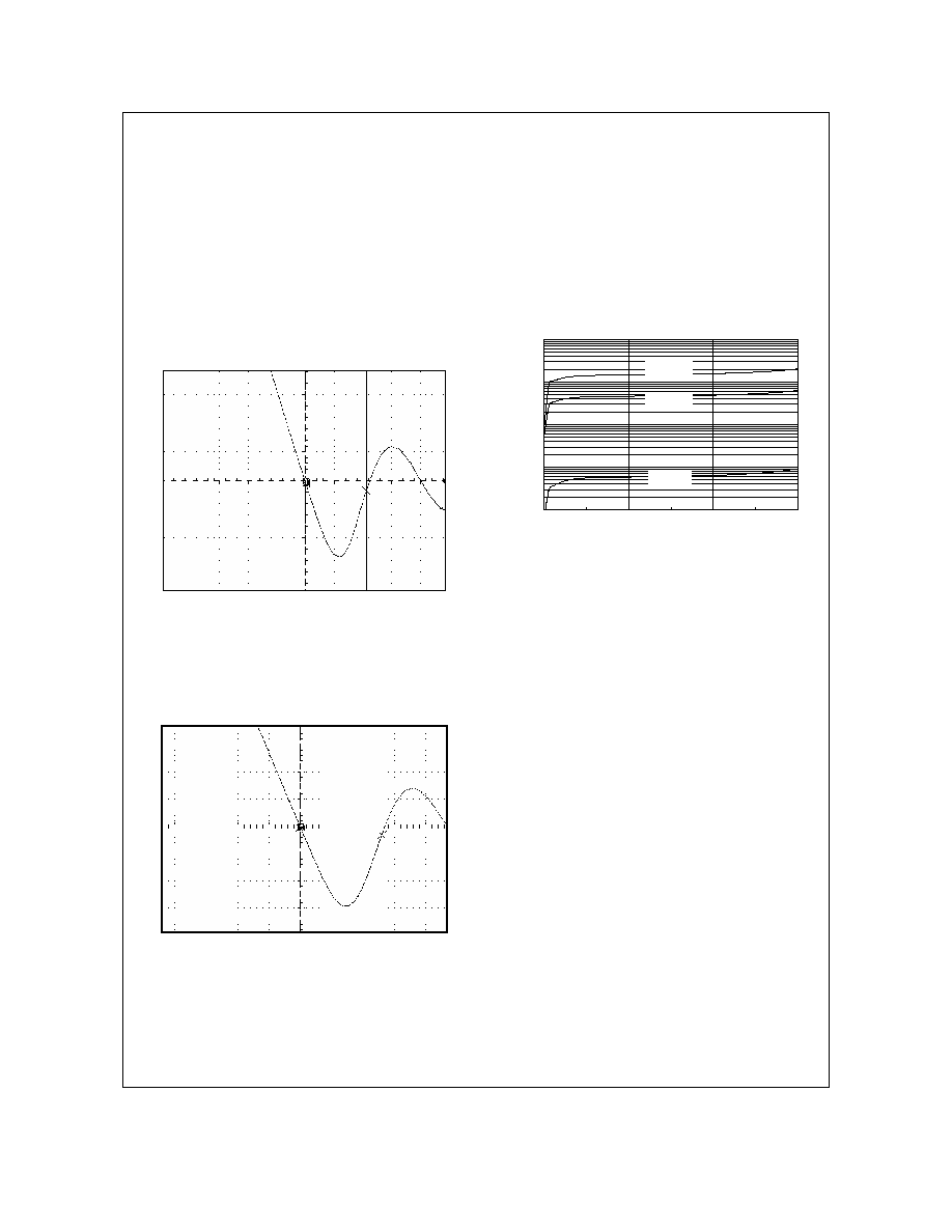
SyncFET Schottky Body Diode
Characteristics
Fairchild's SyncFET process embeds a Schottky diode in
parallel with PowerTrench MOSFET. This diode exhibits
similar characteristics to a discrete external Schottky diode
in parallel with a MOSFET. Figure 12 shows the reverse
recovery characteristic of the FDS7066SN3.
Figure 12. FDS7066SN3 SyncFET body
diode reverse recovery characteristic.
For comparison purposes, Figure 13 shows the reverse
recovery characteristics of the body diode of an equivalent
size MOSFET produced without SyncFET (FDS7066N3).
Figure 13. Non-SyncFET (FDS7066N3) body
diode reverse recovery characteristic.
Schottky barrier diodes exhibit significant leakage at high
temperature and high reverse voltage. This will increase
the power in the device.
0.00001
0.0001
0.001
0.01
0.1
0
10
20
30
V
DS
, REVERSE VOLTAGE (V)
I
DS
S
, REVERSE LEAKAGE CURRENT (A)
T
A
= 100
o
C
T
A
= 25
o
C
T
A
= 125
o
C
Figure 14. SyncFET body diode reverse leakage
versus drain-source voltage and temperature
FDS7066SN3
0.08A/div
12.5 nS/div
0.08A/div
12.5 nS/div