 | –≠–ª–µ–∫—Ç—Ä–æ–Ω–Ω—ã–π –∫–æ–º–ø–æ–Ω–µ–Ω—Ç: FDS8874 | –°–∫–∞—á–∞—Ç—å:  PDF PDF  ZIP ZIP |
August 2005
FDS88
74 N-
Channel
Powe
rTr
enc
h
Æ
MO
SFET
©2005 Fairchild Semiconductor Corporation
FDS8874 Rev. A
www.fairchildsemi.com
1
FDS8874
N-Channel PowerTrench
Æ
MOSFET
30V, 16A, 5.5m
Features
r
DS(ON)
= 5.5m
, V
GS
= 10V, I
D
= 16A
r
DS(ON)
= 7.0m
, V
GS
= 4.5V, I
D
= 15A
High performance trench technology for extremely low
r
DS(ON)
Low gate charge
High power and current handling capability
100% Rg tested
RoHS Compliant
General Description
This N-Channel MOSFET has been designed specifically to
improve the overall efficiency of DC/DC converters using
either synchronous or conventional switching PWM
controllers. It has been optimized for low gate charge, low
r
DS(ON)
and fast switching speed.
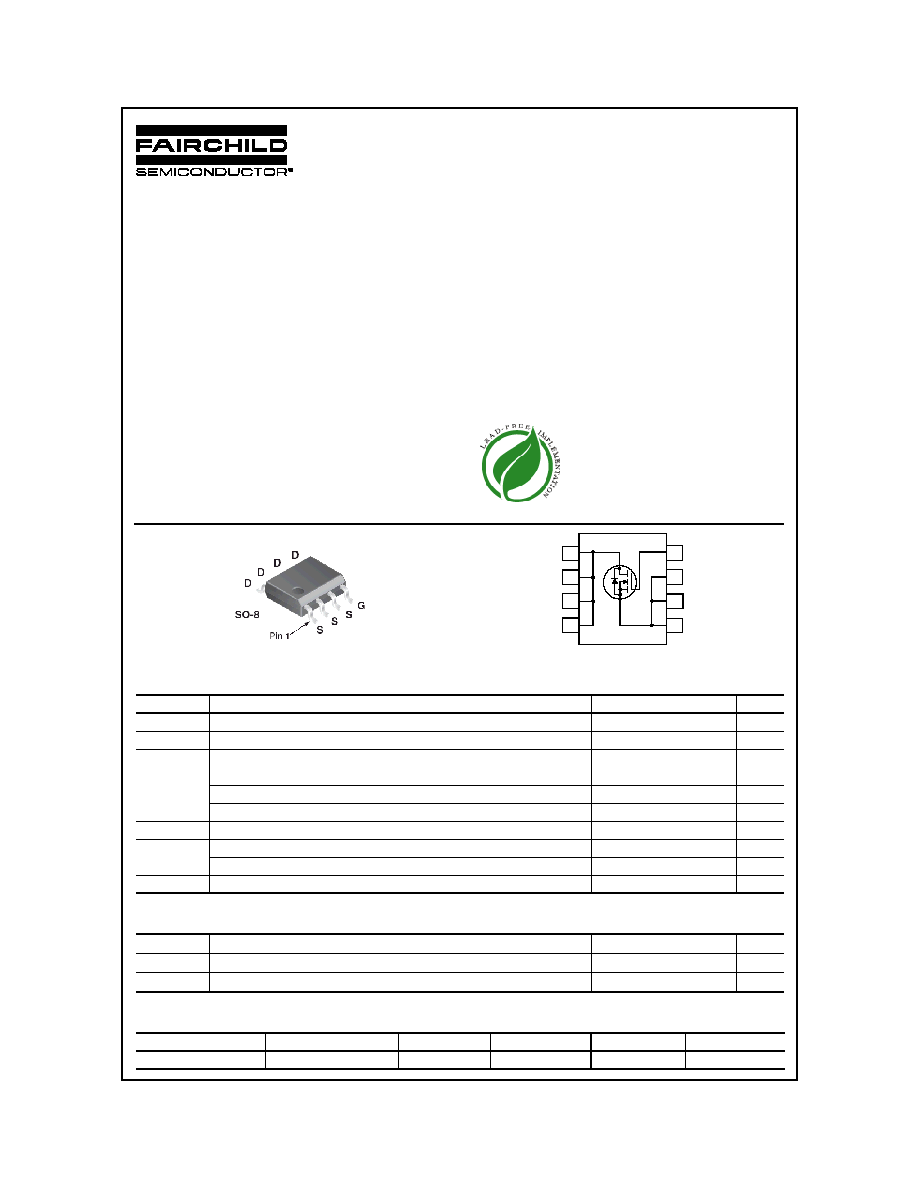
5
8
7
6
1
2
3
4
MOSFET Maximum Ratings
T
A
= 25∞C unless otherwise noted
Thermal Characteristics
Package Marking and Ordering Information
Symbol
Parameter
Ratings
Units
V
DSS
Drain to Source Voltage
30
V
V
GS
Gate to Source Voltage
±20
V
I
D
Drain Current
16
A
Continuous (T
A
= 25
o
C, V
GS
= 10V, R
JA
= 50
o
C/W)
Continuous (T
A
= 25
o
C, V
GS
= 4.5V, R
JA
= 50
o
C/W) 15
A
Pulsed
Figure 4
A
E
AS
Single Pulse Avalanche Energy (Note 1)
265
mJ
P
D
Power dissipation
2.5
W
Derate above 25
o
C
20
mW/
o
C
T
J
, T
STG
Operating and Storage Temperature
-55 to 150
o
C
R
JC
Thermal Resistance, Junction to Case (Note 2)
25
o
C/W
R
JA
Thermal Resistance, Junction to Ambient at 10 seconds (Note 3)
50
o
C/W
R
JA
Thermal Resistance, Junction to Ambient at 1000 seconds (Note 3)
85
o
C/W
Device Marking
Device
Package
Reel Size
Tape Width
Quantity
FDS8874
FDS8874
SO-8
330mm
12mm
2500 units
FDS88
74 N-
Channel
Powe
rTr
enc
h
Æ
MO
SFET
FDS8874 Rev. A
www.fairchildsemi.com
2
Electrical Characteristics
T
A
= 25∞C unless otherwise noted
Symbol
Parameter
Test Conditions
Min
Typ
Max
Units
Off Characteristics
B
VDSS
Drain to Source Breakdown Voltage
I
D
= 250
µA, V
GS
= 0V
30
-
-
V
I
DSS
Zero Gate Voltage Drain Current
V
DS
= 24V
-
-
1
µA
V
GS
= 0V
T
A
= 150
o
C
-
-
250
I
GSS
Gate to Source Leakage Current
V
GS
=
±20V
-
-
±100
nA
On Characteristics
V
GS(TH)
Gate to Source Threshold Voltage
V
GS
= V
DS
, I
D
= 250
µA
1.2
-
2.5
V
r
DS(ON)
Drain to Source On Resistance
I
D
= 16A, V
GS
= 10V
-
0.004
5
0.0055
I
D
= 15A, V
GS
= 4.5V
-
0.0056
0.007
I
D
= 16A, V
GS
= 10V,
T
A
= 150
o
C
-
0.0078 0.0102
Dynamic Characteristics
C
ISS
Input Capacitance
V
DS
= 15V, V
GS
= 0V,
f = 1MHz
-
3000
3990
pF
C
OSS
Output Capacitance
-
600
800
pF
C
RSS
Reverse Transfer Capacitance
-
350
525
pF
R
G
Gate Resistance
f = 1MHz
0.4
1.
6
4.0
Q
g
Total Gate Charge
V
GS
= 10V
V
DD
= 15V
I
D
= 16A
-
56
72
nC
Total Gate Charge
V
GS
= 5V
-
30
38
nC
Q
gs
Gate to Source Gate Charge
-
8.0
-
nC
Q
gs2
Gate Charge Threshold to Plateau
-
5.0
-
nC
Q
gd
Gate to Drain "Miller" Charge
-
10
-
nC
Switching Characteristics
(V
GS
= 10V)
t
ON
Turn-On Time
V
DD
= 15V, I
D
= 16A
V
GS
= 10V, R
GS
= 4.7
-
-
81
ns
t
d(ON)
Turn-On Delay Time
-
9
-
ns
t
r
Rise Time
-
45
-
ns
t
d(OFF)
Turn-Off Delay Time
-
54
-
ns
t
f
Fall Time
-
20
-
ns
t
OFF
Turn-Off Time
-
-
111
ns
Drain-Source Diode Characteristics
V
SD
Source to Drain Diode Voltage
I
SD
= 16A
-
-
1.25
V
I
SD
= 2.1A
-
-
1.0
V
t
rr
Reverse Recovery Time
I
SD
= 16A, dI
SD
/dt = 100A/
µs
-
-
28
ns
Q
RR
Reverse Recovered Charge
I
SD
= 16A, dI
SD
/dt = 100A/
µs
-
-
13
nC
Notes:
1: Starting T
J
= 25∞C, L = 1mH, I
AS
= 23A, V
DD
= 30V, V
GS
= 10V.
2: R
JA
is the sum of the junction-to-case and case-to-ambient thermal resistance where the case thermal reference is defined as the solder mounting surface of the
drain pins. R
JC
is guaranteed by design while R
JA
is determined by the user's board design.
3: R
JA
is measured with 1.0 in
2
copper on FR-4 board

FDS88
74 N-
Channel
Powe
rTr
enc
h
Æ
MO
SFET
FDS8874 Rev. A
www.fairchildsemi.com
3
Typical Characteristics
T
A
= 25∞C unless otherwise noted
Figure 1.
T
A
, AMBIENT TEMPERATURE (
o
C)
PO
WE
R
D
ISSI
PA
TION
M
U
LTIPLIE
R
0
0
25
50
75
100
150
0.2
0.4
0.6
0.8
1.0
1.2
125
Normalized Power Dissipation vs
Ambient Temperature
Figure 2.
0
5
10
15
20
25
50
75
100
125
150
I
D
, DRAIN CUR
REN
T
(
A
)
T
A
, AMBIENT TEMPERATURE (
o
C)
R
JA
=50
o
C/W
V
GS
= 10V
V
GS
= 4.5V
Maximum Continuous Drain Current vs
Ambient Temperature
Figure 3.
0.001
0.01
0.1
1
10
-5
10
-4
10
-3
10
-2
10
-1
10
0
10
1
10
2
10
3
2
t, RECTANGULAR PULSE DURATION (s)
Z
JA
, NORMALIZE
D
SINGLE PULSE
NOTES:
DUTY FACTOR: D = t
1
/t
2
PEAK T
J
= P
DM
x Z
JA
x R
JA
+ T
A
P
DM
t
1
t
2
DUTY CYCLE - DESCENDING ORDER
0.5
0.2
0.1
0.05
0.01
0.02
THER
MAL IMP
E
DA
NCE
R
JA
=50
o
C/W
Normalized Maximum Transient Thermal Impedance
Figure 4.
10
100
1000
10
-5
10
-4
10
-3
10
-2
10
-1
10
0
10
1
10
2
10
3
2000
I
DM
, PE
AK CUR
REN
T
(
A)
t, PULSE WIDTH (s)
TRANSCONDUCTANCE
MAY LIMIT CURRENT
IN THIS REGION
V
GS
= 4.5V
V
GS
= 10V
T
A
= 25
o
C
I = I
25
150 - T
A
125
FOR TEMPERATURES
ABOVE 25
o
C DERATE PEAK
CURRENT AS FOLLOWS:
Peak Current Capability

FDS88
74 N-
Channel
Powe
rTr
enc
h
Æ
MO
SFET
FDS8874 Rev. A
www.fairchildsemi.com
4
NOTE: Refer to Fairchild Application Notes AN7514 and AN7515
Figure 5.
1
10
100
0.1
1
10
100
I
AS
, AV
ALANCH
E CUR
REN
T
(
A)
t
AV
, TIME IN AVALANCHE (ms)
STARTING T
J
= 25
o
C
STARTING T
J
= 150
o
C
t
AV
= (L)(I
AS
)/(1.3*RATED BV
DSS
- V
DD
)
If R = 0
If R
0
t
AV
= (L/R)ln[(I
AS
*R)/(1.3*RATED BV
DSS
- V
DD
) +1]
Unclamped Inductive Switching
Capability
Figure 6.
0
10
20
30
40
50
1.5
2.0
2.5
3.0
I
D
,
DR
AIN CURRE
NT (A)
V
GS
, GATE TO SOURCE VOLTAGE (V)
PULSE DURATION = 80
µs
DUTY CYCLE = 0.5% MAX
V
DD
= 15V
T
J
= 150
o
C
T
J
= -55
o
C
T
J
= 25
o
C
Transfer Characteristics
Figure 7. Saturation Characteristics
0
10
20
30
40.
50
0
0.1
0.2
0.3
0.4
I
D
,
D
RAIN CURRE
NT (A)
V
DS
, DRAIN TO SOURCE VOLTAGE (V)
PULSE DURATION = 80
µs
DUTY CYCLE = 0.5% MAX
V
GS
= 3V
V
GS
= 10V
T
A
= 25
o
C
V
GS
= 2.5V
V
GS
= 4V
V
GS
= 5V
Figure 8.
4
6
8
10
12
14
2
4
6
8
10
V
GS
, GATE TO SOURCE VOLTAGE (V)
I
D
= 16A
r
DS
(O
N
)
, DRAIN TO
S
O
URCE
ON
R
ESI
STA
N
C
E
(
m
)
PULSE DURATION = 80
µs
DUTY CYCLE = 0.5% MAX
Drain to Source On Resistance vs Gate
Voltage and Drain Current
Figure 9.
0.6
0.8
1.0
1.2
1.4
1.6
-80
-40
0
40
80
120
160
NORMALIZE
D
DRAIN TO
S
O
URCE
T
J
, JUNCTION TEMPERATURE (
o
C)
ON
R
ESI
STA
N
C
E
V
GS
= 10V, I
D
= 16A
PULSE DURATION = 80
µs
DUTY CYCLE = 0.5% MAX
Normalized Drain to Source On
Resistance vs Junction Temperature
Figure 10.
0.4
0.6
0.8
1.0
1.2
1.4
-80
-40
0
40
80
120
160
NORMAL
I
ZE
D
GATE
T
J
, JUNCTION TEMPERATURE (
o
C)
V
GS
= V
DS
, I
D
= 250
µA
THRE
S
H
O
L
D VOLTAGE
Normalized Gate Threshold Voltage vs
Junction Temperature
Typical Characteristics
T
A
= 25∞C unless otherwise noted

FDS88
74 N-
Channel
Powe
rTr
enc
h
Æ
MO
SFET
FDS8874 Rev. A
www.fairchildsemi.com
5
Figure 11.
0.90
0.95
1.00
1.05
1.10
-80
-40
0
40
80
120
160
T
J
, JUNCTION TEMPERATURE (
o
C)
NORM
ALIZED
D
RAIN TO
S
O
URCE
I
D
= 250
µA
BRE
AKDOWN V
O
LTAGE
Normalized Drain to Source
Breakdown Voltage vs Junction Temperature
Figure 12.
100
1000
0.1
1
10
5000
30
C, CAP
ACITANC
E (pF
)
V
GS
= 0V, f = 1MHz
C
ISS
= C
GS
+ C
GD
C
OSS
C
DS
+ C
GD
C
RSS
= C
GD
V
DS
, DRAIN TO SOURCE VOLTAGE (V)
Capacitance vs Drain to Source
Voltage
Figure 13.
0
2
4
6
8
10
0
10
20
30
40
50
60
V
GS
,
GATE
T
O
S
O
URCE
V
O
LTAGE
(
V
)
Q
g
, GATE CHARGE (nC)
V
DD
= 15V
I
D
= 16A
I
D
= 1A
WAVEFORMS IN
DESCENDING ORDER:
Gate Charge Waveforms for Constant Gate Currents
Typical Characteristics
T
A
= 25∞C unless otherwise noted