 | ÐлекÑÑоннÑй компоненÑ: FDS8878 | СкаÑаÑÑ:  PDF PDF  ZIP ZIP |
Äîêóìåíòàöèÿ è îïèñàíèÿ www.docs.chipfind.ru
June 2005
FDS887
8 N-Channel
Pow
e
rTr
e
nch
®
MOSFET
©2005 Fairchild Semiconductor Corporation
FDS8878 Rev. A1
www.fairchildsemi.com
1
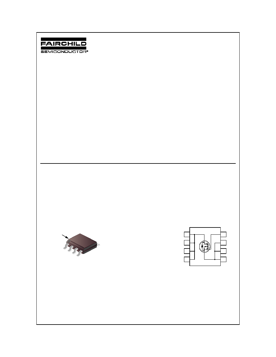
FDS8878
N-Channel PowerTrench
®
MOSFET
30V, 10.2A, 14m
Features
r
DS(ON)
= 14m
, V
GS
= 10V, I
D
= 10.2A
r
DS(ON)
= 17m
, V
GS
= 4.5V, I
D
= 9.3A
High performance trench technology for extremely low
r
DS(ON)
Low gate charge
High power and current handling capability
Applications
DC/DC converters
General Description
This N-Channel MOSFET has been designed specifically to
improve the overall efficiency of DC/DC converters using
either synchronous or conventional switching PWM
controllers. It has been optimized for low gate charge, low
r
DS(ON)
and fast switching speed.
SO-8
Branding Dash
1
5
2
3
4
4
3
2
1
5
6
7
8
FDS887
8 N-Channel
Pow
e
rTr
e
nch
®
MOSFET
FDS8878 Rev. A1
www.fairchildsemi.com
2
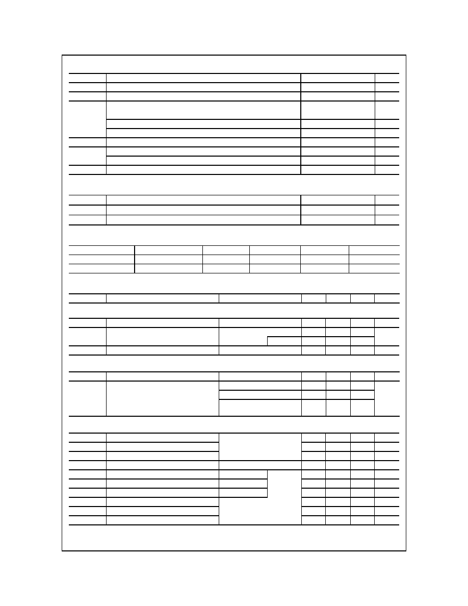
MOSFET Maximum Ratings
T
A
= 25°C unless otherwise noted
Thermal Characteristics
Package Marking and Ordering Information
Electrical Characteristics
T
A
= 25°C unless otherwise noted
Off Characteristics
On Characteristics
Dynamic Characteristics
Symbol
Parameter
Ratings
Units
V
DSS
Drain to Source Voltage
30
V
V
GS
Gate to Source Voltage
±20
V
I
D
Drain Current
10.2
A
Continuous (T
A
= 25
o
C, V
GS
= 10V, R
JA
= 50
o
C/W)
Continuous (T
A
= 25
o
C, V
GS
= 4.5V, R
JA
= 50
o
C/W) 9.3
A
Pulsed
Figure 4
A
E
AS
Single Pulse Avalanche Energy (Note 1)
57
mJ
P
D
Power dissipation
2.5
W
Derate above 25
o
C
20
mW/
o
C
T
J
, T
STG
Operating and Storage Temperature
-55 to 150
o
C
R
JC
Thermal Resistance, Junction to Case (Note 2)
25
o
C/W
R
JA
Thermal Resistance, Junction to Ambient at 10 seconds (Note 3)
50
o
C/W
R
JA
Thermal Resistance, Junction to Ambient at 1000 seconds (Note 3)
85
o
C/W
Device Marking
Device
Package
Reel Size
Tape Width
Quantity
FDS8878
FDS8878
SO-8
330mm
12mm
2500 units
FDS8878
FDS8878_NL (Note 4)
SO-8
330mm
12mm
2500 units
Symbol
Parameter
Test Conditions
Min
Typ
Max
Units
B
VDSS
Drain to Source Breakdown Voltage
I
D
= 250
µA, V
GS
= 0V
30
-
-
V
I
DSS
Zero Gate Voltage Drain Current
V
DS
= 24V
-
-
1
µA
V
GS
= 0V
T
A
= 150
o
C
-
-
250
I
GSS
Gate to Source Leakage Current
V
GS
=
±20V
-
-
±100
nA
V
GS(TH)
Gate to Source Threshold Voltage
V
GS
= V
DS
, I
D
= 250
µA
1.2
-
2.5
V
r
DS(ON)
Drain to Source On Resistance
I
D
= 10.2A, V
GS
= 10V
-
0.0110
0.014
I
D
= 9.3A, V
GS
= 4.5V
-
0.0138
0.017
I
D
= 10.2A, V
GS
= 10V,
T
A
= 150
o
C
-
0.0175
0.0227
C
ISS
Input Capacitance
V
DS
= 15V, V
GS
= 0V,
f = 1MHz
-
897
-
pF
C
OSS
Output Capacitance
-
190
-
pF
C
RSS
Reverse Transfer Capacitance
-
111
-
pF
R
G
Gate Resistance
V
GS
= 0.5V, f = 1MHz
0.7
2.9
5.0
Q
g(TOT)
Total Gate Charge at 10V
V
GS
= 0V to 10V
V
DD
= 15V
I
D
= 10.2A
I
g
= 1.0mA
-
17
26
nC
Q
g(5)
Total Gate Charge at 5V
V
GS
= 0V to 5V
-
9
14
nC
Q
g(TH)
Threshold Gate Charge
V
GS
= 0V to 1V
-
0.9
1.4
nC
Q
gs
Gate to Source Gate Charge
-
2.5
-
nC
Q
gs2
Gate Charge Threshold to Plateau
-
1.7
-
nC
Q
gd
Gate to Drain "Miller" Charge
-
3.3
-
nC
FDS887
8 N-Channel
Pow
e
rTr
e
nch
®
MOSFET
FDS8878 Rev. A1
www.fairchildsemi.com
3
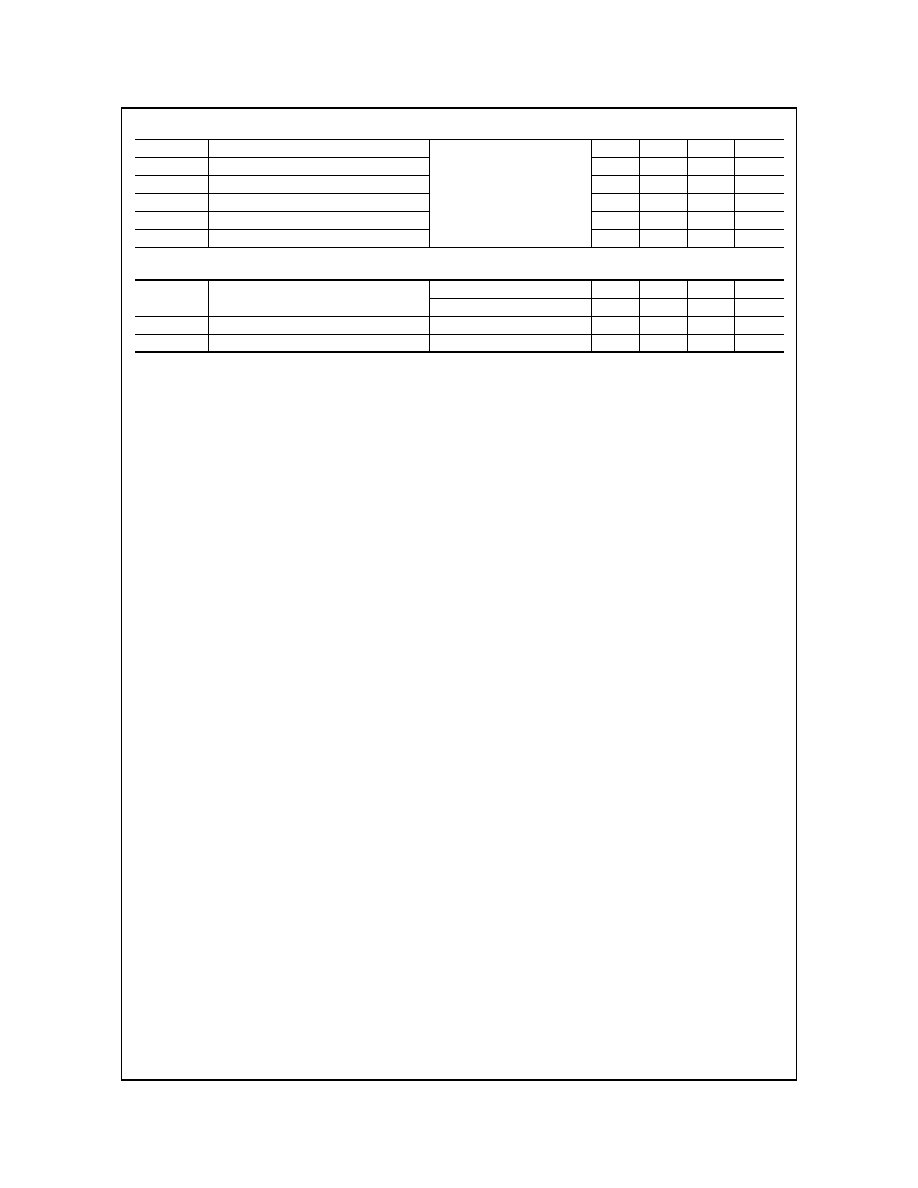
Switching Characteristics
(V
GS
= 10V)
Drain-Source Diode Characteristics
Notes:
1: Starting T
J
= 25°C, L = 1mH, I
AS
= 10.7A, V
DD
= 30V, V
GS
= 10V.
2: R
JA
is the sum of the junction-to-case and case-to-ambient thermal resistance where the case thermal reference is defined as the solder mounting surface of the
drain pins. R
JC
is guaranteed by design while R
JA
is determined by the user's board design.
3: R
JA
is measured with 1.0 in
2
copper on FR-4 board
4: FDS8878_NL is lead free product. FDS8878_NL marking will appear on the reel label.
t
ON
Turn-On Time
V
DD
= 15V, I
D
= 10.2A
V
GS
= 10V, R
GS
= 16
-
-
54
ns
t
d(ON)
Turn-On Delay Time
-
7
-
ns
t
r
Rise Time
-
29
-
ns
t
d(OFF)
Turn-Off Delay Time
-
45
-
ns
t
f
Fall Time
-
18
-
ns
t
OFF
Turn-Off Time
-
-
94
ns
V
SD
Source to Drain Diode Voltage
I
SD
= 10.2A
-
-
1.25
V
I
SD
= 2.1A
-
-
1.0
V
t
rr
Reverse Recovery Time
I
SD
= 10.2A, dI
SD
/dt=100A/
µs
-
-
19
ns
Q
RR
Reverse Recovered Charge
I
SD
= 10.2A, dI
SD
/dt=100A/
µs
-
-
9.5
nC
FDS887
8 N-Channel
Pow
e
rTr
e
nch
®
MOSFET
FDS8878 Rev. A1
www.fairchildsemi.com
4
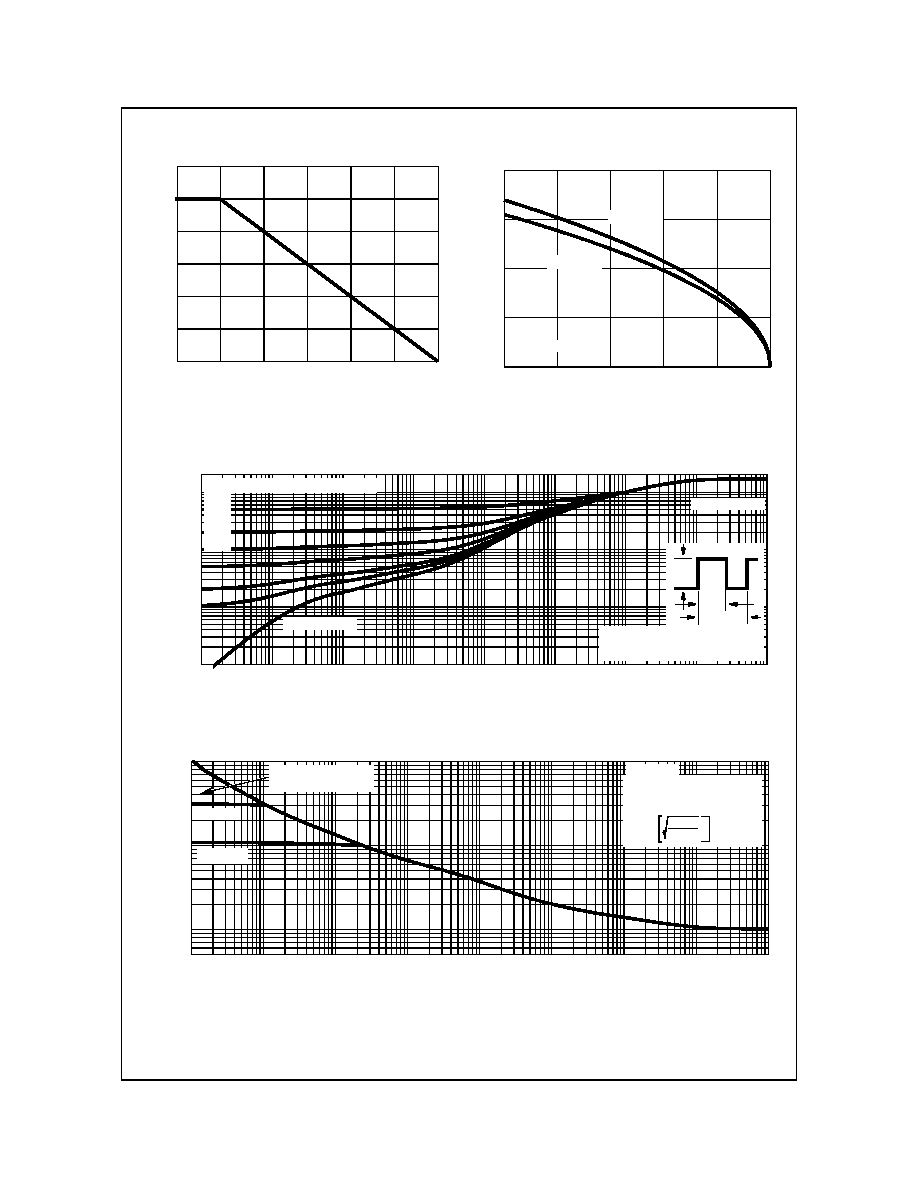
Typical Characteristics
T
A
= 25°C unless otherwise noted
Figure 1. Normalized Power Dissipation vs
Ambient Temperature
Figure 2. Maximum Continuous Drain Current vs
Ambient Temperature
Figure 3. Normalized Maximum Transient Thermal Impedance
Figure 4. Peak Current Capability
T
A
, AMBIENT TEMPERATURE (
o
C)
P
O
W
E
R DIS
S
IP
A
T
ION MUL
T
IP
L
I
E
R
0
0
25
50
75
100
150
0.2
0.4
0.6
0.8
1.0
1.2
125
I
D
,
D
RAIN CURRENT
(
A
)
T
A
, AMBIENT TEMPERATURE (
o
C)
R
JA
=50
o
C/W
V
GS
= 10V
V
GS
= 4.5V
0
3
6
9
12
25
50
75
100
125
150
0.001
0.01
0.1
1
10
-5
10
-4
10
-3
10
-2
10
-1
10
0
10
1
10
2
10
3
2
t, RECTANGULAR PULSE DURATION (s)
Z
JA
, NORM
AL
IZ
ED
SINGLE PULSE
NOTES:
DUTY FACTOR: D = t
1
/t
2
PEAK T
J
= P
DM
x Z
JA
x R
JA
+ T
A
P
DM
t
1
t
2
DUTY CYCLE - DESCENDING ORDER
0.5
0.2
0.1
0.05
0.01
0.02
T
H
ERM
A
L
IM
PE
D
ANCE
R
JA
=50
o
C/W
10
100
1000
5
10
-5
10
-4
10
-3
10
-2
10
-1
10
0
10
1
10
2
10
3
I
DM
, PEAK CU
RRENT
(
A
)
t, PULSE WIDTH (s)
TRANSCONDUCTANCE
MAY LIMIT CURRENT
IN THIS REGION
V
GS
= 10V
T
A
= 25
o
C
I = I
25
150 - T
A
125
FOR TEMPERATURES
ABOVE 25
o
C DERATE PEAK
CURRENT AS FOLLOWS:
V
GS
= 4.5V
FDS887
8 N-Channel
Pow
e
rTr
e
nch
®
MOSFET
FDS8878 Rev. A1
www.fairchildsemi.com
5
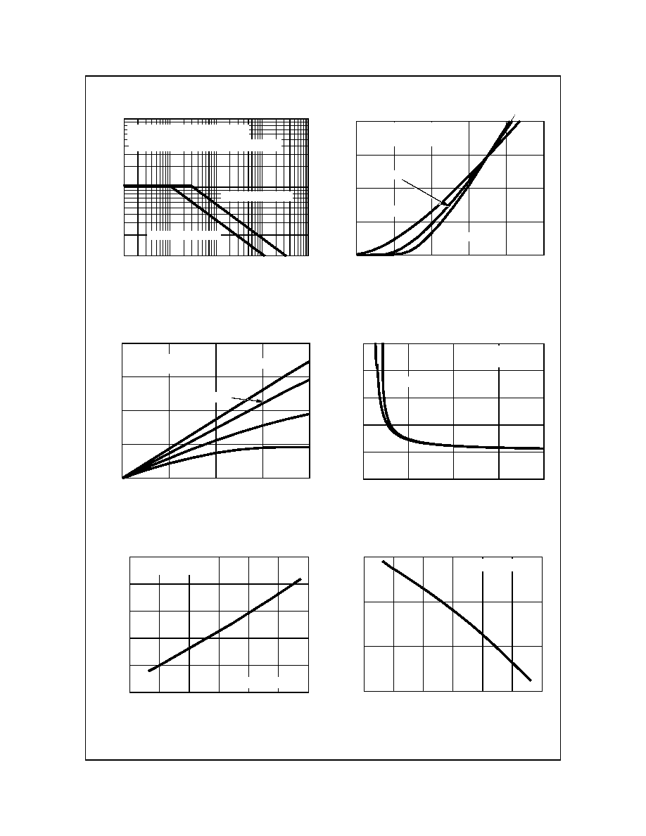
NOTE: Refer to Fairchild Application Notes AN7514 and AN7515
Figure 5. Unclamped Inductive Switching
Capability
Figure 6. Transfer Characteristics
Figure 7. Saturation Characteristics
Figure 8. Drain to Source On Resistance vs Gate
Voltage and Drain Current
Figure 9. Normalized Drain to Source On
Resistance vs Junction Temperature
Figure 10. Normalized Gate Threshold Voltage vs
Junction Temperature
Typical Characteristics
T
A
= 25°C unless otherwise noted
1
10
100
0.01
0.1
1
10
100
I
AS
, A
V
AL
ANCHE
CU
RRENT
(
A
)
t
AV
, TIME IN AVALANCHE (ms)
STARTING T
J
= 25
o
C
STARTING T
J
= 150
o
C
t
AV
= (L)(I
AS
)/(1.3*RATED BV
DSS
- V
DD
)
If R = 0
If R
0
t
AV
= (L/R)ln[(I
AS
*R)/(1.3*RATED BV
DSS
- V
DD
) +1]
I
D
, DRAIN CURREN
T
(
A
)
V
GS
, GATE TO SOURCE VOLTAGE (V)
PULSE DURATION = 80
µs
DUTY CYCLE = 0.5% MAX
V
DD
= 15V
T
J
= 175
o
C
T
J
= 25
o
C
T
J
= -55
o
C
0
20
40
60
80
2.0
2.5
3.0
3.5
4.0
4.5
I
D
,
DRA
I
N
C
URRENT
(
A
)
V
DS
, DRAIN TO SOURCE VOLTAGE (V)
PULSE DURATION = 80
µs
DUTY CYCLE = 0.5% MAX
V
GS
= 3V
V
GS
= 10V
T
A
= 25
o
C
V
GS
= 3.5V
V
GS
= 5V
0
20
40
60
80
0
0.2
0.4
0.6
0.8
0
10
20
30
40
50
2
4
6
8
10
V
GS
, GATE TO SOURCE VOLTAGE (V)
I
D
= 10.2A
r
DS
(
O
N
)
,
DRA
I
N
T
O
SOURCE
ON RE
SIST
ANCE
(
m
)
PULSE DURATION = 80
µs
DUTY CYCLE = 0.5% MAX
I
D
= 1A
0.8
1.0
1.2
1.4
1.6
NORM
AL
IZ
E
D
DRAIN T
O
SOURCE
T
J
, JUNCTION TEMPERATURE (
o
C)
ON RESIS
T
ANCE
V
GS
= 10V, I
D
= 10.2A
PULSE DURATION = 80
µs
DUTY CYCLE = 0.5% MAX
-80
-40
0
40
80
120
160
NORM
AL
IZ
ED GA
T
E
T
J
, JUNCTION TEMPERATURE (
o
C)
V
GS
= V
DS
, I
D
= 250
µA
T
HRE
SHOL
D V
O
L
T
A
GE
0.6
0.8
1.0
1.2
-80
-40
0
40
80
120
160